Table of Contents
Advertisement
Quick Links
Advertisement
Table of Contents

Subscribe to Our Youtube Channel
Related Manuals for Alinx AX7050


Summary of Contents for Alinx AX7050
- Page 1 Spartan-7 FPGA Development Board AX7050 User Manual...
-
Page 2: Version Record
Spartan-7 FPGA Development Board AX7050 User Manual Version Record Version Date Release By Description Rev 1.0 2019-04-25 Rachel Zhou First Release Amazon Store: https://www.amazon.com/alinx 2 / 52... -
Page 3: Table Of Contents
Spartan-7 FPGA Development Board AX7050 User Manual Table of Contents Version Record ..................2 Part 1: FPGA Development Board Introduction ......... 6 Part 2: AC7050 core board ..............10 Part 2.1: AC7050 Core Board Introduction ........10 Part 2.2: FPGA Chip ................12 Part 2.3: Active Differential Crystal ............ - Page 4 Spartan-7 FPGA Development Board AX7050 User Manual Part 3.13: LED Light ................49 Part 3.14: Power Supply ..............50 Part 3.15: Structure Diagram ............. 52 Amazon Store: https://www.amazon.com/alinx 4 / 52...
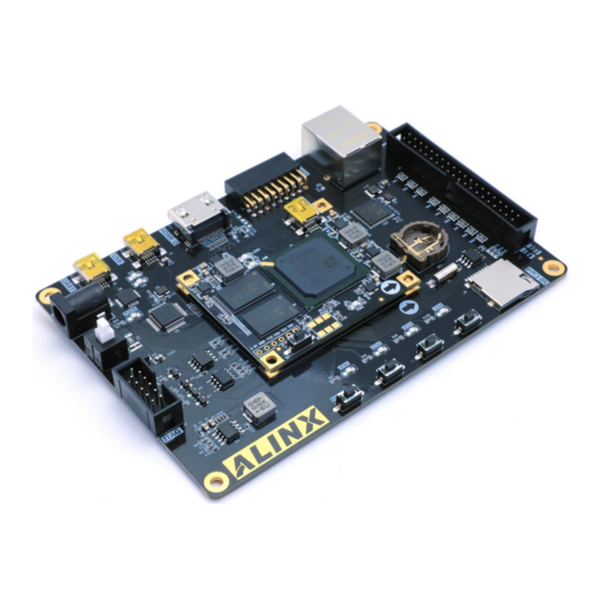
- Page 5 Spartan-7 FPGA Development Board AX7050 User Manual This Spartan7 FPGA development platform adopts the core board + Carrier Board mode, which is convenient for users to use the core board for secondary development. In the design of Carrier Board, we have extended a wealth of interfaces for users, such as Gigabit Ethernet interfaces, HDMI Output interface, USB2.0...
-
Page 6: Part 1: Fpga Development Board Introduction
Spartan-7 FPGA Development Board AX7050 User Manual Part 1: FPGA Development Board Introduction The entire structure of the AX7050 FPGA development board is inherited from our consistent core board + Carrier Board model. A high-speed inter-board connector is used between the core board and the Carrier Board. - Page 7 核心板 SD Card 按键*4 LED*4 Figure 1-1-1: The Schematic Diagram of the AX7050 Through this diagram, you can see the interfaces and functions that the AX7050 FPGA Development Board contains: AC7050 FPGA core board The core board consists of XC7S50 + 2 pieces of 4Gb DDR3 + 128Mb QSPI FLASH.
- Page 8 Spartan-7 FPGA Development Board AX7050 User Manual rate. Full duplex and adaptive 1-channel HDMI Output Use the FPGA's four LVDS differential signals (3-way data plus 1 clock) interface to directly drive the HDMI output, providing different formats of video output interfaces for the FPGA development board ...
- Page 9 Spartan-7 FPGA Development Board AX7050 User Manual JTAG Interface The 10-pin 0.1 spacing standard JTAG ports for FPGA program download and debugging. Button 4 buttons; 1 reset button (on the core board) LED Light 5 user LEDs (1 on the core board and 4 on the Carrier Board) Amazon Store: https://www.amazon.com/alinx...
-
Page 10: Part 2: Ac7050 Core Board
Spartan-7 FPGA Development Board AX7050 User Manual Part 2: AC7050 core board Part 2.1: AC7050 Core Board Introduction AC7050 (core board model, the same below) FPGA core board, it is based on XILINX's Spartan 7 series XC7S50FGGA484. It is a high-performance core board with high speed, high bandwidth and high capacity. - Page 11 Spartan-7 FPGA Development Board AX7050 User Manual Figure 2-1-1: AC7050 Core Board (Front View) Figure 2-1-2: AC7050 Core Board (Rear View) Amazon Store: https://www.amazon.com/alinx 11 / 52...
-
Page 12: Part 2.2: Fpga Chip
Spartan-7 FPGA Development Board AX7050 User Manual Part 2.2: FPGA Chip As mentioned above, the FPGA model we use is XC7S50FGGA484, which belongs to Xilinx's Spartan7 series. The speed grade is 1, and the temperature grade is commercial grade. This model is a FGGA484 package with 484 pins. -
Page 13: Part 2.3: Active Differential Crystal
Spartan-7 FPGA Development Board AX7050 User Manual The main parameters of the FPGA chip XC7S50 are as follows FPGA power supply system XILINX Spartan7 FPGA power supplies are V CCINT CCBRAM CCAUX CCIO is the FPGA core power supply pin, which needs to be connected to 1.0V;... - Page 14 Spartan-7 FPGA Development Board AX7050 User Manual Figure 2-3-1: 50Mhz Active Crystal Oscillator Figure 2-3-2: 50Mhz Active Crystal Oscillator on the Core Board Clock Pin Assignment Signal Name FPGA PIN CLK_50MHZ In addition, an active differential crystal is reserved on the AC7050 core board.
-
Page 15: Part 2.4: Ddr3 Dram
Spartan-7 FPGA Development Board AX7050 User Manual Reserved Differential Clock Pin Assignment Signal Name FPGA PIN SYS_CLK_P SYS_CLK_N Part 2.4: DDR3 DRAM The FPGA core board AC7050 is equipped with two Micron 4Gbit (512MB) DDR3 chips, model MT41J256M16HA-125 (compatible with MT41K256M16HA-125). - Page 16 Spartan-7 FPGA Development Board AX7050 User Manual Data[31:16] DDR3 (MT41J256M16 FPGA BANK 34/35 Addr/control DDR3 Data[15:0] (MT41J256M16 Figure 2-4-1: The DDR3 DRAM Schematic Figure 2-4-2: The DDR3 on the Core Board Amazon Store: https://www.amazon.com/alinx 16 / 52...
- Page 17 Spartan-7 FPGA Development Board AX7050 User Manual DDR3 DRAM pin assignment: Net Name FPGA PIN Name FPGA P/N IO_L2N_T0_AD12N_35 DDR3_DQS0_P IO_L3P_T0_DQS_AD5P_35 DDR3_DQS0_N IO_L9P_T1_DQS_AD7P_35 DDR3_DQS1_P IO_L9N_T1_DQS_AD7N_35 DDR3_DQS1_N IO_L15P_T2_DQS_35 DDR3_DQS2_P IO_L15N_T2_DQS_35 DDR3_DQS2_N IO_L21P_T3_DQS_35 DDR3_DQS3_P IO_L21N_T3_DQS_35 DDR3_DQS3_N IO_L1N_T0_AD4N_35 DDR3_DQ[0] IO_L4N_T0_35 DDR3_DQ [1] IO_L2N_T0_AD12N_35...
- Page 18 Spartan-7 FPGA Development Board AX7050 User Manual IO_L23N_T3_35 DDR3_DQ [25] IO_L22P_T3_35 DDR3_DQ [26] IO_L20P_T3_35 DDR3_DQ [27] IO_L23P_T3_35 DDR3_DQ [28] IO_L22N_T3_35 DDR3_DQ [29] IO_L19P_T3_35 DDR3_DQ [30] IO_L24P_T3_35 DDR3_DQ [31] IO_L4P_T0_35 DDR3_DM0 IO_L8P_T1_AD14P_35 DDR3_DM1 IO_L13P_T2_MRCC_35 DDR3_DM2 IO_L20N_T3_35 DDR3_DM3 IO_L10N_T1_34 DDR3_A[0] IO_L11N_T1_SRCC_34 DDR3_A[1]...
-
Page 19: Part 2.5: Qspi Flash
Spartan-7 FPGA Development Board AX7050 User Manual IO_L12N_T1_MRCC_34 DDR3_CLK_N IO_L3N_T0_DQS_34 DDR3_CKE Part 2.5: QSPI Flash The FPGA core board AC7050 is equipped with one 128MBit QSPI FLASH, and the model is N25Q128, which uses the 3.3V CMOS voltage standard. Due to the non-volatile nature of QSPI FLASH, it can be used as a boot device for the system to store the boot image of the system. -
Page 20: Part 2.6: Led Light On Core Board
Spartan-7 FPGA Development Board AX7050 User Manual QSPI Flash pin assignments: Net Name FPGA PIN Name FPGA P/N CCLK_0 QSPI_CLK IO_L6P_T0_FCS_B_14 QSPI_CS IO_L1P_T0_D00_MOSI_14 QSPI_DQ0 IO_L1N_T0_D01_DIN_14 QSPI_DQ1 IO_L2P_T0_D02_14 QSPI_DQ2 IO_L2N_T0_D03_14 QSPI_DQ3 Figure 2-5-1: QSPI on the Core Board Part 2.6: LED Light on Core Board... -
Page 21: Part 2.7: Jtag Interface
Spartan-7 FPGA Development Board AX7050 User Manual 3.3V 3.3V 3.3V LED1 DONE FPGA DONE Figure 2-6-1: LED lights on core board Schematic Figure 2-6-2: LED lights on the Core Board User LEDs Pin Assignment Signal Name FPGA Pin Number Description... -
Page 22: Part 2.8: Power Interface On The Core Board
Spartan-7 FPGA Development Board AX7050 User Manual the schematic part of the JTAG port, which involves TMS, TDI, TDO, TCK. , GND, +3.3V these six signals. Figure 2-7-1: JTAG Interface Schematic The JTAG interface J1 on AC7050 FPGA core board uses a 6-pin 2.54mm pitch single-row test hole. -
Page 23: Part 2.9: Board To Board Connectors Pin Assignment
Spartan-7 FPGA Development Board AX7050 User Manual Figure 2-8-1:MINI USB interface schematic Figure 2-8-2:MINI USB interface on the Core Board Part 2.9: Board to Board Connectors pin assignment The core board has a total of two high-speed board to board connectors. - Page 24 Spartan-7 FPGA Development Board AX7050 User Manual Board to Board Connectors CON1 The 80-pin board to board connectors CON1, which is used to connect the normal IO of FPGA (which contains 6 pairs of differential interface IO, can be used as LVDS data communication), the default IO level is 3.3V. The pin assignment of the CON1 expansion port is shown in Table 2-9-1.
- Page 25 Spartan-7 FPGA Development Board AX7050 User Manual PIN53 B16_L18_N PIN54 B16_L11_P PIN55 B16_L18_P PIN56 B16_L11_N PIN57 Ground PIN58 B16_L12_P PIN59 B16_L14_N PIN60 B16_L12_N PIN61 B16_L14_P PIN62 B16_L5_N PIN63 Ground PIN64 Ground PIN65 B16_L9_N PIN66 B16_L5_P PIN67 B16_L9_P PIN68 B16_L3_N PIN69...
- Page 26 Spartan-7 FPGA Development Board AX7050 User Manual Pin Assignment of Board to Board Connectors CON2 CON2 FPGA Input/ CON2 FPGA Input/ Name Output Name Output PIN1 Power PIN2 Power PIN3 Power PIN4 Power PIN5 Power PIN6 Power PIN7 Power PIN8...
-
Page 27: Part 2.10: Power Supply
Spartan-7 FPGA Development Board AX7050 User Manual PIN67 B14_L18_N PIN68 B15_L6_P PIN69 B14_L18_P PIN70 Ground PIN71 B14_L17_N N.C. PIN72 B15_L4_N PIN73 B14_L17_P N.C. PIN74 B15_L4_P PIN75 Ground PIN76 Ground PIN77 PIN78 PIN79 PIN80 The pins of B15_L14_P/N, B15_L16_P/N, B15_L5_P/N, B15_L13_P/N, B15_L6_P/N and B15_L4_P/N are differentially derived on the PCB and can be used as high-speed LVDS data communication. - Page 28 Spartan-7 FPGA Development Board AX7050 User Manual 1.0V/3A TPS54620 Mini USB TLV62130R 1.8V/3A CON2 TLV62130R 1.5V/3A TPS51200 VREF 3.3V/0.5A SPX3819M5 -3-3 SPX3819M5 VCCIO/0.5A -3-3 Figure 2-10-1:Power Supply on core board schematic The core board is powered by +5V, converted to +1.0V by a 1 channel DC/DC power chip TPS54620, and the output current can be as high as 6A.
- Page 29 Spartan-7 FPGA Development Board AX7050 User Manual +1.8V FPGA auxiliary voltage +3.3V VCCIO of Bank0 and Bank14 of FPGA,QSIP FLASH, Clock Crystal +1.5V DDR3, Bank34 and Bank35 of FPGA VREF,VTT(+0.75V) DDR3 VCCIO(+3.3V) FPGA Bank15, Bank16 The power circuit on the AC7050 FPGA core board is shown in Figure...
-
Page 30: Part 2.12: Structure Diagram
Spartan-7 FPGA Development Board AX7050 User Manual Figure 2-11-3: Power Supply on the AC7050 FPGA Core Board (Bottom View) Part 2.12: Structure Diagram Figure 2-12-1: AC7050 FPGA Core board (Top view) Amazon Store: https://www.amazon.com/alinx 30 / 52... - Page 31 Spartan-7 FPGA Development Board AX7050 User Manual Figure 2-12-2: AC7050 FPGA Core board (Bottom view) Amazon Store: https://www.amazon.com/alinx 31 / 52...
-
Page 32: Part 3: Carrier Board
Spartan-7 FPGA Development Board AX7050 User Manual Part 3: Carrier Board Part 3.1: Carrier Board Introduction Through the previous function introduction, you can understand the function of the Carrier Board part 1-channel 10/100M/1000M Ethernet RJ-45 interface 1-channel HDMI video output interface ... -
Page 33: Part 3.2: Gigabit Ethernet Interface
4 independent buttons 4 user LED lights Part 3.2: Gigabit Ethernet Interface The AX7050 FPGA development board provides users with one-channel Gigabit network communication service through the Realtek RTL8211EG Ethernet PHY chip. The RTL8211EG chip supports 10/100/1000 Mbps network transmission rate and data communicates with the FPGA through the RGMII interface. - Page 34 Spartan-7 FPGA Development Board AX7050 User Manual transmission clock is 25Mhz. Both the receive clock E_RXC and the transmit clock E_TXC are provided by the PHY chip, and data is sampled on the rising edge of the clock.. RTL8211EG E_TXD[3:0]...
-
Page 35: Part 3.3: Hdmi Output Interface
Spartan-7 FPGA Development Board AX7050 User Manual E_TXD1 Transmit Data bit1 E_TXD2 Transmit Data bit2 E_TXD3 Transmit Data bit3 E_TXEN Transmit enable signal E_TXC 100M/10 Send Clock E_RXC RGMII Receive clock E_RXD0 Receive Data Bit0 E_RXD1 Receive Data Bit1 E_RXD2... - Page 36 Spartan-7 FPGA Development Board AX7050 User Manual HDMI_CLK_P/N HDMI_D2_P/N FPGA HDMI_D1_P/N HDMI_D0_P/N Spartan7 TVS管 Figure 3-3-1: HDMI Output Interface Schematic Figure 3-3-2: HDMI Output Interface on the Carrier Board HDMI Pin Assignment Net Name FPGA PIN HDMI_CLK_P HDMI_CLK_N HDMI_D2_N HDMI_D2_P HDMI_D1_N Amazon Store: https://www.amazon.com/alinx...
-
Page 37: Part 3.4: Usb2.0 Interface
Spartan-7 FPGA Development Board AX7050 User Manual HDMI_D1_P HDMI_D0_N HDMI_D0_P Part 3.4: USB2.0 Interface We used FTDI Chip's FT232H single-channel high-speed USB chip to realize USB2.0 data communication between the FPGA development board and the computer. Maximum USB2.0 high-speed communication (480Mb/s) and full-speed communication (12Mb/s). - Page 38 Spartan-7 FPGA Development Board AX7050 User Manual Figure 3-4-2: USB 2.0 part on the Carrier Board USB 2.0 Pin Assignment Signal Name FPGA PIN Description USB_FD0 USB2.0 data Bit0 USB_FD1 USB2.0 data Bit1 USB_FD2 USB2.0 data Bit2 USB_FD3 USB2.0 data Bit3 USB_FD4 USB2.0 data Bit4...
-
Page 39: Part 3.5: Sd Card Slot
Spartan-7 FPGA Development Board AX7050 User Manual Part 3.5: SD Card Slot The SD card (Secure Digital Memory Card) is a memory card based on the semiconductor flash memory process. It was completed in 1999 by the Japanese Panasonic-led concept, and the participants Toshiba and SanDisk of the United States conducted substantial research and development. -
Page 40: Part 3.6: Usb To Serial Port
SD_DATA_OUT Part 3.6: USB to Serial Port The AX7050 FPGA development board includes the USB-UAR chip of Silicon Labs CP2102GM. The USB interface uses the MINI USB interface, which can be connected to the USB port of the upper PC for serial data communication with a USB cable. - Page 41 Spartan-7 FPGA Development Board AX7050 User Manual Micro USB UART_TXD FPGA VBUS REGIN Spartan7 CP2102 UART_RXD D+/- Figure 3-6-1: USB to serial port schematic Figure 3-6-2: USB to serial port on the Carrier Board At the same time, two LED indicators are set for the serial port signal, and...
-
Page 42: Part 3.7: Eeprom 24Lc04
UART1_TXD Part 3.7: EEPROM 24LC04 AX7050 FPGA Carrier Board contains an EEPROM, model 24LC04, and has a capacity of 4Kbit (2*256*8bit). It consists of two 256-byte blocks and communicates via the IIC bus. The onboard EEPROM is to learn how to communicate with the IIC bus. -
Page 43: Part 3.8 : Real Time Clock Ds1302
I2C_SDA Part 3.8 : Real time clock DS1302 The AX7050 FPGA Carrier Board contains a real-time clock RTC chip, model DS1302, which provides a calendar function up to 2099, with days, minutes, minutes, seconds and weeks. If time is needed in the system, then the RTC needs to be involved in the product. -
Page 44: Part 3.9: Expansion Header
Part 3.9: Expansion Header The AX7050 FPGA Carrier Board is reserved with one 2.54-mm standard 40-pin expansion ports J8, which is used to connect the ALINX modules or the external circuit designed by the user. The expansion port has 40 signals, of which 1-channel 5V power supply, 2-channel 3.3 V power supply, 3-channle... - Page 45 Spartan-7 FPGA Development Board AX7050 User Manual Figure 3-9-1: Expansion header J8 schematic Figure 3-9-2: Expansion header J8 on the Carrier Board J8 Expansion Header Pin Assignment Pin Number FPGA Pin Pin Number FPGA Pin Amazon Store: https://www.amazon.com/alinx 45 / 52...
-
Page 46: Part 3.10: Jtag Interface
+3.3V Part 3.10: JTAG Interface A standard 10-pin 2.54mm pitch JTAG interface is reserved on the AX7050 FPGA Carrier Board for downloading FPGA programs or firmware to FLASH. In order to prevent damage to the FPGA chip caused by hot plugging, a protection diode is added to the JTAG signal to ensure that the voltage of the signal is within the range accepted by the FPGA to avoid damage of the FPGA chip. -
Page 47: Part 3.11: Camera Module Interface
Be careful not to hot swap when JTAG cable is plugged and unplugged. Part 3.11: Camera Module Interface The AX7050 FPGA Carrier Board includes an 18-pin CMOS camera interface for connecting ALINX's OV5640 camera module for video capture. After acquisition, the monitor can be connected via HDMI or VGA. Regarding the camera selection, the user can purchase as needed. -
Page 48: Part 3.12: Buttons
CMOS_PWDN Part 3.12: Buttons The AX7050 FPGA Carrier Board contains four user buttons KEY1~KEY4. All buttons are connected to the normal IO of the FPGA. The button is active low. When the button is pressed, the IO input voltage of the FPGA is low. When Amazon Store: https://www.amazon.com/alinx... - Page 49 KEY4 Part 3.13: LED Light There are seven red LEDs on the AX7050 FPGA Carrier Board, one of which is the power indicator (PWR), two are USB Uart data receiving and transmitting indicators, and four are users LED lights (LED1~LED4). When the board is powered on, the power indicator will light up;...
- Page 50 LED4 Part 3.14: Power Supply The power input voltage of the AX7050 FPGA development board is DC5V. The Carrier Board converts the +5V voltage to a +3.3V power supply via a 1-way DC/DC power supply chip MP1482. In addition, the +5V power supply on the Carrier Board supplies power to the core board through the inter-board Amazon Store: https://www.amazon.com/alinx...
- Page 51 Spartan-7 FPGA Development Board AX7050 User Manual connector. The +3.3V power supply design on the expansion is shown in Figure 3-14-1. Figure 3-14-1: Power Design Schematic on the Carrier Board Figure 3-14-2: +3.3V Power circuit on the Carrier Board Amazon Store: https://www.amazon.com/alinx...
- Page 52 Spartan-7 FPGA Development Board AX7050 User Manual Part 3.15: Structure Diagram Figure 3-15-1: Structure Diagram of Carrier Board (Top View) Amazon Store: https://www.amazon.com/alinx 52 / 52...
Need help?
Do you have a question about the AX7050 and is the answer not in the manual?
Questions and answers