Table of Contents
Advertisement
Quick Links
Advertisement
Table of Contents

Related Manuals for Alinx ARTIX-7FPGA


Summary of Contents for Alinx ARTIX-7FPGA
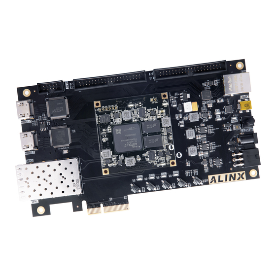
- Page 1 ARTIX-7 FPGA Development Board AX7201 User Manual...
-
Page 2: Version Record
ARTIX-7 FPGA Development Board AX7201 User Manual Version Record Version Date Release By Description Rev 1.2 2023-02-23 Rachel Zhou First Release 2 / 53 www.alinx.com... -
Page 3: Table Of Contents
Part 3.4: VGA display interface ............43 Part 3.5: USB to Serial Port ..............46 Part 3.6: Expansion Header ............... 48 Part 3.7: JTAG Interface ..............49 Part 3.8: Keys ..................50 Part 3.9: LED Light ................51 Part 3.10: Power Supply ..............52 3 / 53 www.alinx.com... - Page 4 ARTIX-7 FPGA Development Board AX7201 User Manual 4 / 53 www.alinx.com...
- Page 5 FPGA development platform. It provides the applications for multi-channel video transmission, multi-channel networks, fiber-optic communication, and data processing. This product is very suitable for students, engineers and other groups engaged data communication and video image processing. 5 / 53 www.alinx.com...
-
Page 6: Part 1: Fpga Development Board Introduction
800Mhz, which fully meets the needs of high-speed multi-channel data processing. In addition, the XC7A200T FPGA features four GTP high-speed transceivers with speeds up to 6.6Gb/s per channel, making it ideal for fiber-optic communications and PCIe data communications. 6 / 53 www.alinx.com... - Page 7 4-channel Gigabit Ethernet Interface RJ-45 interface The Gigabit Ethernet interface chip uses Realtek's RTL8211EG Ethernet PHY chip to provide network communication services to users. RTL8211EG chip supports 10/100/1000 Mbps network transmission rate. Full duplex and adaptive 7 / 53 www.alinx.com...
- Page 8 40-pin expansion port 40-pin 0.1inch spacing expansion port can be connected to various ALINX modules (binocular camera, TFT LCD screen, high-speed AD module, etc.). The expansion port contains 1 channel 5V power supply, 2 channel 3.3V power supply, 3 way ground, 34 IOs port.
-
Page 9: Part 2: Ac7200 Core Board Introduction
For users who need a lot of IO, this core board will be a good choice. Moreover, the routing between the FPGA chip and the interface is equal length and differential processing, and the core board size is only 45*55 (mm), which is very suitable for secondary development. 9 / 53 www.alinx.com... -
Page 10: Part 2.1: Fpga Chip
Xilinx's Artix-7 series. The speed grade is 2, and the temperature grade is industry grade. This model is a FGG484 package with 484 pins. Xilinx ARTIX-7 FPGA chip naming rules as below The Specific Chip Model Definition of ARTIX-7 Series 10 / www.alinx.com... - Page 11 FPGA core power supply pin, which needs to be connected MGTAVTT CCINT to 1.0V; V is the power supply pin of FPGA block RAM, connect to 1.0V; CCBRAM is FPGA auxiliary power supply pin, connect 1.8V; V is the voltage of CCAUX 11 / www.alinx.com...
-
Page 12: Part 2.2: Active Differential Crystal
BANK34 global clock pin MRCC (R4 and T4) of the FPGA. This 200Mhz differential clock can be used to drive the user logic in the FPGA. Users can configure the PLLs and DCMs inside the FPGA to generate clocks of different frequencies. 12 / www.alinx.com... -
Page 13: Part 2.4: 148.5Mhz Active Differential Crystal
G2 is the 148.5Mhz active differential crystal, which is the reference input clock provided to the GTP module inside the FPGA. The crystal output is connected to the GTP BANK216 clock pins MGTREFCLK0P (F6) and MGTREFCLK0N (E6) of the FPGA. 13 / www.alinx.com... - Page 14 ARTIX-7 FPGA Development Board AX7201 User Manual 148.5Mhz Active Differential Crystal Schematic 1148.5Mhz Active Differential Crystal on the Core Board 125Mhz Differential Clock Pin Assignment Net Name FPGA PIN MGT_CLK0_P MGT_CLK0_N 14 / www.alinx.com...
-
Page 15: Part 2.5: Ddr3 Dram
The hardware design of DDR3 requires strict consideration of signal integrity. We have fully considered the matching resistor/terminal resistance, trace impedance control, and trace length control in circuit design and PCB design to ensure high-speed and stable operation of DDR3. The DDR3 DRAM Schematic 15 / www.alinx.com... - Page 16 FPGA PIN Name FPGA P/N DDR3_DQS0_P IO_L3P_T0_DQS_AD5P_35 DDR3_DQS0_N IO_L3N_T0_DQS_AD5N_35 DDR3_DQS1_P IO_L9P_T1_DQS_AD7P_35 DDR3_DQS1_N IO_L9N_T1_DQS_AD7N_35 DDR3_DQS2_P IO_L15P_T2_DQS_35 DDR3_DQS2_N IO_L15N_T2_DQS_35 DDR3_DQS3_P IO_L21P_T3_DQS_35 DDR3_DQS3_N IO_L21N_T3_DQS_35 DDR3_DQ[0] IO_L2P_T0_AD12P_35 DDR3_DQ [1] IO_L5P_T0_AD13P_35 DDR3_DQ [2] IO_L1N_T0_AD4N_35 DDR3_DQ [3] IO_L6P_T0_35 DDR3_DQ [4] IO_L2N_T0_AD12N_35 DDR3_DQ [5] IO_L5N_T0_AD13N_35 16 / www.alinx.com...
- Page 17 DDR3_DQ [26] IO_L20P_T3_35 DDR3_DQ [27] IO_L22N_T3_35 DDR3_DQ [28] IO_L23P_T3_35 DDR3_DQ [29] IO_L24N_T3_35 DDR3_DQ [30] IO_L24P_T3_35 DDR3_DQ [31] IO_L22P_T3_35 DDR3_DM0 IO_L4N_T0_35 DDR3_DM1 IO_L8N_T1_AD14N_35 DDR3_DM2 IO_L16N_T2_35 DDR3_DM3 IO_L23N_T3_35 DDR3_A[0] IO_L11N_T1_SRCC_34 DDR3_A[1] IO_L8N_T1_34 DDR3_A[2] IO_L10P_T1_34 DDR3_A[3] IO_L10N_T1_34 DDR3_A[4] IO_L7N_T1_34 DDR3_A[5] IO_L6P_T0_34 17 / www.alinx.com...
- Page 18 IO_L2N_T0_34 DDR3_A[9] IO_L2P_T0_34 DDR3_A[10] IO_L5N_T0_34 DDR3_A[11] IO_L4P_T0_34 DDR3_A[12] IO_L4N_T0_34 DDR3_A[13] IO_L1N_T0_34 DDR3_A[14] IO_L6N_T0_VREF_34 DDR3_BA[0] IO_L9N_T1_DQS_34 DDR3_BA[1] IO_L9P_T1_DQS_34 DDR3_BA[2] IO_L11P_T1_SRCC_34 DDR3_S0 IO_L8P_T1_34 DDR3_RAS IO_L12P_T1_MRCC_34 DDR3_CAS IO_L12N_T1_MRCC_34 DDR3_WE IO_L7P_T1_34 DDR3_ODT IO_L14N_T2_SRCC_34 DDR3_RESET IO_L15P_T2_DQS_34 DDR3_CLK_P IO_L3P_T0_DQS_34 DDR3_CLK_N IO_L3N_T0_DQS_34 DDR3_CKE IO_L14P_T2_SRCC_34 18 / www.alinx.com...
-
Page 19: Part 2.6: Qspi Flash
FPGA chip. The clock pin is connected to CCLK0 of BANK0, and other data and chip select signals are connected to D00~D03 and FCS pins of BANK14 respectively. Shows the hardware connection of QSPI Flash. QSPI Flash Schematic QSPI Flash pin assignments: 19 / www.alinx.com... - Page 20 ARTIX-7 FPGA Development Board AX7201 User Manual Net Name FPGA PIN Name FPGA P/N QSPI_CLK CCLK_0 QSPI_CS IO_L6P_T0_FCS_B_14 QSPI_DQ0 IO_L1P_T0_D00_MOSI_14 QSPI_DQ1 IO_L1N_T0_D01_DIN_14 QSPI_DQ2 IO_L2P_T0_D02_14 QSPI_DQ3 IO_L2N_T0_D03_14 QSPI on the Core Board 20 / www.alinx.com...
-
Page 21: Part 2.7: Led Light On Core Board
LED will be lit. The schematic diagram of the LED light hardware connection is shown: LED lights on core board Schematic LED lights on the Core Board User LEDs Pin Assignment Signal Name FPGA Pin Name FPGA Pin Number Description LED1 IO_L15N_T2_DQS_34 User LED 21 / www.alinx.com... -
Page 22: Part 2.8: Reset Button
IO is high. The schematic diagram of the reset button connection is shown: Reset Button Schematic Reset button on the Core Board Reset button pin assignment Signal Name ZYNQ Pin Name ZYNQ Pin Number Description RESET_N IO_L17N_T2_34 FPGA system reset 22 / www.alinx.com... -
Page 23: Part 2.9: Jtag Interface
If you need to use the JTAG connection to debug on the core board, you need to solder a 6-pin single-row pin header. shows the JTAG interface J1 on the AC7200 FPGA core board. JTAG Interface on Core Board 23 / www.alinx.com... -
Page 24: Part 2.10: Power Interface On The Core Board
2PIN power interface (J3). When the user supplies power to the core board through 2PIN power interface (J3), it cannot be powered through the carrier board. Otherwise, current conflict may occur. Power Interface on the Core Board 24 / www.alinx.com... -
Page 25: Part 2.11: Board To Board Connectors
Pin Assignment of Board to Board Connectors CON1 CON1 Signal Name FPGA Pin CON1 Signal Name FPGA Pin Voltage Voltage Level Level PIN1 VCCIN PIN2 VCCIN PIN3 VCCIN PIN4 VCCIN PIN5 VCCIN PIN6 VCCIN PIN7 VCCIN PIN8 VCCIN PIN9 Ground PIN10 Ground 25 / www.alinx.com... - Page 26 1.5V PIN55 PIN56 B34_L24_P 1.5V PIN57 PIN58 B34_L24_N 1.5V PIN59 Ground PIN60 Ground PIN61 B16_L1_N 3.3V PIN62 PIN63 B16_L1_P 3.3V PIN64 PIN65 B16_L4_N 3.3V PIN66 PIN67 B16_L4_P 3.3V PIN68 PIN69 Ground PIN70 Ground PIN71 B16_L6_N 3.3V PIN72 26 / www.alinx.com...
- Page 27 PIN36 B14_L7_N 3.3V PIN37 B13_L8_P 3.3V PIN38 B14_L7_P 3.3V PIN39 Ground PIN40 Ground PIN41 B14_L11_N 3.3V PIN42 B14_L4_P 3.3V PIN43 B14_L11_P 3.3V PIN44 B14_L4_N 3.3V PIN45 B14_L14_N 3.3V PIN46 B14_L9_P 3.3V PIN47 B14_L14_P 3.3V PIN48 B14_L9_N 3.3V 27 / www.alinx.com...
- Page 28 CON1 Signal Name FPGA Voltage CON1 Signal Name FPGA Pin Voltage Level Level PIN1 B15_IO0 3.3V PIN2 B15_IO25 3.3V PIN3 B16_IO0 3.3V PIN4 B16_IO25 3.3V PIN5 B15_L4_P 3.3V PIN6 B16_L21_N 3.3V PIN7 B15_L4_N 3.3V PIN8 B16_L21_P 3.3V 28 / www.alinx.com...
- Page 29 Ground PIN60 Ground PIN61 B15_L23_P 3.3V PIN62 B15_L18_P 3.3V PIN63 B15_L23_N 3.3V PIN64 B15_L18_N 3.3V PIN65 B15_L22_P 3.3V PIN66 B15_L17_N 3.3V PIN67 B15_L22_N 3.3V PIN68 B15_L17_P 3.3V PIN69 Ground PIN70 Ground PIN71 B15_L24_P 3.3V PIN72 B15_L16_P 3.3V 29 / www.alinx.com...
- Page 30 MGT_TX3_P Differential PIN18 MGT_RX2_P Differential PIN19 MGT_TX3_N Differential PIN20 MGT_RX2_N Differential PIN21 Ground PIN22 Ground PIN23 MGT_RX3_P Differential PIN24 MGT_TX0_P Differential PIN25 MGT_RX3_N Differential PIN26 MGT_TX0_N Differential PIN27 Ground PIN28 Ground PIN29 MGT_TX1_P Differential PIN30 MGT_RX0_P Differential 30 / www.alinx.com...
- Page 31 3.3V PIN67 B16_L15_N 3.3V PIN68 B16_L16_N 3.3V PIN69 Ground PIN70 Ground PIN71 B16_L17_P 3.3V PIN72 B16_L18_P 3.3V PIN73 B16_L17_N 3.3V PIN74 B16_L18_N 3.3V PIN75 B16_L19_P 3.3V PIN76 B16_L20_P 3.3V PIN77 B16_L19_N 3.3V PIN78 B16_L20_N 3.3V PIN79 PIN80 31 / www.alinx.com...
-
Page 32: Part 2.12: Power Supply
VTT and VREF voltages required by DDR3 via TI's TPS51200. The 1.8V power supply MGTAVTT MGTAVCC for the GTP transceiver is generated by TI's TPS74801 chip. The functions of each power distribution are shown in the following table: 32 / www.alinx.com... -
Page 33: Part 2.13: Structure Diagram
1.0V->1.8V->(1.5 V, 3.3V, VCCIO) and 1.0V-> MGTAVCC -> MGTAVTT, the circuit design to ensure the normal operation of the chip. Part 2.13: Structure Diagram 33 / www.alinx.com... -
Page 34: Part 3: Carrier Board
4-channel 10/100M/1000M Ethernet RJ-45 interface 4-channel SFP interface 1-channel 16-bit VGA output interface 1-channel USB Uart debug interface 40-pin expansion ports JTAG debugging interface 2 independent Keys 2 user LED lights 34 / www.alinx.com... -
Page 35: Part 3.2: Gigabit Ethernet Interface
FPGA and PHY chip RTL8211EG is communicated through the GMII bus, the transmission clock is 25Mhz. The receive clock E_RXC is provided by the PHY chip, the transmit clock E_GTXC is provided by the FPGA, and the data is 35 / www.alinx.com... - Page 36 ARTIX-7 FPGA Development Board AX7201 User Manual sampled on the rising edge of the clock. Figure 3-2-1: Gigabit Ethernet Interface Schematic Figure 3-3-2: Gigabit Ethernet interface on the Carrier Board 36 / www.alinx.com...
- Page 37 Ethernet Receive Data Bit4 E1_RXD5 Ethernet Receive Data Bit5 E1_RXD6 Ethernet Receive Data Bit6 E1_RXD7 Ethernet Receive Data Bit7 E1_COL Ethernet Collision signal E1_CRS Ethernet Carrier Sense Signal E1_RESET Ethernet Reset Signal E1_MDC Ethernet Management Clock E1_MDIO Ethernet Management Data 37 / www.alinx.com...
- Page 38 Ethernet Receive Data Bit5 E2_RXD6 Ethernet Receive Data Bit6 E2_RXD7 Ethernet Receive Data Bit7 E2_COL Ethernet Collision signal E2_CRS Ethernet Carrier Sense Signal E2_RESET Ethernet Reset Signal E2_MDC AB21 Ethernet Management Clock E2_MDIO AB22 Ethernet Management Data 38 / www.alinx.com...
- Page 39 Ethernet Receive Data Bit4 E3_RXD5 Ethernet Receive Data Bit5 E3_RXD6 Ethernet Receive Data Bit6 E3_RXD7 Ethernet Receive Data Bit7 E3_COL Ethernet Collision signal E3_CRS Ethernet Carrier Sense Signal E3_RESET Ethernet Reset Signal E3_MDC Ethernet Management Clock E3_MDIO Ethernet Management Data 39 / www.alinx.com...
- Page 40 Ethernet Receive Data Bit4 E4_RXD5 Ethernet Receive Data Bit5 E4_RXD6 Ethernet Receive Data Bit6 E4_RXD7 Ethernet Receive Data Bit7 E4_COL Ethernet Collision signal E4_CRS Ethernet Carrier Sense Signal E4_RESET Ethernet Reset Signal E4_MDC Ethernet Management Clock E4_MDIO Ethernet Management Data 40 / www.alinx.com...
-
Page 41: Part 3.3: Sfp Interface
The TX and RX data rates are up to each 6.6Gb/s per channel. The reference clock for the GTX transceiver is provided by the 125Mhz differential clock of AC7100B FPGA core board. Figure 3-3-1 detailed the schematic diagram of FPGA and fiber design Figure 3-3-1: SFP Interface Schematic 41 / www.alinx.com... - Page 42 SFP1 Data Transfer (Positive) SFP1_TX_N SFP1 Data Transfer (Negative) SFP1_RX_P SFP1 Data Receiver (Positive) SFP1_RX_P SFP1 Data Receiver (Negative) SFP1_TX_DIS SFP1 Optical Transfer Disable, active high SFP1_LOSS SFP1 Optical LOSS, High level means no light signal is received 42 / www.alinx.com...
-
Page 43: Part 3.4: Vga Display Interface
D-Sub interface. The VGA interface is a D-type interface with a total of 15 pinholes, divided into three rows, five in each row. More important are three RGB color component signals and two scan sync signals HSYNC and 43 / www.alinx.com... - Page 44 The digital to analog signal of the VGA is realized by a simple resistor circuit. This resistor circuit can generate 32 gradient grade red and blue signals and 64 gradient grade green signals (RGB 5-6-5). The VGA interface part of the circuit is shown in Figure 3-4-2. 44 / www.alinx.com...
- Page 45 ARTIX-7 FPGA Development Board AX7201 User Manual Figure 3-4-2: VGA Display Interface Schematic Figure 3-4-3: VGA Display Interface on the Carrier Board VGA Pin Assignment: Signal Name FPGA Pin Description VGA_B[0] BLUE[0] VGA_B[1] BLUE[1] VGA_B[2] BLUE[2] VGA_B[3] BLUE[3] 45 / www.alinx.com...
-
Page 46: Part 3.5: Usb To Serial Port
USB port of the upper PC for serial data communication with a USB cable. The schematic diagram of the USB Uart circuit design is shown in Figure 3-5-1: Figure 3-5-1: USB to serial port schematic 46 / www.alinx.com... - Page 47 PCB is TX and RX, indicating that the serial port has data transmission or reception, as shown in the following Figure 3-5-3 Figure 3-5-3: Serial Port communication LED Indicators Schematic USB to serial port pin assignment: Signal Name FPGA PIN UART_RXD AA15 UART_TXD AB15 47 / www.alinx.com...
-
Page 48: Part 3.6: Expansion Header
Part 3.6: Expansion Header The AX7201 FPGA carrier board is reserved with one 0.1inch spacing standard 40-pin expansion header J11 which is used to connect the ALINX modules or the external circuit designed by the user. The expansion port has 40 signals, of which 1-channel 5V power supply, 2-channel 3.3 V power supply,... -
Page 49: Part 3.7: Jtag Interface
FPGA chip caused by hot plugging, a protection diode is added to the JTAG signal to ensure that the voltage of the signal is within the range accepted by the FPGA to avoid damage of the FPGA chip. 49 / www.alinx.com... -
Page 50: Part 3.8: Keys
Key is pressed, the IO input voltage of the FPGA is low. When no Key is pressed, The IO input voltage of the FPGA is high. The circuit of the Key part is shown in Figure 3-8-1. 50 / www.alinx.com... -
Page 51: Part 3.9: Led Light
LED is configured low level, the user LED lights up. When the connected IO voltage is configured as high level, the user LED will be extinguished. The schematic diagram of the user LEDs hardware connection is shown in Figure 3-9-1. 51 / www.alinx.com... -
Page 52: Part 3.10: Power Supply
DC/DC power chip MP1482. In addition, the +5V power supply on the Carrier Board supplies power to the core board through the inter-board connector. The power supply design on the expansion is shown in Figure 3-10-1. 52 / www.alinx.com... - Page 53 ARTIX-7 FPGA Development Board AX7201 User Manual Figure 3-10-1 Power Design Schematic on the Carrier Board Figure 3-10-2: Power circuit on the Carrier Board 53 / www.alinx.com...
Need help?
Do you have a question about the ARTIX-7FPGA and is the answer not in the manual?
Questions and answers