Table of Contents
Advertisement
Quick Links
Advertisement
Table of Contents

Related Manuals for Alinx AX7035


Summary of Contents for Alinx AX7035
- Page 1 ARTIX-7 FPGA Development Board AX7035 User Manual...
-
Page 2: Version Record
2019-04-26 Rachel Zhou First Release The English version was translated by Shanghai Tianhui Trading Company. They has not been officially Review by ALINX and are for reference only. If there are any errors, please send email to rachel.zhou@aithtech.com for correction. -
Page 3: Table Of Contents
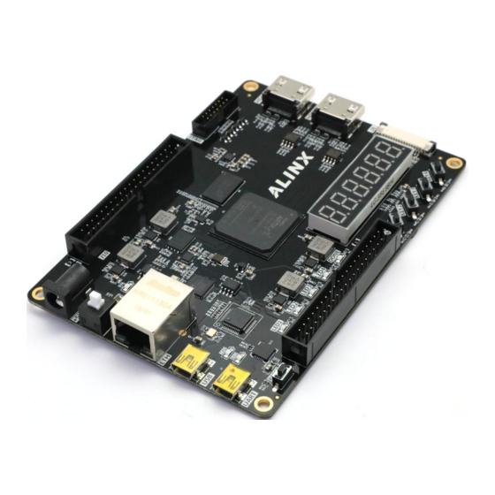
ARTIX-7 FPGA Development Board AX7035 User Manual Table of Contents Version Record .....................2 Part 1: FPGA Development Board Introduction .......... 5 Part 2: Structure Diagram ................8 Part 3: Power Supply ................... 9 Part 4: FPGA Chip ..................10 Part 5: 50M active crystal oscillator ............11 Part 6:DDR3 DRAM ................... - Page 4 ARTIX-7 FPGA Development Board AX7035 User Manual The AX7035 FPGA development board, it is the ARTIX-7 FPGA development platform. The ARTIX-7 FPGA development platform uses XILINX's ARTIX-7 chip, and theAX7035 FPGA development board are designed with a rich peripheral interface. For example, one HDMI input interface, one HDMI output interface, one Gigabit Ethernet interface, one USB2.0 interface, Uart interface,...
-
Page 5: Part 1: Fpga Development Board Introduction
A 128Mbit QSPI FLASH is used as an FPGA configuration chip to store FPGA configuration files and some user data. The AX7035 FPGA development board has expanded a wide range of peripheral interfaces, including one HDMI output interface, one HDMI input interface, one Gigabit Ethernet interface, one USB2.0 interface, one UART... - Page 6 ARTIX-7 FPGA Development Board AX7035 User Manual Figure 1-1: TheSchematic Diagram of the AX7035 Through this diagram, you can see the interfaces and functions that the AX7035FPGA Development Board contains: Xilinx ARTIX-7 Series FPGA Chip XC7A35T-2FGG484I A large-capacity 2Gbit (256MB) high-speed DDR3 SDRAM can be used as a buffer for FPGA chip data ...
- Page 7 2-channel40-pin expansion port Reserve 2 40-pin 2.54mm pitch expansion ports, which can be connected to various ALINX modules (binocular camera, TFT LCD screen, high-speed AD module, etc.). The expansion port contains 1 channel 5V power supply, 2 channel 3.3V power supply, 3 way ground, 34 IOs port.
-
Page 8: Part 2: Structure Diagram
ARTIX-7 FPGA Development Board AX7035 User Manual JTAG Interface A 10-pin0.1 spacing standard JTAG ports for FPGA program download and debugging. Key 1 reset key, 4 user keys LED Light 6LEDs, 1 power indicator, 1 DONE configuration indicator, 2 serial transmit and receive indicators, 4 user LEDs. -
Page 9: Part 3: Power Supply
ARTIX-7 FPGA Development Board AX7035 User Manual Part 3: Power Supply The power supply voltage of the AX7035 FPGA development board is DC5V, and Figure 3-1 is the power supply schematic: Figure 3-1: Power Supply Schematic The development board is powered by +5V and converted to +3.3V, +1.5V, +1.8V, +1.0V four-way power supply through four DC/DC power supply chip... -
Page 10: Part 4: Fpga Chip
ARTIX-7 FPGA Development Board AX7035 User Manual Power Supply Function +1.0V FPGACore VoltageVCCINT, VCCBRAM +1.8V FPGA auxiliary voltageVCCAUX, VCCBATT,ADC power supply VCCADC VCCIO ofFPGA, Ethernet, Serial port, HDMI, Sensor, FLASH, EEPROM, +3.3V and SD Card +1.5V DDR3, Bank34 of FPGA... -
Page 11: Part 5: 50M Active Crystal Oscillator
CCAUX each BANK of FPGA, including BANK0, BANK14~16, BANK34~35. On AX7035 FPGA development board, BANK34 need to be connected to DDR3, the voltage connection of BANK is 1.5V, and the voltage of other BANK is 3.3V. The V of BANK16 is powered by the LDO, and can be changed by replacing the LDO chip. -
Page 12: Part 6:Ddr3 Dram
ARTIX-7 FPGA Development Board AX7035 User Manual within the FPGA. The user can configure the FPGA's internal PLL and MMCM to achieve a higher clock. Figure 5-1: 50M active crystal oscillator Figure 5-2: 50M active crystal oscillator on the FPGA Board... - Page 13 ARTIX-7 FPGA Development Board AX7035 User Manual interface of the BANK 34 of the FPGA. The specific configuration of DDR3 SDRAM is shown in Table 6-1. Bit Number Chip Model Capacity Factory MT41J128M16HA-125 128M x 16bit Micron Table 6-1: DDR3 SDRAM Configuration The hardware design of DDR3 requires strict consideration of signal integrity.
- Page 14 ARTIX-7 FPGA Development Board AX7035 User Manual DDR3 DRAM pin assignment: Net Name FPGA PIN Name FPGA P/N DDR3_LDQS_P IO_L9P_T1_DQS_34 DDR3_LDQS_N IO_L9N_T1_DQS_34 DDR3_UDQS_P IO_L3P_T0_DQS_34 DDR3_UDQS_N IO_L3N_T0_DQS_34 DDR3_DQ[0] IO_L12P_T1_MRCC_34 DDR3_DQ [1] IO_L8N_T1_34 DDR3_DQ [2] IO_L8P_T1_34 DDR3_DQ [3] IO_L7P_T1_34 DDR3_DQ [4] IO_L10P_T1_34...
-
Page 15: Part 7: Qspi Flash
IO_L13P_T2_MRCC_34 Part 7: QSPI Flash The AX7035 FPGA development board is equipped with one128MBit QSPI FLASH, and the model is N25Q128, which uses the 3.3V CMOS voltage standard. Due to the non-volatile nature of QSPI FLASH, it can be used as a boot device for the system to store the boot image of the system. - Page 16 ARTIX-7 FPGA Development Board AX7035 User Manual Figure 7-1: QSPI Flash Schematic QSPI Flash pin assignments: Net Name FPGA PIN Name FPGA P/N QSPI_CLK CCLK_0 QSPI_CS IO_L6P_T0_FCS_B_14 QSPI_DQ0 IO_L1P_T0_D00_MOSI_14 QSPI_DQ1 IO_L1N_T0_D01_DIN_14 QSPI_DQ2 IO_L2P_T0_D02_14 QSPI_DQ3 IO_L2N_T0_D03_14 Figure 7-2: QSPI on the FPGA Board Amazon Store: https://www.amazon.com./alinx...
-
Page 17: Part 8: Gigabit Ethernet Interface
ARTIX-7 FPGA Development Board AX7035 User Manual Part 8: Gigabit Ethernet Interface The AX7035 development board provides network communication services to users through a Micrel KSZ9031RNX Ethernet PHY chip. The Ethernet PHY chip is connected to the IO interface of the ARTIX7 FPGA. The KSZ9031RNX chip supports 10/100/1000 Mbps network transmission rate and communicates with the FPGA through the RGMII interface. - Page 18 ARTIX-7 FPGA Development Board AX7035 User Manual Figure 8-1: Gigabit Ethernet Interface Schematic Figure 8-2: Gigabit Ethernet interface on the board Ethernet chip pin assignments are as follows: Signal Name FPGA Pin Description E1_GTXC RGMII transmit clock E1_TXD0 Transmit Data bit0...
-
Page 19: Part 9: Hdmi1 Output Interface
PHY Reset Signal Part 9: HDMI1 Output interface The implementation of the HDMI output interface on the AX7035 development board is to directly connect the differential signal and clock of the HDMI interface through the differential IO of the FPGA, realize the differential output of the HMDI signal after the data is encoded and parallel-to-differentially converted in the FPGA, and realize the HDMI digital video. - Page 20 ARTIX-7 FPGA Development Board AX7035 User Manual Figure 9-1: HDMI Output Interface Schematic When the development board is used as an output device for HDMI display, it needs to provide a +5V power supply to the HDMI display device. When the HDMI1_OUT_EN signal is high, it outputs +5V power to the external HDMI device.
- Page 21 ARTIX-7 FPGA Development Board AX7035 User Manual Figure 9-3: GTL2002D level conversion circuit Figure 9-4: HDMI Output Interface on the FPGA Board HDMI Output Pin Assignment Pin Name FPGA Pin HDMI1_CLK_P HDMI1_CLK_N HDMI1_D0_P HDMI1_D0_N HDMI1_D1_P HDMI1_D1_N HDMI1_D2_P HDMI1_D2_N HDMI1_SCL HDMI1_SDA...
-
Page 22: Part 10: Hdmi1 Input Interface (Also Used As An Output)
Part 10: HDMI1 input interface (also used as an output) The HDMI2 interface (J7) on the AX7035 development board can be used as both an HDMI input and an HDMI output. By default, the HDMI2 interface is used as an HDMI input. The data differential signal and clock signal of the HDMI interface are directly connected to the differential IO of the FPGA. - Page 23 ARTIX-7 FPGA Development Board AX7035 User Manual Figure 10-1: HDMI Input Interface Schematic When the development board is used as an input device for HDMI display, the power supply of HDMI1_5V is provided by the external main device. Here, the signal of HDMI2_OUT_EN needs to be set to low level, and the output of U20 chip is not enabled to be 5V.
- Page 24 ARTIX-7 FPGA Development Board AX7035 User Manual Figure 10-3: GTL2002D level conversion circuit Figure 10-4: HDMI Input Interface on the board HDMI Input Interface Pin Assignment Pin Name FPGA Pin HDMI2_CLK_P HDMI2_CLK_N HDMI2_D0_P HDMI2_D0_N HDMI2_D1_P HDMI2_D1_N HDMI2_D2_P HDMI2_D2_N HDMI2_SCL HDMI2_SDA...
-
Page 25: Part 11: Usb 2.0 Communication Interface
ARTIX-7 FPGA Development Board AX7035 User Manual Part 11: USB 2.0 Communication Interface In the AX7035 FPGA development board, usedFT232H single-channel high-speed USB chip of FEDI, to realize USB2.0 data communication between the FPGA development board and the computer. Maximum USB2.0 high-speed communication (480Mb/s) and full-speed communication (12Mb/s). -
Page 26: Part 12: Sd Card Slot
ARTIX-7 FPGA Development Board AX7035 User Manual Figure 11-2: USB 2.0 part on the FPGA Board USB 2.0 Pin Assignment Signal Name FPGA PIN Description USB_FD0 USB2.0 data Bit0 USB_FD1 USB2.0 data Bit1 USB_FD2 USB2.0 data Bit2 USB_FD3 USB2.0 data Bit3 USB_FD4 USB2.0 data Bit4... - Page 27 ARTIX-7 FPGA Development Board AX7035 User Manual substantial research and development. In 2000, these companies launched the SD Association (Secure Digital Association), which has a strong lineup and attracted a large number of vendors. These include IBM, Microsoft, Motorola, NEC, Samsung, and others.
-
Page 28: Part 13: Usb To Serial Port
SD_CD_N Part 13: USB to Serial Port The AX7035 FPGA development board includes the USB-UAR chip of Silicon Labs CP2102GM. The USB interface uses the MINI USB interface. It can be connected to the USB port of the upper PC for serial data communication with a USB cable. -
Page 29: Part 14: Eeprom 24Lc04
UART_TXD Part 14: EEPROM 24LC04 The AX7035 development board contains an EEPROM, model 24LC04, and has a capacity of 4Kbit (2*256*8bit). It consists of two 256-byte blocks and communicates via the IIC bus. The onboard EEPROM is to learn the Amazon Store: https://www.amazon.com./alinx... -
Page 30: Part 15: Digital Tube
EEPROM_I2C_SDA Part 15: Digital Tube The AX7035 development board has 6 digital tubes for displaying digital information. The digital tube we use is a 6-in-one eight-segment digital tube, and the segment structure of a digital tube is shown in Figure 15-1. - Page 31 ARTIX-7 FPGA Development Board AX7035 User Manual Figure 15-1: Segment structure of digital tube We use a common anode digital tube. When the corresponding pin of a certain field is low, the corresponding field is lit. When the corresponding pin of a certain field is high, the corresponding field is not lit.
- Page 32 ARTIX-7 FPGA Development Board AX7035 User Manual Figure 15-2: Digital Tube Schematic Figure 15-3: Digital Tube on the FPGA Board Digital tube pin assignment Pin Name FPGA Pin Description DIG0 Corresponding segment A DIG1 Corresponding segment B DIG2 Corresponding segment C...
-
Page 33: Part 16: Temperature Sensor
Part 16: Temperature Sensor A high-precision, low-power, digital temperature sensor chip is mounted on the AX7035 FPGA development board, and the model is LM75 of ON Semiconductor. The temperature accuracy of the LM75 chip is 0.5 degrees. The sensor and FPGA are directly connected to the I2C digital interface. The FPGA reads the temperature near the current FPGA development board through the I2C interface. -
Page 34: Part 17: Expansion Header
The AX7035 FPGA development board is reserved with two 0.1inch spacing standard 40-pin expansion headers J9 and J10. Which are used to connect the ALINX modules or the external circuit designed by the user.The signal of the expansion port J9 is connected to the BANK16 of the FPGA, so the LDO chip (U27) can be replaced to meet different level’s standard. - Page 35 ARTIX-7 FPGA Development Board AX7035 User Manual Figure 17-1: Expansion header J9 schematic Figure 17-2: Expansion header J9on the FPGABoard J9 Expansion Header Pin Assignment J9 Pin Number FPGA Pin J9 Pin Number FPGA Pin Amazon Store: https://www.amazon.com./alinx 35 / 42 Sales Email: rachel.zhou@aithtech.com...
- Page 36 ARTIX-7 FPGA Development Board AX7035 User Manual +3.3V +3.3V Figure 17-3: Expansion header J10 schematic Figure 17-4: Expansion header J10on the FPGA Board J10 Expansion Header Pin Assignment J10 Pin Number FPGA Pin J10 Pin Number FPGA Pin Amazon Store: https://www.amazon.com./alinx...
-
Page 37: Part 18: Fpc Expansion Ports
+3.3V Part 18: FPC Expansion Ports A 15-pin FPC expansion port J8 is reserved on the AX7035 FPGA development board, and an external module (such as a MIPI camera) is connected through a 15-line 1mm pitch FPC cable. The expansion port has 3 pairs of differential signals, 4 control signals, 1-channel 3.3V power supply... - Page 38 ARTIX-7 FPGA Development Board AX7035 User Manual Figure18-1: FPC Expansion Ports Schematic Figure18-2: FPC Expansion Ports on the FPGA Board FPC Expansion Ports Pin Assignment Pin Number Signal network name FPGA Pin MIPI_LAN0_N Amazon Store: https://www.amazon.com./alinx 38 / 42 Sales Email:...
-
Page 39: Part 19: Jtag Interface
+3.3V Part 19: JTAG Interface A JTAG interface is reserved JTAG interface one the AX7035 FPGA development board for downloading FPGA programs or firmware to FLASH. In order to prevent damage to the FPGA chip caused by hot plugging, a protection diode is added to the JTAG signal to ensure that the voltage of the signal is within the range accepted by the FPGA to avoid damage of the FPGA chip. -
Page 40: Part 20: User Keys
Be careful not to hot swap when JTAG cable is plugged and unplugged. Part 20: User Keys The AX7035 FPGA development board contains one reset key and four user keys KEY1~KEY4. All keys are connected to the normal IO of the FPGA. - Page 41 ARTIX-7 FPGA Development Board AX7035 User Manual The key is active low. When the key is pressed, the IO input voltage of the FPGA is low. When no key is pressed, The IO input voltage of the FPGA is high.
-
Page 42: Part 21: Led Light
ARTIX-7 FPGA Development Board AX7035 User Manual Part 21: LED Light There are seven red LEDs on the AX7035 FPGA development board, one of which is the power indicator (PWR), two are USB Uart data receiving and sending indicators, four are users LED lights (LED1~LED4). When the AX7035 FPGA board is powered on, the power indicator will light up;...
Need help?
Do you have a question about the AX7035 and is the answer not in the manual?
Questions and answers