Table of Contents
Advertisement
Quick Links
Advertisement
Table of Contents

Related Manuals for Alinx AX7A200


Summary of Contents for Alinx AX7A200
- Page 1 ARTIX-7 FPGA Development Board AX7A200 User Manual...
-
Page 2: Version Record
Date Release By Description Rev 1.0 2019-07-10 Rachel Zhou First Release The English version was translated by Shanghai Tianhui Trading Company. They has not been officially Review by ALINX and are for reference only. there errors, please send email rachel.zhou@aithtech.com for correction. -
Page 3: Table Of Contents
ARTIX-7 FPGA Development Board AX7A200 User Manual Table of Contents Version Record .....................2 Part 1: FPGA Development Board Introduction .......... 6 Part 2: AC7A200 Core Board ..............10 Part 2.1: AC7A200 Core Board Introduction ........10 Part 2.2: FPGA Chip ................12 Part 2.3: Active Differential Crystal .............13... - Page 4 ARTIX-7 FPGA Development Board AX7A200 User Manual Part 3.13: Buttons ................54 Part 3.14: LED Light ................55 Part 3.15: Power Supply ..............57 Part 3.16: Fan ..................58 Part 3.17: Carrier Board Form Factors ..........59 Amazon Store: https://www.amazon.com/alinx 4 / 59 Sales Email: rachel.zhou@aithtech.com...
- Page 5 ARTIX-7 FPGA Development Board AX7A200 User Manual This ARTIX-7 FPGA development platform adopts the core board + carrier board mode, which is convenient for users to use the core board for secondary development. In the design of carrier board, we have extended a wealth of interfaces for...
-
Page 6: Part 1: Fpga Development Board Introduction
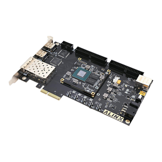
ARTIX-7 FPGA Development Board AX7A200 User Manual Part 1: FPGA Development Board Introduction The entire structure of the AX7A200 FPGA development board is inherited from our consistent core board + carrier board model. A high-speed inter-board connector is used between the core board and the carrier board. - Page 7 ARTIX-7 FPGA Development Board AX7A200 User Manual Figure 1-1-1: The Schematic Diagram of the AX7A200 Through this diagram, you can see the interfaces and functions that the AX7102 FPGA Development Board contains: Artix-7 FPGA core board The core board consists of XC7A200T + 8Gb DDR3 + 128Mb QSPI FLASH.
- Page 8 ARTIX-7 FPGA Development Board AX7A200 User Manual interfaces. Each fiber optic data communication receives and transmits at speeds up to 6.6 Gb/s. 1-channel Gigabit Ethernet Interface RJ-45 interface The Gigabit Ethernet interface chip uses Micrel's KSZ9031RNX Ethernet PHY chip to provide network communication services to users.
- Page 9 ARTIX-7 FPGA Development Board AX7A200 User Manual A 10-pin 0.1 inch spacing standard JTAG ports for FPGA program download and debugging. Button 4 buttons; 1 reset button (on the core board) LED Light 5 user LEDs (1 on the core board and 4 on the carrier board) Amazon Store: https://www.amazon.com/alinx...
-
Page 10: Part 2: Ac7A200 Core Board
ARTIX-7 FPGA Development Board AX7A200 User Manual Part 2: AC7A200 Core Board Part 2.1: AC7A200 Core Board Introduction AC7A200 (core board model, the same below) FPGA core board, it is based on XILINX's ARTIX-7 series 100T XC7A200T-2FBG484I. It is a high-performance core board with high speed, high bandwidth and high capacity. - Page 11 ARTIX-7 FPGA Development Board AX7A200 User Manual Figure 2-1-1: AC7A200 Core Board (Front View) Figure 2-1-2: AC7A200 Core Board (Rear View) Amazon Store: https://www.amazon.com/alinx 11 / 59 Sales Email: rachel.zhou@aithtech.com...
-
Page 12: Part 2.2: Fpga Chip
ARTIX-7 FPGA Development Board AX7A200 User Manual Part 2.2: FPGA Chip As mentioned above, the FPGA model we use is XC7A200T-2FBG484I, which belongs to Xilinx's Artix-7 series. The speed grade is 2, and the temperature grade is industry grade. This model is a FGG484 package with 484 pins. -
Page 13: Part 2.3: Active Differential Crystal
ARTIX-7 FPGA Development Board AX7A200 User Manual DSP Slices PCIe Gen2 XADC 1 XADC, 12bit, 1Mbps AD GTP Transceiver 4 GTP, 6.6Gb/s max Speed Grade Temperature Grade Industrial FPGA power supply system Artix-7 FPGA power supplies are V CCINT CCBRAM... - Page 14 ARTIX-7 FPGA Development Board AX7A200 User Manual model is SiT9102 -125MHz, reference clock input for GTP transceivers. Part 2.3.1: 200Mhz Active Differential clock G1 in Figure 2-3-1 is the 200M active differential crystal that provides the development board system clock source. The crystal output is connected to the BANK34 global clock pin MRCC (R4 and T4) of the FPGA.
- Page 15 ARTIX-7 FPGA Development Board AX7A200 User Manual Part 2.3.2: 125MHz Active Differential Crystal G2 in Figure 2-3-3 is the 125MHz active differential crystal, which is the reference input clock provided to the GTP module inside the FPGA. The crystal output is connected to the GTP BANK216 clock pins MGTREFCLK0P (F6) and MGTREFCLK0N (E6) of the FPGA.
-
Page 16: Part 2.4: Ddr3 Dram
ARTIX-7 FPGA Development Board AX7A200 User Manual Part 2.4: DDR3 DRAM The FPGA core board AC7A200 is equipped with two Micron 4Gbit (512MB) DDR3 chips (8Gbit in totally), model is MT41J256M16HA-125 (compatible with MT41K256M16HA-125). The DDR3 SDRAM has a maximum operating speed of 400MHz (data rate 800Mbps). - Page 17 ARTIX-7 FPGA Development Board AX7A200 User Manual Figure 2-4-2: The DDR3 on the Core Board DDR3 DRAM pin assignment: Net Name FPGA PIN Name FPGA P/N DDR3_DQS0_P IO_L3P_T0_DQS_AD5P_35 DDR3_DQS0_N IO_L3N_T0_DQS_AD5N_35 DDR3_DQS1_P IO_L9P_T1_DQS_AD7P_35 DDR3_DQS1_N IO_L9N_T1_DQS_AD7N_35 DDR3_DQS2_P IO_L15P_T2_DQS_35 DDR3_DQS2_N IO_L15N_T2_DQS_35 DDR3_DQS3_P IO_L21P_T3_DQS_35...
- Page 18 ARTIX-7 FPGA Development Board AX7A200 User Manual DDR3_DQ [12] IO_L7N_T1_AD6N_35 DDR3_DQ [13] IO_L10P_T1_AD15P_35 DDR3_DQ [14] IO_L7P_T1_AD6P_35 DDR3_DQ [15] IO_L12P_T1_MRCC_35 DDR3_DQ [16] IO_L18N_T2_35 DDR3_DQ [17] IO_L16P_T2_35 DDR3_DQ [18] IO_L14P_T2_SRCC_35 DDR3_DQ [19] IO_L17N_T2_35 DDR3_DQ [20] IO_L14N_T2_SRCC_35 DDR3_DQ [21] IO_L17P_T2_35 DDR3_DQ [22] IO_L13N_T2_MRCC_35...
-
Page 19: Part 2.5: Qspi Flash
ARTIX-7 FPGA Development Board AX7A200 User Manual DDR3_A[12] IO_L4N_T0_34 DDR3_A[13] IO_L1N_T0_34 DDR3_A[14] IO_L6N_T0_VREF_34 DDR3_BA[0] IO_L9N_T1_DQS_34 DDR3_BA[1] IO_L9P_T1_DQS_34 DDR3_BA[2] IO_L11P_T1_SRCC_34 DDR3_S0 IO_L8P_T1_34 DDR3_RAS IO_L12P_T1_MRCC_34 DDR3_CAS IO_L12N_T1_MRCC_34 DDR3_WE IO_L7P_T1_34 DDR3_ODT IO_L14N_T2_SRCC_34 DDR3_RESET IO_L15P_T2_DQS_34 DDR3_CLK_P IO_L3P_T0_DQS_34 DDR3_CLK_N IO_L3N_T0_DQS_34 DDR3_CKE IO_L14P_T2_SRCC_34 Part 2.5: QSPI Flash The FPGA core board AC7A200 is equipped with one 128Mbit QSPI FLASH, and the model is N25Q128, which uses the 3.3V CMOS voltage... - Page 20 ARTIX-7 FPGA Development Board AX7A200 User Manual Figure 2-5-1: QSPI Flash Schematic QSPI Flash pin assignments: Net Name FPGA PIN Name FPGA P/N QSPI_CLK CCLK_0 QSPI_CS IO_L6P_T0_FCS_B_14 QSPI_DQ0 IO_L1P_T0_D00_MOSI_14 QSPI_DQ1 IO_L1N_T0_D01_DIN_14 QSPI_DQ2 IO_L2P_T0_D02_14 QSPI_DQ3 IO_L2N_T0_D03_14 Figure 2-5-1: QSPI FLASH on the Core Board Amazon Store: https://www.amazon.com/alinx...
-
Page 21: Part 2.6: Led Light On Core Board
ARTIX-7 FPGA Development Board AX7A200 User Manual Part 2.6: LED Light on Core Board There are 3 red LED lights on the AC7A200 FPGA core board, one of which is the power indicator light (PWR), one is the configuration LED light (DONE), and one is the user LED light. -
Page 22: Part 2.7: Jtag Interface
ARTIX-7 FPGA Development Board AX7A200 User Manual Figure 2-6-2: LED lights on the Core Board User LEDs Pin Assignment Signal Name FPGA Pin Name FPGA Pin Number Description LED1 IO_L15N_T2_DQS_34 User LED Part 2.7: JTAG Interface The JTAG test socket J1 is reserved on the AC7A200 core board for JTAG download and debugging when the core board is used alone. -
Page 23: Part 2.8: Power Interface On The Core Board
ARTIX-7 FPGA Development Board AX7A200 User Manual GND, +3.3V these six signals. Figure 2-7-1: JTAG Interface Schematic The JTAG interface J1 on AC7A200 FPGA core board uses a 6-pin 2.54mm pitch single-row test hole. If you need to use the JTAG connector to debug on the core board, you need to solder a 6-pin single-row pin header. -
Page 24: Part 2.9: Board To Board Connectors Pin Assignment
ARTIX-7 FPGA Development Board AX7A200 User Manual Figure 2-8-1:Power Interface schematic on the Core Board Figure 2-8-2:Power interface on the Core Board Part 2.9: Board to Board Connectors pin assignment The core board has a total of four high-speed board to board connectors. - Page 25 ARTIX-7 FPGA Development Board AX7A200 User Manual Pin Assignment of Board to Board Connectors CON1 CON1 FPGA Voltage CON1 FPGA Voltage Name Level Name Level PIN1 VCCIN PIN2 VCCIN PIN3 VCCIN PIN4 VCCIN PIN5 VCCIN PIN6 VCCIN PIN7 VCCIN PIN8...
- Page 26 ARTIX-7 FPGA Development Board AX7A200 User Manual PIN61 B16_L1_N 3.3V PIN62 PIN63 B16_L1_P 3.3V PIN64 PIN65 B16_L4_N 3.3V PIN66 PIN67 B16_L4_P 3.3V PIN68 PIN69 Ground PIN70 Ground PIN71 B16_L6_N 3.3V PIN72 PIN73 B16_L6_P 3.3V PIN74 PIN75 B16_L8_P 3.3V PIN76 PIN77 B16_L8_N 3.3V...
- Page 27 ARTIX-7 FPGA Development Board AX7A200 User Manual PIN15 B13_L12_P 3.3V PIN16 B14_L8_N AA21 3.3V PIN17 B13_L12_N 3.3V PIN18 B14_L8_P AA20 3.3V PIN19 Ground PIN20 Ground PIN21 B13_L11_P 3.3V PIN22 B14_L15_N AB20 3.3V PIN23 B13_L11_N 3.3V PIN24 B14_L15_P AA19 3.3V PIN25 B13_L10_P 3.3V...
- Page 28 ARTIX-7 FPGA Development Board AX7A200 User Manual Figure 2-9-2: Board to Board Connectors CON2 on the Core Board Board to Board Connectors CON3 The 80-pin connector CON3 is used to extend the normal IO of the BANK15 and BANK16 of the FPGA. In addition, four JTAG signals are also connected to the carrier board via the CON3 connector.
- Page 29 ARTIX-7 FPGA Development Board AX7A200 User Manual PIN33 B15_L5_N 3.3V PIN34 B15_L7_P 3.3V PIN35 B15_L3_N 3.3V PIN36 B15_L9_P 3.3V PIN37 B15_L3_P 3.3V PIN38 B15_L9_N 3.3V PIN39 Ground PIN40 Ground PIN41 B15_L19_P 3.3V PIN42 B15_L15_N 3.3V PIN43 B15_L19_N 3.3V PIN44 B15_L15_P 3.3V...
- Page 30 ARTIX-7 FPGA Development Board AX7A200 User Manual Board to Board Connectors CON4 The 80-Pin connector CON4 is used to extend the normal IO and GTP high-speed data and clock signals of the FPGA BANK16. The voltage standard of the IO port of BANK16 can be adjusted by an LDO chip. The default installed LDO is 3.3V.
-
Page 31: Part 2.10: Power Supply
ARTIX-7 FPGA Development Board AX7A200 User Manual PIN43 B16_L5_N 3.3V PIN44 B16_L2_N 3.3V PIN45 B16_L7_P 3.3V PIN46 B16_L3_P 3.3V PIN47 B16_L7_N 3.3V PIN48 B16_L3_N 3.3V PIN49 Ground PIN50 Ground PIN51 B16_L9_P 3.3V PIN52 B16_L10_P 3.3V PIN53 B16_L9_N 3.3V PIN54 B16_L10_N 3.3V... - Page 32 ARTIX-7 FPGA Development Board AX7A200 User Manual Figure 2-10-1:Power Supply on core board schematic The core board is powered by +5V and converted to +3.3V, +1.5V, +1.8V, +1.0V four-way power supply through three DC/DC power supply chip TLV62130RGT. The current of +1.0V can be up to 6A, and the other three output currents can be up to 3A.
- Page 33 ARTIX-7 FPGA Development Board AX7A200 User Manual Power Supply Function +1.0V FPGA Core Voltage +1.8V FPGA auxiliary voltage, TPS74801 power supply +3.3V VCCIO of Bank0,Bank13 and Bank14 of FPGA,QSIP FLASH, Clock Crystal +1.5V DDR3, Bank34 and Bank35 of FPGA VREF,VTT(+0.75V) DDR3 CCIP(+3.3V)
-
Page 34: Part 2.11: Core Board Form Factors
ARTIX-7 FPGA Development Board AX7A200 User Manual Part 2.11: Core Board Form Factors Figure 2-11-1: AC7A200 FPGA Core board (Top view) Figure 2-11-2: AC7A200 FPGA Core board (Bottom view) Amazon Store: https://www.amazon.com/alinx 34 / 59 Sales Email: rachel.zhou@aithtech.com... -
Page 35: Part 3: Carrier Board
ARTIX-7 FPGA Development Board AX7A200 User Manual Part 3: Carrier Board Part 3.1: Carrier Board Introduction Through the previous function introduction, you can understand the function of the carrier board part 1-channel PCIe x2 high speed data transmission interface ... -
Page 36: Part 3.2: Gigabit Ethernet Interface
ARTIX-7 FPGA Development Board AX7A200 User Manual Part 3.2: Gigabit Ethernet Interface The AX7A200 FPGA development board provides users with 1-channel Gigabit network communication service through the Micrel KSZ9031RNX Ethernet PHY chip. The Ethernet PHY chip is connected to the IO interface of the ARTIX7 FPGA. - Page 37 ARTIX-7 FPGA Development Board AX7A200 User Manual Figure 3-2-1: Gigabit Ethernet Interface Schematic Figure 3-3-2: Gigabit Ethernet interface on the Carrier board Gigabit Ethernet Chip PHY pin assignments are as follows: Signal Name FPGA Pin Number Description RGMII transmit clock...
-
Page 38: Part 3.3: Sfp Interface
PHY Chip Reset Signal ETH_RESET Part 3.3: SFP Interface The AX7A200 FPGA development board has two optical interfaces. Users can purchase SFP optical modules (1.25G, 2.5G optical modules on the market) and insert them into these two optical interfaces for optical data communication. - Page 39 ARTIX-7 FPGA Development Board AX7A200 User Manual Figure 3-3-2: SFP interfaces on the Carrier Board The 1 fiber interface FPGA pin assignment is as follows: Signal Name FPGA PIN Description SFP1_TX_P SFP1 Data Transfer (Positive) SFP1_TX_N SFP1 Data Transfer (Negative)
-
Page 40: Part 3.4: Pcie X2 Interface
RX signals are connected to the FPGA in differential signals, and the single channel communication rate can be up to 5G bit bandwidth. The PCIe reference clock is provided to the AX7A200 FPGA development board by the PCIe slot of the PC with a reference clock frequency of 100Mhz. -
Page 41: Part 3.5: Hdmi Output Interface
ARTIX-7 FPGA Development Board AX7A200 User Manual PCIex2 Interface Pin Assignment: Signal Name FPGA Pin Description PCIE Channel 0 Data Receive Positive PCIE_RX0_P PCIE Channel 0 Data Receive Negative PCIE_RX0_N PCIE Channel 1 Data Receive Positive PCIE_RX1_P PCIE Channel 1 Data Receive Negative... - Page 42 ARTIX-7 FPGA Development Board AX7A200 User Manual Figure 3-5-1: HDMI Output on the Carrire Board HDMI Input Pin Assignment: Signal Name FPGA Pin 9134_NRESET 9134_CLK 9134_HS 9134_VS 9134_DE 9134_D[0] 9134_D[1] 9134_D[2] 9134_D[3] 9134_D[4] 9134_D[5] 9134_D[6] 9134_D[7] 9134_D[8] 9134_D[9] 9134_D[10] 9134_D[11]...
-
Page 43: Part 3.6: Hdmi Input Interface
ARTIX-7 FPGA Development Board AX7A200 User Manual 9134_D[17] AB22 9134_D[18] AB21 9134_D[19] 9134_D[20] 9134_D[21] 9134_D[22] 9134_D[23] HDMI_SCL HDMI_SDA Part 3.6: HDMI Input interface HDMI output interface, select Silion Image's SIL9013/9011 HDMI decoder chip, support up to 1080P@60Hz input and support data output in different formats. - Page 44 ARTIX-7 FPGA Development Board AX7A200 User Manual Figure 3-6-2: HDMI Input on the Carrier Board HDMI Input Pin Assignment: Signal Name FPG Pin Number 9013_NRESET 9013_CLK 9013_HS 9013_VS 9013_DE 9013_D[0] 9013_D[1] 9013_D[2] 9013_D[3] 9013_D[4] 9013_D[5] 9013_D[6] 9013_D[7] 9013_D[8] 9013_D[9] 9013_D[10]...
-
Page 45: Part 3.7: Sd Card Slot
ARTIX-7 FPGA Development Board AX7A200 User Manual 9013_D[16] 9013_D[17] 9013_D[18] 9013_D[19] 9013_D[20] 9013_D[21] 9013_D[22] 9013_D[23] HDMI_SCL HDMI_SDA Part 3.7: SD Card Slot The SD card (Secure Digital Memory Card) is a memory card based on the semiconductor flash memory process. It was... -
Page 46: Part 3.8: Usb-To-Uart Bridge Connector
SD_DAT3 Part 3.8: USB-to-Uart Bridge Connector The AX7A200 FPGA development board includes the USB-UAR chip of Silicon Labs CP2102GM. The USB interface uses the MINI USB interface. It can be connected to the USB port of the upper PC for serial data communication with a USB cable. - Page 47 ARTIX-7 FPGA Development Board AX7A200 User Manual Figure 3-8-1: USB to serial port schematic Figure 3-8-2: USB to serial port on the Carrier Board Two LED indicators (LED3 and LED4) are set for the serial port signal, and the silkscreen on the PCB is TX and RX, indicating that the serial port has data...
-
Page 48: Part 3.9: Eeprom 24Lc04
UART1_TXD Part 3.9: EEPROM 24LC04 AX7A200 carrier board contains an EEPROM, model 24LC04, and has a capacity of 4Kbit (2*256*8bit). It consists of two 256-byte blocks and communicates via the IIC bus. The onboard EEPROM is to learn how to communicate with the IIC bus. -
Page 49: Part 3.10: Temperature Sensor
Part 3.10: Temperature Sensor A high-precision, low-power, digital temperature sensor chip is mounted on the AX7A200 FPGA development board, and the model is LM75 of ON Semiconductor. The temperature accuracy of the LM75 chip is 0.5 degrees, I2C bus is shared with EEPROM. The sensor and FPGA are directly connected to the I2C digital interface. -
Page 50: Part 3.11: Expansion Header
Part 3.11: Expansion Header The carrier board is reserved with two 0.1inch spacing standard 40-pin expansion ports J11 and J13, which are used to connect the ALINX modules or the external circuit designed by the user. The expansion port has 40 signals, of which 1-channel 5V power supply, 2-channel 3.3 V power supply, 3-channle... - Page 51 ARTIX-7 FPGA Development Board AX7A200 User Manual The figure 3-11-2 detailed the J11 expansion port on the carrier board. The Pin1 and Pin2 of the expansion port are already marked on the board. Figure 3-11-2: Expansion header J11 on the Carrier Board...
- Page 52 ARTIX-7 FPGA Development Board AX7A200 User Manual Figure 3-11-3: Expansion header J13 schematic The figure 3-11-4 detailed the J13 expansion port on the carrier board. The Pin1 and Pin2 of the expansion port are already marked on the board. Figure 3-11-4: Expansion header J13 on the carrier board...
-
Page 53: Part 3.12: Jtag Interface
ARTIX-7 FPGA Development Board AX7A200 User Manual AA10 AA11 AB10 AA13 AB13 AB11 AB12 AA14 AA16 AB16 AB17 AA15 AB15 +3.3V +3.3V Part 3.12: JTAG Interface The development board reserves a JTAG interface for downloading FPGA programs or firmware to FLASH. In order to prevent damage to the FPGA chip... -
Page 54: Part 3.13: Buttons
Figure 3-12-2: JTAG Interface on the Carrier Board Part 3.13: Buttons The AX7A200 FPGA carrier board contains five user buttons RESET, KEY1~KEY4, and all the buttons are connected to the normal IO of the FPGA. The button is active low. When the button is pressed, the IO input voltage of the FPGA is low. -
Page 55: Part 3.14: Led Light
KEY1 KEY2 KEY3 KEY4 Part 3.14: LED Light There are seven red LEDs on the AX7A200 FPGA carrier board, one of which is the power indicator (PWR), two are USB Uart data receiving and Amazon Store: https://www.amazon.com/alinx 55 / 59 Sales Email: rachel.zhou@aithtech.com... - Page 56 ARTIX-7 FPGA Development Board AX7A200 User Manual transmitting indicators, and four are users LED lights (LED1~LED4). When the board is powered on, the power indicator will light up; User LED1~LED4 are connected to the normal IO of the FPGA. When the IO voltage connected to the user LED is configured low level, the user LED lights up.
-
Page 57: Part 3.15: Power Supply
ARTIX-7 FPGA Development Board AX7A200 User Manual Part 3.15: Power Supply The power input voltage of the AX7A200 FPGA development board is DC12V. The development board also supports power from the PCIe interface. +12V Powered by Power adapter Powered by... -
Page 58: Part 3.16: Fan
ARTIX-7 FPGA Development Board AX7A200 User Manual Figure 3-15-3: Power Supply Circuit on the Carrier Board Part 3.16: Fan Because the FPGA chip generates a lot of heat when it works normally, we add a heat sink and fan to the chip to prevent the chip from overheating. The fan is controlled by the FPGA chip. -
Page 59: Part 3.17: Carrier Board Form Factors
ARTIX-7 FPGA Development Board AX7A200 User Manual The fan has been screwed to the development board before leaving the factory. The power of the fan is connected to the J8 socket. The red is positive and the black is negative.
Need help?
Do you have a question about the AX7A200 and is the answer not in the manual?
Questions and answers