Alinx ZYNQ7000 FPGA User Manual
Hide thumbs
Also See for ZYNQ7000 FPGA:
- User manual (61 pages) ,
- User manual (48 pages) ,
- User manual (53 pages)
Table of Contents
Advertisement
Advertisement
Table of Contents

Subscribe to Our Youtube Channel
Related Manuals for Alinx ZYNQ7000 FPGA


Summary of Contents for Alinx ZYNQ7000 FPGA
- Page 1 ZYNQ7000 FPGA Development Board AX7Z010 User Manual...
-
Page 2: Version Record
ZYNQ FPGA Development Board AX7Z010 User Manual Version Record Version Date Release By Description Rev 1.0 2019-12-15 Rachel Zhou First Release Amazon Store: https://www.amazon.com/alinx 2 / 54... -
Page 3: Table Of Contents
Part 3.10: SD Card Slot Interface ............. 42 Part 3.11: EEPROM ................. 43 Part 3.12: Real-time clock ..............44 Part 3.13: Temperature sensor ............45 Part 3.14: JTAG Debug Port ............. 46 Part 3.15: User LEDs ............... 47 Amazon Store: https://www.amazon.com/alinx 3 / 54... - Page 4 ZYNQ FPGA Development Board AX7Z010 User Manual Part 3.16: User Keys ................ 48 Part 3.17: Expansion Header ............49 Part 3.18: Power Supply ..............52 Part 3.19: Carrier Board Size Dimension .......... 54 Amazon Store: https://www.amazon.com/alinx 4 / 54...
- Page 5 ZYNQ FPGA Development Board AX7Z010 User Manual This ZYNQ7000 FPGA development platform adopts the core board + carrier board mode, which is convenient for users to use the core board for secondary development. The core board uses XILINX's Zynq7000 SOC chip XC7Z010 solution, uses ARM+FPGA SOC technology to integrate dual-core ARM Cortex-A9 and FPGA programmable logic on a single chip.
- Page 6 ZYNQ FPGA Development Board AX7Z010 User Manual Amazon Store: https://www.amazon.com/alinx 6 / 54...
-
Page 7: Part 1: Fpga Development Board Introduction
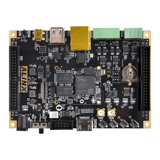
1 UART USB interface. 1 SD card slot, 2-Channel CAN bus interfaces, 2-Channel RS485 bus interfaces, 2-Channel AD input interface, 2-Channel 40-pin expansion header, some keys and LEDs. The following figure shows the structure of the entire development system: Amazon Store: https://www.amazon.com/alinx 7 / 54... - Page 8 33.333333MHz crystal oscillator provides the clock to the PS system. CAN Communication Interface 2 CAN bus interface, using SN65HVD232 chip from TI Company. 485 Communication Interface 2-Channel 485 communication interfaces, using MAX3485 chip of MAXIM Company. Amazon Store: https://www.amazon.com/alinx 8 / 54...
- Page 9 Temperature and humidity sensor chip LM75 On-board temperature and humidity sensor chip LM75, used to detect the temperature and humidity of the surrounding environment around the FPGA development board 1 MIPI camera interface Amazon Store: https://www.amazon.com/alinx 9 / 54...
- Page 10 ZYNQ FPGA Development Board AX7Z010 User Manual It can be used to connect ALINX OV5640 camera with MIPI interface (only for AX7Z020). JTAG debug port A 10-pin 0.1 spacing standard JTAG ports for FPGA program download and debugging. Users can debug and download the ZYNQ system through the XILINX downloader.
-
Page 11: Part 2: Ac7Z010 Core Board
And the IO connection part, the ZYNQ chip to the interface between the equal length and differential processing, and the core board size is only 35 * 42 (mm), which is very suitable for secondary development. Amazon Store: https://www.amazon.com/alinx 11 / 54... - Page 12 ZYNQ FPGA Development Board AX7Z010 User Manual Figure 2-1-1: AC7Z010 Core Board (Front View) Figure 2-1-2: AC7Z100 Core Board (Rear View) Amazon Store: https://www.amazon.com/alinx 12 / 54...
-
Page 13: Part 2.2: Zynq Chip
The main parameters of the PS system part are as follows: ARM dual-core CortexA9-based application processor, ARM-v7 architecture, up to 800MHz 32KB level 1 instruction and data cache per CPU, 512KB level 2 cache 2 CPU shares Amazon Store: https://www.amazon.com/alinx 13 / 54... - Page 14 17 external differential input channels, 1MBPS XC7Z100-1CLG400I chip speed grade is -1, industrial grade, package is BGA400, pin pitch is 0.8mm the specific chip model definition of ZYNQ7000 series is shown in Figure 2-2-2 Amazon Store: https://www.amazon.com/alinx 14 / 54...
-
Page 15: Part 2.3: Ddr3 Dram
The FPGA core board AC7Z010 is equipped with two Micron DDR3 SDRAM chips (1GB in total), model MT41K128M16TW-107 (Compatible with Hynix H5TQ2G63AFR-PBI). The total bus width of DDR3 SDRAM is 32bit. DDR3 SDRAM operates at a maximum speed of 533MHz (data rate Amazon Store: https://www.amazon.com/alinx 15 / 54... - Page 16 PCB design to ensure high-speed and stable operation of DDR3. The hardware connection of DDR3 DRAM is shown in Figure 2-3-1: Figure 2-3-1: DDR3 DRAM schematic diagram Amazon Store: https://www.amazon.com/alinx 16 / 54...
- Page 17 PS_DDR_DQS_N0_502 DDR3_DQS0_N PS_DDR_DQS_P1_502 DDR3_DQS1_P PS_DDR_DQS_N1_502 DDR3_DQS1_N PS_DDR_DQS_P2_502 DDR3_DQS2_P PS_DDR_DQS_N2_502 DDR3_DQS2_N PS_DDR_DQS_P3_502 DDR3_DQS3_P PS_DDR_DQS_N3_502 DDR3_DQS4_N PS_DDR_DQ0_502 DDR3_D0 PS_DDR_DQ1_502 DDR3_D1 PS_DDR_DQ2_502 DDR3_D2 PS_DDR_DQ3_502 DDR3_D3 PS_DDR_DQ4_502 DDR3_D4 PS_DDR_DQ5_502 DDR3_D5 PS_DDR_DQ6_502 DDR3_D6 PS_DDR_DQ7_502 DDR3_D7 PS_DDR_DQ8_502 DDR3_D8 PS_DDR_DQ9_502 DDR3_D9 Amazon Store: https://www.amazon.com/alinx 17 / 54...
- Page 18 PS_DDR_DQ29_502 DDR3_D29 PS_DDR_DQ30_502 DDR3_D30 PS_DDR_DQ31_502 DDR3_D31 PS_DDR_DM0_502 DDR3_DM0 PS_DDR_DM1_502 DDR3_DM1 PS_DDR_DM2_502 DDR3_DM2 PS_DDR_DM3_502 DDR3_DM3 PS_DDR_A0_502 DDR3_A0 PS_DDR_A1_502 DDR3_A1 PS_DDR_A2_502 DDR3_A2 PS_DDR_A3_502 DDR3_A3 PS_DDR_A4_502 DDR3_A4 PS_DDR_A5_502 DDR3_A5 PS_DDR_A6_502 DDR3_A6 PS_DDR_A7_502 DDR3_A7 PS_DDR_A8_502 DDR3_A8 PS_DDR_A9_502 DDR3_A9 Amazon Store: https://www.amazon.com/alinx 18 / 54...
-
Page 19: Part 2.4: Qspi Flash
Winbond Table 2-4-1: QSPI FLASH Specification QSPI FLASH is connected to the GPIO port of the BANK500 in the PS section of the ZYNQ chip. In the system design, the GPIO port functions of Amazon Store: https://www.amazon.com/alinx 19 / 54... - Page 20 Figure 2-4-2 is the QSPI Flash on the core board Configure chip pin assignments: Signal Name ZYNQ Pin Name ZYNQ Pin Number PS_MIO6_500 QSPI_SCK PS_MIO1_500 QSPI_CS PS_MIO2_500 QSPI_D0 PS_MIO3_500 QSPI_D1 PS_MIO4_500 QSPI_D2 PS_MIO5_500 QSPI_D3 Amazon Store: https://www.amazon.com/alinx 20 / 54...
-
Page 21: Part 2.5: Clock Configuration
ZYNQ Pin Signal name PS_CLK_500 Part 2.6: Power Supply The power supply voltage of the AC7Z010 core board is DC5V, which is supplied by connecting the carrier board. In addition, the power of BANK34 and Amazon Store: https://www.amazon.com/alinx 21 / 54... - Page 22 Power Supply Function +1.0V ZYNQ PS and PL section Core Voltage ZYNQ PS and PL partial auxiliary voltage +1.8V BANK501 IO voltage ZYNQ Bank0,Bank500,QSIP FLASH +3.3V Clock Crystal Amazon Store: https://www.amazon.com/alinx 22 / 54...
- Page 23 3.3V. When you design the carrier board to provide the VCCIO34 and VCCIO35 power for the core board, the power-on sequence is slower than + Amazon Store: https://www.amazon.com/alinx 23 / 54...
-
Page 24: Part 2.7: Ac7Z010 Core Board Size Dimension
BANK34 and BANK35 can be changed by adjusting the VCCIO input on the connector, the highest level does not exceed 3.3V. The AX7Z010 carrier board we designed is 3.3V by default. Note that the IO of BANK13 is not Amazon Store: https://www.amazon.com/alinx 24 / 54... - Page 25 VCCIO_34 VCCIO_35 IO34_L10P IO34_L7P IO34_L10N IO34_L7N IO34_L15N IO34_L17P IO34_L15P IO34_L17N IO34_L9N IO34_L8P IO34_L9P IO34_L8N IO34_L12N IO34_L3P IO34_L12P IO34_L3N IO34_L14N IO34_L21N IO34_L14P IO34_L21P IO34_L16N IO34_L18P IO34_L16P IO34_L18N IO34_L22N IO34_L23P IO34_L22P IO34_L23N IO34_L20N IO34_L13N IO34_L20P IO34_L13P Amazon Store: https://www.amazon.com/alinx 25 / 54...
- Page 26 IO13_L20N IO13_L18P IO13_L12N IO13_L18N IO13_L12P FPGA_TCK FPGA_TMS FPGA_TDO PS_POR_B FPGA_TDI FPGA_DONE Pin assignment of board to board connector J30 ZYNQ Pin ZYNQ J30 Pin Signal Name J30 Pin Signal Name Number Number IO35_L1P IO35_L15N Amazon Store: https://www.amazon.com/alinx 26 / 54...
- Page 27 IO35_L17P IO35_L16P IO35_L19N IO35_L13N IO35_L19P IO35_L13P IO35_L12N IO35_L14N IO35_L12P IO35_L14P IO35_L24N IO35_L20P IO35_L24P IO35_L20N IO35_L21N IO35_L11P IO35_L21P IO35_L11N IO35_L22N IO35_L23P IO35_L22P IO35_L23N PS_MIO22 PS_MIO50 PS_MIO27 PS_MIO45 PS_MIO23 PS_MIO46 PS_MIO24 PS_MIO41 PS_MIO25 PS_MIO7 PS_MIO26 PS_MIO12 Amazon Store: https://www.amazon.com/alinx 27 / 54...
- Page 28 PS_MIO20 PS_MIO9 PS_MIO19 PS_MIO14 PS_MIO18 PS_MIO8 PS_MIO17 PS_MIO0 PS_MIO39 PS_MIO13 PS_MIO38 PS_MIO47 PS_MIO37 PS_MIO48 PS_MIO28 PS_MIO49 PS_MIO35 PS_MIO52 PS_MIO34 PS_MIO51 PS_MIO33 PS_MIO40 PS_MIO32 PS_MIO44 PS_MIO31 PS_MIO15 PS_MIO36 PS_MIO42 PS_MIO29 PS_MIO43 PS_MIO30 PS_MIO53 QSPI_D3_PS_MIO5 QSPI_D2_PS_MIO4 Amazon Store: https://www.amazon.com/alinx 28 / 54...
-
Page 29: Part 3: Carrier Board
There are 2 CAN communication interfaces on the AX7Z010 carrier board, which are connected to the GPIO interface of the BANK500 on the PS system side. The CAN transceiver chip selected TI's SN65HVD232C chip for user CAN communication services. Amazon Store: https://www.amazon.com/alinx 29 / 54... - Page 30 Figure 3-2-2: CAN chip and interface of PS side on the carrier board The CAN communication pin assignments are as follows: Signal Name ZYNQ Pin Name ZYNQ Pin Number Description CAN0_RX PS_MIO10 CAN0 Receiver CAN0_TX PS_MIO11 CAN0 Transmitter CAN1_RX PS_MIO13 CAN1 Receiver CAN1_TX PS_MIO12 CAN1 Transmitter Amazon Store: https://www.amazon.com/alinx 30 / 54...
-
Page 31: Part 3.3: 485 Communication Interface
Figure 3-3-1 is the connection diagram of the 485 transceiver chip on the PL side 485_RXD1 MAX3485 485_TXD1 485_DE1 BANK ZYNQ 485_RXD2 MAX3485 485_TXD2 485_DE2 Figure 3-3-1: RS485 chip and interface connection diagram Figure 3-3-2: RS485 chip and interface on the carrier board Amazon Store: https://www.amazon.com/alinx 31 / 54... -
Page 32: Part 3.4: Gigabit Ethernet Interface
Enable 125Mhz clock output selection Enable LED_MODE LED light mode configuration Single LED light mode 10/100/1000 adaptive, compatible Link adaptation and full duplex MODE0~MODE3 with full-duplex, half-duplex configuration Table 3-4-1: PHY chip default configuration value Amazon Store: https://www.amazon.com/alinx 32 / 54... - Page 33 PHY1_TXCK PHY1_TXCTL PHY1_TXD0~PHY1_TXD3 PHY1_RXCK ZYNQ BANK GPHY PHY1_RXCTL (KSZ9031RNX) PHY1_TXD0~PHY1_RXD3 PHY1_MDC PHY1_MDIO PS_POR_B Figure 3-4-1: ZYNQ PS system and GPHY connection diagram Figure 3-4-2: Ethernet GPHY chip and interface on the carrier board Amazon Store: https://www.amazon.com/alinx 33 / 54...
-
Page 34: Part 3.5: Usb2.0 Host Interface
The USB port is flat USB ports (USB Type A), which allows users to connect different USB Slave peripherals (such as USB mouse and USB keyboard) at the same time. In addition, the carrier board provides + 5V power for the USB port. Amazon Store: https://www.amazon.com/alinx 34 / 54... - Page 35 USB Stop Signal OTG_NXT PS_MIO31 USB Next Data Signal OTG_DATA0 PS_MIO32 USB Data Bit0 OTG_DATA1 PS_MIO33 USB Data Bit1 OTG_DATA2 PS_MIO34 USB Data Bit2 OTG_DATA3 PS_MIO35 USB Data Bit3 OTG_CLK PS_MIO36 USB Clock Signal Amazon Store: https://www.amazon.com/alinx 35 / 54...
-
Page 36: Part 3.6: Usb To Serial Port
The schematic diagram of the USB Uart circuit design is shown in Figure 3-6-1: UART_TX VBUS BANK ZYNQ UART-USB 电平转换 REGIN UART_RX (TXS0102) (CP2102-GM) D+/- MINI USB Figure 3-6-1: USB to serial port schematic Figure 3-6-2: USB to serial port on the AX7Z010 Carrier Board Amazon Store: https://www.amazon.com/alinx 36 / 54... -
Page 37: Part 3.7: Ad Input Interface
ZYNQ. The schematic diagram of the AD acquisition circuit design is shown in Figure 3-7-1 below: AD1_P AD1_N AD9_P AD9_N ZYNQ BANK AD12_P AD12_N SNS5V+ BANK0 INA199 SNS5V- Figure 3-7-1: AD acquisition circuit Schematic Amazon Store: https://www.amazon.com/alinx 37 / 54... -
Page 38: Part 3.8: Hdmi Output Interface
The highest support 1080P @ 60Hz input and output function. The HDMI signal is connected to BANK34 in the PL part of ZYNQ. The schematic diagram of the design is shown in Figure 3-8-1 below: Amazon Store: https://www.amazon.com/alinx 38 / 54... - Page 39 ZYNQ FPGA Development Board AX7Z010 User Manual Figure 3-8-1: HDMI Output Interface Design Schematic Figure 3-8-2: HDMI Output Interface on the carrier board Amazon Store: https://www.amazon.com/alinx 39 / 54...
-
Page 40: Part 3.9: Mipi Camera Interface (Only For Ax7Z020)
AX7Z020) The AX7Z010 carrier board includes a MIPI camera interface, which can be used to connect with the ALINX Brand MIPI OV5640 camera module. The circuit schematic of the MIPI interface part is shown in Figure 3-9-1 below: Figure 3-9-1: MIPI camera interface design schematic Amazon Store: https://www.amazon.com/alinx... - Page 41 LANE1 negative in High Speed mode CAM_GPIO IO13_L11P GPIO control of camera module CAM_CLK IO13_L11N Clock input of camera module CAM_SCL IO13_L19P I2C clock of camera module CAM_SDA IO13_L19N I2C data of camera module Amazon Store: https://www.amazon.com/alinx 41 / 54...
-
Page 42: Part 3.10: Sd Card Slot Interface
SD card is 3.3V, connected through the TXS02612 level shifter. The schematic of the Zynq7000 PS and SD card connector is shown in Figure 3-10-1: Figure 3-10-1: SD Card Connection Diagram Figure 3-10-12: SD Card Interface on the carrier board Amazon Store: https://www.amazon.com/alinx 42 / 54... -
Page 43: Part 3.11: Eeprom
EEPROM is connected to the I2C interface of the ZYNQ PS end. Figure 3-11-1 is the connection diagram of EEPROM I2C_SCL_1V8 I2C_SCL BANK ZYNQ EEPROM 电平转换 I2C_SDA_1V8 I2C_SDA (TXS0102) (24LC04) Figure 3-11-1: EEPROM connection diagram Amazon Store: https://www.amazon.com/alinx 43 / 54... -
Page 44: Part 3.12: Real-Time Clock
DS1338. In this way, regardless of whether the product is powered, DS1302 Will run normally, without interruption, and can provide continuous time information. The interface signal of RTC and EEPORM are shared I2C bus. Figure 3-12-1 shows the connection of DS1338 Amazon Store: https://www.amazon.com/alinx 44 / 54... -
Page 45: Part 3.13: Temperature Sensor
RTC reset signal RTC_SQW MIO7 Square wave output signal Part 3.13: Temperature sensor A high-precision, low-power, digital temperature sensor chip is installed on the AX7Z010 development board, and the model is LM75 from ON Amazon Store: https://www.amazon.com/alinx 45 / 54... -
Page 46: Part 3.14: Jtag Debug Port
JTAG debug signals TCK, TDO, TMS, TDI of ZYNQ are derived. In order to prevent damage to the ZYNQ chip caused by hot plugging, a protection diode is added to the JTAG signal to ensure that the voltage of the Amazon Store: https://www.amazon.com/alinx 46 / 54... -
Page 47: Part 3.15: User Leds
The user can control the on and off through the program. When the IO voltage of the user LED light is high, the user LED light is off. When the connected IO voltage is low, the user LED will be lit. The LED light hardware connection Amazon Store: https://www.amazon.com/alinx 47 / 54... -
Page 48: Part 3.16: User Keys
4 user keys are connected to the IO of the BANK35 on the PL side. When the button is pressed, the signal is low. The ZYNQ chip detects a low level to determine whether the button is pressed. The diagram of user key connection is shown in Figure 3-16-1: Amazon Store: https://www.amazon.com/alinx 48 / 54... -
Page 49: Part 3.17: Expansion Header
Part 3.17: Expansion Header The carrier board is reserved with two 0.1-inch standard pitch 40-pin expansion ports J20 and J21, which are used to connect the ALINX modules or the external circuit designed by the user. The expansion port has 40 signals, of which 1-channel 5V power supply, 2-channel 3.3 V power supply, 3-channle... - Page 50 Figure 3-17-1: Expansion header J20 schematic Figure 3-17-2: Expansion header J20 on the carrier board J20 Expansion Header Pin Assignment Pin Number ZYNQ Pin Pin Number ZYNQ Pin Amazon Store: https://www.amazon.com/alinx 50 / 54...
- Page 51 ZYNQ FPGA Development Board AX7Z010 User Manual +3.3V +3.3V Figure 3-17-3: Expansion header J21 schematic Figure 3-17-4: Expansion header J21 on the carrier board J21 Expansion Header Pin Assignment Pin Number ZYNQ Pin Pin Number ZYNQ Pin Amazon Store: https://www.amazon.com/alinx 51 / 54...
-
Page 52: Part 3.18: Power Supply
1.8V, + 3.3V and VCCIO35. The default output of VCCIO35 is 3.3V. You can change the output of VCCIO35 by connecting a jumper to 2.5V or 1.8V. The schematic diagram of the power supply design on the AX7Z010 FPGA carrier board is shown in Figure 3-18-1 Amazon Store: https://www.amazon.com/alinx 52 / 54... - Page 53 IO level of BANK35 is 3.3V. If a jumper cap is installed on J29, the IO level of BANK35 is 2.5V. If J28 is equipped with a jumper cap, the IO level of BANK35 is 1.8V. Figure 3-18-2: VCCIO35 voltage adjustment Amazon Store: https://www.amazon.com/alinx 53 / 54...
-
Page 54: Part 3.19: Carrier Board Size Dimension
ZYNQ FPGA Development Board AX7Z010 User Manual Part 3.19: Carrier Board Size Dimension Figure 3-19-1: Top View Amazon Store: https://www.amazon.com/alinx 54 / 54...
Need help?
Do you have a question about the ZYNQ7000 FPGA and is the answer not in the manual?
Questions and answers