Alinx ARTIX-7 FPGA User Manual
Hide thumbs
Also See for ARTIX-7 FPGA:
- User manual (55 pages) ,
- Manual (30 pages) ,
- User manual (51 pages)
Table of Contents
Advertisement
Advertisement
Table of Contents

Related Manuals for Alinx ARTIX-7 FPGA


Summary of Contents for Alinx ARTIX-7 FPGA
- Page 1 ARTIX-7 FPGA Development Board AX7A035 User Manual...
-
Page 2: Version Record
ARTIX-7 FPGA Development Board AX7A035 User Manual Version Record Version Date Release By Description Rev 1.0 2020-10-06 Rachel Zhou First Release Amazon Store: https://www.amazon.com/alinx 2 / 59... -
Page 3: Table Of Contents
ARTIX-7 FPGA Development Board AX7A035 User Manual Table of Contents Version Record...................... 2 Part 1: FPGA Development Board Introduction..........6 Part 2: AC7A200 Core Board................10 Part 2.1: AC7A200 Core Board Introduction...........10 Part 2.2: FPGA Chip..................12 Part 2.3: Active Differential Crystal............13 Part 2.4: DDR3 DRAM................16... - Page 4 ARTIX-7 FPGA Development Board AX7A035 User Manual Part 3.13: keys..................... 54 Part 3.14: LED Light..................56 Part 3.15: Power Supply................57 Part 3.16: Fan....................58 Part 3.17: Carrier Board Size Dimension..........59 Amazon Store: https://www.amazon.com/alinx 4 / 59...
- Page 5 HDMI Input interface, 1 Gigabit Ethernet interface, Uart Interface, SD card slot etc. It meets user's requirements for PCIe high-speed data exchange, video transmission processing and industrial control. It is a "Versatile" ARTIX-7 FPGA development platform. It provides the possibility for high-speed video transmission, pre-validation and post-application of network, fiber and PCIe communication and data processing.
-
Page 6: Part 1: Fpga Development Board Introduction
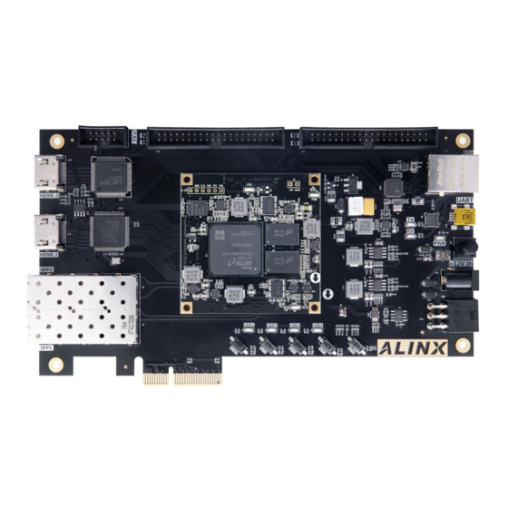
ARTIX-7 FPGA Development Board AX7A035 User Manual Part 1: FPGA Development Board Introduction The entire structure of the AX7A035 FPGA development board is inherited from our consistent core board + carrier board model. A high-speed inter-board connector is used between the core board and the carrier board. - Page 7 ARTIX-7 FPGA Development Board AX7A035 User Manual Figure 1-1-1: The Schematic Diagram of the AX7A035 Through this diagram, you can see the interfaces and functions that the AX7A035 FPGA Development Board contains: Artix-7 FPGA core board The core board consists of XC7A35T + 8Gb DDR3 + 128Mb QSPI FLASH.
- Page 8 1-port Micro SD card slot, support SD mode and SPI mode EEPROM Onboard an IIC interface EEPROM 24LC04 2-way 40-pin expansion port Reserve 2-way 40-pin 0.1inch pitch expansion port can be connected to various ALINX modules (binocular camera, TFT LCD screen, Amazon Store: https://www.amazon.com/alinx 8 / 59...
- Page 9 ARTIX-7 FPGA Development Board AX7A035 User Manual high-speed AD module, etc.). The expansion port contains 1 channel 5V power supply, 2 channel 3.3V power supply, 3 way ground, 34 IOs port. JTAG Interface A 10-pin 0.1 inch spacing standard JTAG ports for FPGA program download and debugging.
-
Page 10: Part 2: Ac7A200 Core Board
ARTIX-7 FPGA Development Board AX7A035 User Manual Part 2: AC7A035 Core Board Part 2.1: AC7A035 Core Board Introduction AC7A035 (core board model, the same below) FPGA core board, it is based on XILINX's ARTIX-7 series 100T XC7A35T-2FGG484I. It is a high-performance core board with high speed, high bandwidth and high capacity. - Page 11 ARTIX-7 FPGA Development Board AX7A035 User Manual Figure 2-1-1: AC7A035 Core Board (Front View) Figure 2-1-2: AC7A035 Core Board (Rear View) Amazon Store: https://www.amazon.com/alinx 11 / 59...
-
Page 12: Part 2.2: Fpga Chip
Xilinx's Artix-7 series. The speed grade is 2, and the temperature grade is industry grade. This model is a FGG484 package with 484 pins. Xilinx ARTIX-7 FPGA chip naming rules as below Figure 2-2-1: The Specific Chip Model Definition of ARTIX-7 Series... -
Page 13: Part 2.3: Active Differential Crystal
GTP transceiver, connected to 1.0V; V is the termination voltage MGTAVTT of the GTP transceiver, connected to 1.2V. The Artix-7 FPGA system requires that the power-up sequence be power by V , then V , then V , and finally V . - Page 14 ARTIX-7 FPGA Development Board AX7A035 User Manual model is SiT9102 -125MHz, reference clock input for GTP transceivers. Part 2.3.1: 200Mhz Active Differential clock G1 in Figure 2-3-1 is the 200M active differential crystal that provides the development board system clock source. The crystal output is connected to the BANK34 global clock pin MRCC (R4 and T4) of the FPGA.
- Page 15 ARTIX-7 FPGA Development Board AX7A035 User Manual Part 2.3.2: 125MHz Active Differential Crystal G2 in Figure 2-3-3 is the 125MHz active differential crystal, which is the reference input clock provided to the GTP module inside the FPGA. The crystal output is connected to the GTP BANK216 clock pins MGTREFCLK0P (F6) and MGTREFCLK0N (E6) of the FPGA.
-
Page 16: Part 2.4: Ddr3 Dram
ARTIX-7 FPGA Development Board AX7A035 User Manual Part 2.4: DDR3 DRAM The FPGA core board AC7A035 is equipped with two Micron 4Gbit (512MB) DDR3 chips (8Gbit in totally), model is MT41J256M16HA-125 (compatible with MT41K256M16HA-125). The DDR3 SDRAM has a maximum operating speed of 400MHz (data rate 800Mbps). - Page 17 ARTIX-7 FPGA Development Board AX7A035 User Manual Figure 2-4-2: The DDR3 on the Core Board DDR3 DRAM pin assignment: Net Name FPGA PIN Name FPGA P/N DDR3_DQS0_P IO_L3P_T0_DQS_AD5P_35 DDR3_DQS0_N IO_L3N_T0_DQS_AD5N_35 DDR3_DQS1_P IO_L9P_T1_DQS_AD7P_35 DDR3_DQS1_N IO_L9N_T1_DQS_AD7N_35 DDR3_DQS2_P IO_L15P_T2_DQS_35 DDR3_DQS2_N IO_L15N_T2_DQS_35 DDR3_DQS3_P IO_L21P_T3_DQS_35...
- Page 18 ARTIX-7 FPGA Development Board AX7A035 User Manual DDR3_DQ [12] IO_L7N_T1_AD6N_35 DDR3_DQ [13] IO_L10P_T1_AD15P_35 DDR3_DQ [14] IO_L7P_T1_AD6P_35 DDR3_DQ [15] IO_L12P_T1_MRCC_35 DDR3_DQ [16] IO_L18N_T2_35 DDR3_DQ [17] IO_L16P_T2_35 DDR3_DQ [18] IO_L14P_T2_SRCC_35 DDR3_DQ [19] IO_L17N_T2_35 DDR3_DQ [20] IO_L14N_T2_SRCC_35 DDR3_DQ [21] IO_L17P_T2_35 DDR3_DQ [22] IO_L13N_T2_MRCC_35...
-
Page 19: Part 2.5: Qspi Flash
ARTIX-7 FPGA Development Board AX7A035 User Manual DDR3_A[12] IO_L4N_T0_34 DDR3_A[13] IO_L1N_T0_34 DDR3_A[14] IO_L6N_T0_VREF_34 DDR3_BA[0] IO_L9N_T1_DQS_34 DDR3_BA[1] IO_L9P_T1_DQS_34 DDR3_BA[2] IO_L11P_T1_SRCC_34 DDR3_S0 IO_L8P_T1_34 DDR3_RAS IO_L12P_T1_MRCC_34 DDR3_CAS IO_L12N_T1_MRCC_34 DDR3_WE IO_L7P_T1_34 DDR3_ODT IO_L14N_T2_SRCC_34 DDR3_RESET IO_L15P_T2_DQS_34 DDR3_CLK_P IO_L3P_T0_DQS_34 DDR3_CLK_N IO_L3N_T0_DQS_34 DDR3_CKE IO_L14P_T2_SRCC_34 Part 2.5: QSPI Flash The FPGA core board AC7A035 is equipped with one 128Mbit QSPI FLASH, and the model is N25Q128, which uses the 3.3V CMOS voltage... - Page 20 ARTIX-7 FPGA Development Board AX7A035 User Manual Figure 2-5-1: QSPI Flash Schematic QSPI Flash pin assignments: Net Name FPGA PIN Name FPGA P/N QSPI_CLK CCLK_0 QSPI_CS IO_L6P_T0_FCS_B_14 QSPI_DQ0 IO_L1P_T0_D00_MOSI_14 QSPI_DQ1 IO_L1N_T0_D01_DIN_14 QSPI_DQ2 IO_L2P_T0_D02_14 QSPI_DQ3 IO_L2N_T0_D03_14 Figure 2-5-1: QSPI FLASH on the Core Board Amazon Store: https://www.amazon.com/alinx...
-
Page 21: Part 2.6: Led Light On Core Board
ARTIX-7 FPGA Development Board AX7A035 User Manual Part 2.6: LED Light on Core Board There are 3 red LED lights on the AC7A035 FPGA core board, one of which is the power indicator light (PWR), one is the configuration LED light (DONE), and one is the user LED light. -
Page 22: Part 2.7: Jtag Interface
ARTIX-7 FPGA Development Board AX7A035 User Manual Figure 2-6-2: LED lights on the Core Board User LEDs Pin Assignment Signal Name FPGA Pin Name FPGA Pin Number Description LED1 IO_L15N_T2_DQS_34 User LED Part 2.7: JTAG Interface The JTAG test socket J1 is reserved on the AC7A035 core board for JTAG download and debugging when the core board is used alone. -
Page 23: Part 2.8: Power Interface On The Core Board
ARTIX-7 FPGA Development Board AX7A035 User Manual GND, +3.3V these six signals. Figure 2-7-1: JTAG Interface Schematic The JTAG interface J1 on AC7A035 FPGA core board uses a 6-pin 2.54mm pitch single-row test hole. If you need to use the JTAG connector to debug on the core board, you need to solder a 6-pin single-row pin header. -
Page 24: Part 2.9: Board To Board Connectors Pin Assignment
ARTIX-7 FPGA Development Board AX7A035 User Manual Figure 2-8-2:Power interface on the Core Board Part 2.9: Board to Board Connectors pin assignment The core board has a total of four high-speed board to board connectors. The core board uses four 80-pin inter-board connectors to connect to the carrier board. - Page 25 ARTIX-7 FPGA Development Board AX7A035 User Manual PIN9 Ground PIN10 Ground PIN11 PIN12 PIN13 PIN14 PIN15 PIN16 B13_L4_P AA15 3.3V PIN17 PIN18 B13_L4_N AB15 3.3V PIN19 Ground PIN20 Ground PIN21 B13_L5_P 3.3V PIN22 B13_L1_P 3.3V PIN23 B13_L5_N AA14 3.3V PIN24...
- Page 26 ARTIX-7 FPGA Development Board AX7A035 User Manual PIN75 B16_L8_P 3.3V PIN76 PIN77 B16_L8_N 3.3V PIN78 PIN79 PIN80 The Pin1 of the connector has been marked with a dot on the board. Figure 2-9-1: Board to Board Connectors CON1 on the Core Board...
- Page 27 ARTIX-7 FPGA Development Board AX7A035 User Manual PIN27 B13_L10_N 3.3V PIN28 B14_L17_N AB18 3.3V PIN29 Ground PIN30 Ground PIN31 B13_L9_N AA11 3.3V PIN32 B14_L6_N 3.3V PIN33 B13_L9_P AA10 3.3V PIN34 B13_IO0 3.3V PIN35 B13_L8_N AB10 3.3V PIN36 B14_L7_N 3.3V PIN37 B13_L8_P 3.3V...
- Page 28 ARTIX-7 FPGA Development Board AX7A035 User Manual Board to Board Connectors CON3 The 80-pin connector CON3 is used to extend the normal IO of the BANK15 and BANK16 of the FPGA. In addition, four JTAG signals are also connected to the carrier board via the CON3 connector. The voltage standards of BANK15 and BANK16 can be adjusted by an LDO chip.
- Page 29 ARTIX-7 FPGA Development Board AX7A035 User Manual PIN45 B15_L20_P 3.3V PIN46 B15_L6_N 3.3V PIN47 B15_L20_N 3.3V PIN48 B15_L6_P 3.3V PIN49 Ground PIN50 Ground PIN51 B15_L14_P 3.3V PIN52 B15_L13_N 3.3V PIN53 B15_L14_N 3.3V PIN54 B15_L13_P 3.3V PIN55 B15_L21_P 3.3V PIN56 B15_L10_P 3.3V...
- Page 30 ARTIX-7 FPGA Development Board AX7A035 User Manual replaced by a suitable LDO. The high-speed data and clock signals of the GTP are strictly differential routed on the core board. The data lines are equal in length and kept at a certain interval to prevent signal interference.
-
Page 31: Part 2.10: Power Supply
ARTIX-7 FPGA Development Board AX7A035 User Manual PIN55 B16_L11_P 3.3V PIN56 B16_L12_P 3.3V PIN57 B16_L11_N 3.3V PIN58 B16_L12_N 3.3V PIN59 Ground PIN60 Ground PIN61 B16_L13_P 3.3V PIN62 B16_L14_P 3.3V PIN63 B16_L13_N 3.3V PIN64 B16_L14_N 3.3V PIN65 B16_L15_P 3.3V PIN66 B16_L16_P 3.3V... - Page 32 ARTIX-7 FPGA Development Board AX7A035 User Manual Figure 2-10-1:Power Supply on core board schematic The core board is powered by +5V and converted to +3.3V, +1.5V, +1.8V, +1.0V four-way power supply through three DC/DC power supply chip TLV62130RGT. The current of +1.0V can be up to 6A, and the other three output currents can be up to 3A.
- Page 33 MGTVCC(+1.0V) GTP Transceiver Bank216 of FPGA Because the power supply of Artix-7 FPGA has the power-on sequence requirement, in the circuit design, we have designed according to the power requirements of the chip, and the power-on is 1.0V->1.8V->(1.5 V, 3.3V, VCCIO) and 1.0V->...
-
Page 34: Part 2.11: Size Dimension
ARTIX-7 FPGA Development Board AX7A035 User Manual Part 2.11: Size Dimension Figure 2-11-1: AC7A035 FPGA Core board (Top view) Figure 2-11-2: AC7A035 FPGA Core board (Bottom view) Amazon Store: https://www.amazon.com/alinx 34 / 59... -
Page 35: Part 3: Carrier Board
ARTIX-7 FPGA Development Board AX7A035 User Manual Part 3: Carrier Board Part 3.1: Carrier Board Introduction Through the previous function introduction, you can understand the function of the carrier board part 1-channel PCIe x2 high speed data transmission interface ... -
Page 36: Part 3.2: Gigabit Ethernet Interface
ARTIX-7 FPGA Development Board AX7A035 User Manual Part 3.2: Gigabit Ethernet Interface The AX7A035 FPGA development board provides users with 1-channel Gigabit network communication service through the Micrel KSZ9031RNX Ethernet PHY chip. The Ethernet PHY chip is connected to the IO interface of the ARTIX7 FPGA. - Page 37 ARTIX-7 FPGA Development Board AX7A035 User Manual Figure 3-2-1: Gigabit Ethernet Interface Schematic Figure 3-3-2: Gigabit Ethernet interface on the Carrier board Gigabit Ethernet Chip PHY pin assignments are as follows: Signal Name FPGA Pin Number Description RGMII transmit clock...
-
Page 38: Part 3.3: Sfp Interface
ARTIX-7 FPGA Development Board AX7A035 User Manual Receive Data Bit1 ETH_RXD1 Receive Data Bit2 ETH_RXD2 Receive Data Bit3 ETH_RXD3 Receive data valid signal ETH_RXCTL MDIO Management Clock ETH_MDC MDIO Management Data ETH_MDIO PHY Chip Reset Signal ETH_RESET Part 3.3: SFP Interface The AX7A035 FPGA development board has two optical interfaces. - Page 39 ARTIX-7 FPGA Development Board AX7A035 User Manual Figure 3-3-2: SFP interfaces on the Carrier Board The 1 fiber interface FPGA pin assignment is as follows: Signal Name FPGA PIN Description SFP1_TX_P SFP1 Data Transfer (Positive) SFP1_TX_N SFP1 Data Transfer (Negative)
-
Page 40: Part 3.4: Pcie X2 Interface
ARTIX-7 FPGA Development Board AX7A035 User Manual Part 3.4: PCIe x2 Interface The AX7A035 FPGA development board provides an industrial-grade high-speed data transfer PCIe x2 interface. The PCIE card interface conforms to the standard PCIe card electrical specifications and can be used directly on the x2 PCIe slot of a normal PC. -
Page 41: Part 3.5: Hdmi Output Interface
ARTIX-7 FPGA Development Board AX7A035 User Manual Figure 3-4-2: PCIex2 on the Carrier Board PCIex2 Interface Pin Assignment: Signal Name FPGA Pin Description PCIE Channel 0 Data Receive Positive PCIE_RX0_P PCIE Channel 0 Data Receive Negative PCIE_RX0_N PCIE Channel 1 Data Receive Positive... - Page 42 ARTIX-7 FPGA Development Board AX7A035 User Manual Figure 3-5-1: HDMI Output Schematic Figure 3-5-1: HDMI Output on the Carrire Board HDMI Input Pin Assignment: Signal Name FPGA Pin 9134_NRESET 9134_CLK 9134_HS 9134_VS 9134_DE 9134_D[0] 9134_D[1] 9134_D[2] 9134_D[3] 9134_D[4] Amazon Store: https://www.amazon.com/alinx...
-
Page 43: Part 3.6: Hdmi Input Interface
ARTIX-7 FPGA Development Board AX7A035 User Manual 9134_D[5] 9134_D[6] 9134_D[7] 9134_D[8] 9134_D[9] 9134_D[10] 9134_D[11] AB18 9134_D[12] AA18 9134_D[13] AA19 9134_D[14] AB20 9134_D[15] AA20 9134_D[16] AA21 9134_D[17] AB22 9134_D[18] AB21 9134_D[19] 9134_D[20] 9134_D[21] 9134_D[22] 9134_D[23] HDMI_SCL HDMI_SDA Part 3.6: HDMI Input interface... - Page 44 ARTIX-7 FPGA Development Board AX7A035 User Manual Figure 3-6-1: HDMI Input Schematic Figure 3-6-2: HDMI Input on the Carrier Board HDMI Input Pin Assignment: Signal Name FPG Pin Number 9013_NRESET 9013_CLK 9013_HS 9013_VS 9013_DE 9013_D[0] 9013_D[1] 9013_D[2] 9013_D[3] Amazon Store: https://www.amazon.com/alinx...
-
Page 45: Part 3.7: Sd Card Slot
ARTIX-7 FPGA Development Board AX7A035 User Manual 9013_D[4] 9013_D[5] 9013_D[6] 9013_D[7] 9013_D[8] 9013_D[9] 9013_D[10] 9013_D[11] 9013_D[12] 9013_D[13] 9013_D[14] 9013_D[15] 9013_D[16] 9013_D[17] 9013_D[18] 9013_D[19] 9013_D[20] 9013_D[21] 9013_D[22] 9013_D[23] HDMI_SCL HDMI_SDA Part 3.7: SD Card Slot The SD card (Secure Digital Memory Card) is a memory card based on the semiconductor flash memory process. - Page 46 ARTIX-7 FPGA Development Board AX7A035 User Manual include IBM, Microsoft, Motorola, NEC, Samsung, and others. Driven by these leading manufacturers, SD cards have become the most widely used memory card in consumer digital devices. The SD card is a very common storage device. The extended SD card supports SPI mode and SD mode.
-
Page 47: Part 3.8: Usb-To-Uart Bridge Connector
ARTIX-7 FPGA Development Board AX7A035 User Manual Part 3.8: USB-to-Uart Bridge Connector The AX7A035 FPGA development board includes the USB-UAR chip of Silicon Labs CP2102GM. The USB interface uses the MINI USB interface. It can be connected to the USB port of the upper PC for serial data communication with a USB cable. -
Page 48: Part 3.9: Eeprom 24Lc04
ARTIX-7 FPGA Development Board AX7A035 User Manual Figure 3-8-3: Serial Port communication LED Indicators Schematic USB-to-UART pin assignment: Signal Name FPGA PIN UART1_RXD UART1_TXD Part 3.9: EEPROM 24LC04 AX7A035 carrier board contains an EEPROM, model 24LC04, and has a capacity of 4Kbit (2*256*8bit). It consists of two 256-byte blocks and communicates via the IIC bus. -
Page 49: Part 3.10: Temperature Sensor
ARTIX-7 FPGA Development Board AX7A035 User Manual Figure 3-9-2: EEPROM on the Carrier Board EEPROM Pin Assignment Net Name FPGA PIN I2C_SCL I2C_SDA Part 3.10: Temperature Sensor A high-precision, low-power, digital temperature sensor chip is mounted on the AX7A035 FPGA development board, and the model is LM75 of ON Semiconductor. -
Page 50: Part 3.11: Expansion Header
Part 3.11: Expansion Header The carrier board is reserved with two 0.1inch spacing standard 40-pin expansion ports J11 and J13, which are used to connect the ALINX modules or the external circuit designed by the user. The expansion port has 40 signals, of which 1-channel 5V power supply, 2-channel 3.3 V power supply, 3-channle... - Page 51 ARTIX-7 FPGA Development Board AX7A035 User Manual Figure 3-11-1: Expansion header J11 schematic The figure 3-11-2 detailed the J11 expansion port on the carrier board. The Pin1 and Pin2 of the expansion port are already marked on the board. Figure 3-11-2: Expansion header J11 on the Carrier Board...
- Page 52 ARTIX-7 FPGA Development Board AX7A035 User Manual +3.3V +3.3V Figure 3-11-3: Expansion header J13 schematic Amazon Store: https://www.amazon.com/alinx 52 / 59...
- Page 53 ARTIX-7 FPGA Development Board AX7A035 User Manual The figure 3-11-4 detailed the J13 expansion port on the carrier board. The Pin1 and Pin2 of the expansion port are already marked on the board. Figure 3-11-4: Expansion header J13 on the carrier board...
-
Page 54: Part 3.12: Jtag Interface
ARTIX-7 FPGA Development Board AX7A035 User Manual Part 3.12: JTAG Interface The development board reserves a JTAG interface for downloading FPGA programs or firmware to FLASH. In order to prevent damage to the FPGA chip caused by hot plugging, we added a protection diode to the JTAG signal to ensure that the signal voltage is within the range accepted by the FPGA to avoid damage to the FPGA. - Page 55 ARTIX-7 FPGA Development Board AX7A035 User Manual The key is active low. When the key is pressed, the IO input voltage of the FPGA is low. When no key is pressed, The IO input voltage of the FPGA is high.
-
Page 56: Part 3.14: Led Light
ARTIX-7 FPGA Development Board AX7A035 User Manual Part 3.14: LED Light There are 7 red LEDs on the AX7A035 FPGA carrier board, one of which is the power indicator (PWR), two are USB Uart data receiving and transmitting indicators, and four are users LED lights (LED1~LED4). When the board is powered on, the power indicator will light up;... -
Page 57: Part 3.15: Power Supply
ARTIX-7 FPGA Development Board AX7A035 User Manual Part 3.15: Power Supply The power input voltage of the AX7A035 FPGA development board is DC12V. The development board also supports power from the PCIe interface. At the same time, it supports direct power from the ATX chassis power supply (12V). -
Page 58: Part 3.16: Fan
ARTIX-7 FPGA Development Board AX7A035 User Manual Figure 3-15-3: Power Supply Circuit on the Carrier Board Part 3.16: Fan Because the FPGA chip generates a lot of heat when it works normally, we add a heat sink and fan to the chip to prevent the chip from overheating. The fan is controlled by the FPGA chip. -
Page 59: Part 3.17: Carrier Board Size Dimension
ARTIX-7 FPGA Development Board AX7A035 User Manual The fan has been screwed to the development board before leaving the factory. The power of the fan is connected to the J8 socket. The red is positive and the black is negative.
Need help?
Do you have a question about the ARTIX-7 FPGA and is the answer not in the manual?
Questions and answers