Table of Contents
Advertisement
Quick Links
Advertisement
Table of Contents

Related Manuals for Alinx AX7102


Summary of Contents for Alinx AX7102
- Page 1 ARTIX-7 FPGA Development Board AX7102 User Manual...
-
Page 2: Version Record
2020-10-28 Rachel Zhou First Release The English version was translated by Shanghai Tianhui Trading Company. They has not been officially Review by ALINX and are for reference only. If there are any errors, please send email to rachel.zhou@aithtech.com for correction. -
Page 3: Table Of Contents
ARTIX-7 FPGA Development Board AX7102 User Manual Table of Contents Version Record .....................2 Part 1: FPGA Development Board Introduction .......... 6 Part 2: AC7100B core board ..............10 Part 2.1: AC7100B Core Board Introduction ........10 Part 2.2: FPGA Chip ................12 Part 2.3: Active Differential Crystal .............13... - Page 4 ARTIX-7 FPGA Development Board AX7102 User Manual Part 3.12: JTAG Interface ..............52 Part 3.13: keys ..................53 Part 3.14: LED Light ................54 Part 3.15: Power Supply ..............55 Amazon Store: https://www.amazon.com/alinx 4 / 57 Sales Email: rachel.zhou@aithtech.com...
- Page 5 ARTIX-7 FPGA Development Board AX7102 User Manual This ARTIX-7 FPGA development platform adopts the core board + carrier board mode, which is convenient for users to use the core board for secondary development. In the design of carrier board, we have extended a wealth of interfaces for users, such as 2 fiber interfaces, 1 Gigabit Ethernet interfaces, 1 USB2.0 , VGT...
-
Page 6: Part 1: Fpga Development Board Introduction
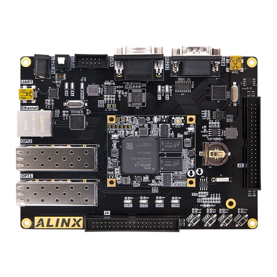
ARTIX-7 FPGA Development Board AX7102 User Manual Part 1: FPGA Development Board Introduction The entire structure of the AX7102 FPGA development board is inherited from our consistent core board + carrier board model. A high-speed inter-board connector is used between the core board and the carrier board. - Page 7 ARTIX-7 FPGA Development Board AX7102 User Manual Figure 1-1-1: The Schematic Diagram of the AX7102 Through this diagram, you can see the interfaces and functions that the AX7102 FPGA Development Board contains: Artix-7 FPGA core board The core board consists of XC7A100T + 8Gb DDR3 + 128Mb QSPI FLASH.
- Page 8 ARTIX-7 FPGA Development Board AX7102 User Manual RTL8211EG chip supports 10/100/1000 Mbps network transmission rate. Full duplex and adaptive 2-channel high-speed SFP Interface The two high-speed transceivers of the GTP transceiver of ARTIX-7 FPGA are connected to the transmission and reception of two optical modules to realize two high-speed optical fiber communication interfaces.
- Page 9 ARTIX-7 FPGA Development Board AX7102 User Manual Onboard an IIC interface EEPROM 24LC04 2-way 40-pin expansion port 2-way 40-pin 0.1inch spacing expansion port can be connected to various ALINX modules (binocular camera, TFT LCD screen, high-speed AD module, etc.). The expansion port contains 1 channel 5V power supply, 2 channel 3.3V power supply, 3 way ground, 34 IOs...
-
Page 10: Part 2: Ac7100B Core Board
ARTIX-7 FPGA Development Board AX7102 User Manual Part 2: AC7100B core board Part 2.1: AC7100B Core Board Introduction AC7100B (core board model, the same below) FPGA core board, it is based on XILINX's ARTIX-7 series 100T XC7A100T-2FGG484I. It is a high-performance core board with high speed, high bandwidth and high capacity. - Page 11 ARTIX-7 FPGA Development Board AX7102 User Manual Figure 2-1-1: AC7100B Core Board (Front View) Figure 2-1-2: AC7100B Core Board (Rear View) Amazon Store: https://www.amazon.com/alinx 11 / 57 Sales Email: rachel.zhou@aithtech.com...
-
Page 12: Part 2.2: Fpga Chip
ARTIX-7 FPGA Development Board AX7102 User Manual Part 2.2: FPGA Chip As mentioned above, the FPGA model we use is XC7A100T-2FGG484I, which belongs to Xilinx's Artix-7 series. The speed grade is 2, and the temperature grade is industry grade. This model is a FGG484 package with 484 pins. -
Page 13: Part 2.3: Active Differential Crystal
ARTIX-7 FPGA Development Board AX7102 User Manual FPGA power supply system Artix-7 FPGA power supplies are V CCINT CCBRAM CCAUX MGTAVCC is the FPGA core power supply pin, which needs to be connected MGTAVTT CCINT to 1.0V; V is the power supply pin of FPGA block RAM, connect to 1.0V;... - Page 14 ARTIX-7 FPGA Development Board AX7102 User Manual BANK34 global clock pin MRCC (R4 and T4) of the FPGA. This 200Mhz differential clock can be used to drive the user logic in the FPGA. Users can configure the PLLs and DCMs inside the FPGA to generate clocks of different frequencies.
- Page 15 ARTIX-7 FPGA Development Board AX7102 User Manual output is connected to the GTP BANK216 clock pins MGTREFCLK0P (F6) and MGTREFCLK0N (E6) of the FPGA. Figure 2-3-3: 125Mhz Active Differential Crystal Schematic Figure 2-3-4: 125Mhz Active Differential Crystal on the Core Board...
-
Page 16: Part 2.4: Ddr3 Dram
ARTIX-7 FPGA Development Board AX7102 User Manual Part 2.4: DDR3 DRAM The FPGA core board AC7100B is equipped with two Micron 4Gbit (512MB) DDR3 chips, model MT41J256M16HA-125 (compatible with MT41K256M16HA-125). The DDR3 SDRAM has a maximum operating speed of 800MHz (data rate 1600Mbps). The DDR3 memory system is directly connected to the memory interface of the BANK 34 and BANK35 of the FPGA. - Page 17 ARTIX-7 FPGA Development Board AX7102 User Manual Figure 2-4-2: The DDR3 on the Core Board DDR3 DRAM pin assignment: Net Name FPGA PIN Name FPGA P/N DDR3_DQS0_P IO_L3P_T0_DQS_AD5P_35 DDR3_DQS0_N IO_L3N_T0_DQS_AD5N_35 DDR3_DQS1_P IO_L9P_T1_DQS_AD7P_35 DDR3_DQS1_N IO_L9N_T1_DQS_AD7N_35 DDR3_DQS2_P IO_L15P_T2_DQS_35 DDR3_DQS2_N IO_L15N_T2_DQS_35 DDR3_DQS3_P IO_L21P_T3_DQS_35...
-
Page 18: Part 2.5: Qspi Flash
ARTIX-7 FPGA Development Board AX7102 User Manual DDR3_DQ [4] IO_L2N_T0_AD12N_35 DDR3_DQ [5] IO_L5N_T0_AD13N_35 DDR3_DQ [6] IO_L1P_T0_AD4P_35 DDR3_DQ [7] IO_L4P_T0_35 DDR3_DQ [8] IO_L11P_T1_SRCC_35 DDR3_DQ [9] IO_L11N_T1_SRCC_35 DDR3_DQ [10] IO_L8P_T1_AD14P_35 DDR3_DQ [11] IO_L10N_T1_AD15N_35 DDR3_DQ [12] IO_L7N_T1_AD6N_35 DDR3_DQ [13] IO_L10P_T1_AD15P_35 DDR3_DQ [14] IO_L7P_T1_AD6P_35... - Page 19 ARTIX-7 FPGA Development Board AX7102 User Manual the FPGA chip. The clock pin is connected to CCLK0 of BANK0, and other data and chip select signals are connected to D00~D03 and FCS pins of BANK14 respectively. Figure 2-5-1 shows the hardware connection of QSPI Flash.
-
Page 20: Part 2.6: Led Light On Core Board
ARTIX-7 FPGA Development Board AX7102 User Manual Part 2.6: LED Light on Core Board There are 3 red LED lights on the AC7100B FPGA core board, one of which is the power indicator light (PWR), one is the configuration LED light (DONE), and one is the user LED light. -
Page 21: Part 2.8: Jtag Interface
ARTIX-7 FPGA Development Board AX7102 User Manual the reset key connection is shown in Figure 2-7-1: Figure 2-7-1: Reset key Schematic Figure 2-7-2: Reset key on the Core Board Reset key pin assignment Signal Name ZYNQ Pin Name ZYNQ Pin Number... -
Page 22: Part 2.9: Power Interface On The Core Board
ARTIX-7 FPGA Development Board AX7102 User Manual The JTAG interface J1 on AC7100B FPGA core board uses a 6-pin 2.54mm pitch single-row test hole. If you need to use the JTAG connection to debug on the core board, you need to solder a 6-pin single-row pin header. -
Page 23: Part 2.10: Board To Board Connectors Pin Assignment
ARTIX-7 FPGA Development Board AX7102 User Manual Figure 2-9-2:J3 interface on the Core Board Part 2.10: Board to Board Connectors pin assignment The core board has a total of four high-speed board to board connectors. The core board uses four 80-pin inter-board connectors to connect to the carrier board. - Page 24 ARTIX-7 FPGA Development Board AX7102 User Manual Pin Assignment of Board to Board Connectors CON1 CON1 Signal Name FPGA Pin Voltage CON1 Signal Name FPGA Pin Voltage Level Level PIN1 VCCIN PIN2 VCCIN PIN3 VCCIN PIN4 VCCIN PIN5 VCCIN PIN6...
- Page 25 ARTIX-7 FPGA Development Board AX7102 User Manual PIN59 Ground PIN60 Ground PIN61 B16_L1_N 3.3V PIN62 PIN63 B16_L1_P 3.3V PIN64 PIN65 B16_L4_N 3.3V PIN66 PIN67 B16_L4_P 3.3V PIN68 PIN69 Ground PIN70 Ground PIN71 B16_L6_N 3.3V PIN72 Board to Board Connectors CON2 The 80-pin female connection header CON2 is used to extend the normal IO of the BANK13 and BANK14 of the FPGA.
- Page 26 ARTIX-7 FPGA Development Board AX7102 User Manual PIN33 B13_L9_P AA10 3.3V PIN34 B13_IO0 3.3V PIN35 B13_L8_N AB10 3.3V PIN36 B14_L7_N 3.3V PIN37 B13_L8_P 3.3V PIN38 B14_L7_P 3.3V PIN39 Ground PIN40 Ground PIN41 B14_L11_N 3.3V PIN42 B14_L4_P 3.3V PIN43 B14_L11_P 3.3V...
- Page 27 ARTIX-7 FPGA Development Board AX7102 User Manual a suitable LDO. Pin Assignment of Board to Board Connectors CON3 CON1 Signal Name FPGA CON1 Signal Name FPGA Pin Voltage Voltage Level Level PIN1 B15_IO0 3.3V PIN2 B15_IO25 3.3V PIN3 B16_IO0 3.3V...
- Page 28 ARTIX-7 FPGA Development Board AX7102 User Manual PIN57 B15_L21_N 3.3V PIN58 B15_L10_N 3.3V PIN59 Ground PIN60 Ground PIN61 B15_L23_P 3.3V PIN62 B15_L18_P 3.3V PIN63 B15_L23_N 3.3V PIN64 B15_L18_N 3.3V PIN65 B15_L22_P 3.3V PIN66 B15_L17_N 3.3V PIN67 B15_L22_N 3.3V PIN68 B15_L17_P 3.3V...
- Page 29 ARTIX-7 FPGA Development Board AX7102 User Manual PIN15 Ground PIN16 Ground PIN17 MGT_TX3_P Differential PIN18 MGT_RX2_P Differential PIN19 MGT_TX3_N Differential PIN20 MGT_RX2_N Differential PIN21 Ground PIN22 Ground PIN23 MGT_RX3_P Differential PIN24 MGT_TX0_P Differential PIN25 MGT_RX3_N Differential PIN26 MGT_TX0_N Differential PIN27...
-
Page 30: Part 2.11: Power Supply
ARTIX-7 FPGA Development Board AX7102 User Manual PIN79 PIN80 Part 2.11: Power Supply The AC7100B FPGA core board is powered by DC5V via carrier board, and it is powered by the J3 interface when it is used alone. Please be careful not to supply power to J3 interface and the carrier board at the same time to avoid damage. - Page 31 ARTIX-7 FPGA Development Board AX7102 User Manual following table: Power Supply Function +1.0V FPGA Core Voltage +1.8V FPGA auxiliary voltage, TPS74801 power supply +3.3V VCCIO of Bank0,Bank13 and Bank14 of FPGA,QSIP FLASH, Clock Crystal +1.5V DDR3, Bank34 and Bank35 of FPGA VREF,VTT(+0.75V)
-
Page 32: Part 2.12: Form Factors
ARTIX-7 FPGA Development Board AX7102 User Manual Part 2.12: Form Factors Figure 2-12-1: AC7100B FPGA Core board (Top view) Figure 2-12-2: AC7100B FPGA Core board (Bottom view) Amazon Store: https://www.amazon.com/alinx 32 / 57 Sales Email: rachel.zhou@aithtech.com... -
Page 33: Part 3: Carrier Board
ARTIX-7 FPGA Development Board AX7102 User Manual Part 3: Carrier Board Part 3.1: Carrier Board Introduction Through the previous function introduction, you can understand the function of the carrier board part 1-channel 10/100M/1000M Ethernet RJ-45 interface 2-channel SFP interface ... -
Page 34: Part 3.2: Gigabit Ethernet Interface
4 independent keys 4 user LED lights Part 3.2: Gigabit Ethernet Interface The AX7102 carrier board provides users with one-channel Gigabit network communication service through the Realtek RTL8211EG Ethernet PHY chip. The RTL8211EG chip supports 10/100/1000 Mbps network transmission rate and communicates with the FPGA through the GMII interface. - Page 35 ARTIX-7 FPGA Development Board AX7102 User Manual FPGA and PHY chip RTL8211EG is communicated through the GMII bus, the transmission clock is 25Mhz. The receive clock E_RXC is provided by the PHY chip, the transmit clock E_GTXC is provided by the FPGA, and the data is sampled on the rising edge of the clock.
-
Page 36: Part 3.3: Sfp Interface
Ethernet MDIO Management Data Part 3.3: SFP Interface The AX7102 Carrier board has two optical interfaces. Users can purchase SFP optical modules (1.25G, 2.5G optical modules on the market) and insert them into these two optical interfaces for optical data communication. The two fiber interfaces are connected to the two RX/TX of the GNK transceiver of the FPGA. - Page 37 ARTIX-7 FPGA Development Board AX7102 User Manual clock for the GTX transceiver is provided by the 125M differential clock of AC7100 FPGA core board. Figure 3-3-1 detailed the schematic diagram of FPGA and fiber design Figure 3-3-1: SFP Interface Schematic...
-
Page 38: Part 3.4: Vga Display Interface
10-bit D/A converters. It converts the input RGB digital signals into VGA video signals, and supports up to 1080p@60Hz output. In the AX7102 carrier board, the RGB digital signal output by the FPGA is 24-bit color, and the red, green and blue colors are 8 bits each. In the... - Page 39 ARTIX-7 FPGA Development Board AX7102 User Manual Figure 3-4-1: VGA Display Interface Schematic Figure 3-4-2: VGA Display Interface on the Carrier Board VGA Pin Assignment: Signal Name FPGA Pin VGA_CLK VGA_EN AB20 VGA_HS AA11 VGA_VS AA10 VGA_R7 VGA_R6 VGA_R5 Amazon Store: https://www.amazon.com/alinx...
-
Page 40: Part 3.5: Usb2.0 Interface
VGA_B0 AA19 Part 3.5: USB2.0 Interface The AX7102 carrier board uses Cypress CY7C68013A USB2.0 controller chip to realize high-speed data communication between PC and FPGA. CY7C68013A controller fully complies with the universal serial bus protocol version 2.0 specifications, supports full speed (12Mbit/s) and low speed (1.5Mbit/s) mode. - Page 41 ARTIX-7 FPGA Development Board AX7102 User Manual communication between CY7C68013A and other devices is very simple. It provides GPIF and FIFO modes for seamless data exchange with FPGA, DSP, ATA, UTOPIA, EPP, PCMCIA and so on. The clock of the CY7C68013A transceiver is provided by a 24MHz crystal.
-
Page 42: Part 3.6: Sd Card Slot
ARTIX-7 FPGA Development Board AX7102 User Manual USB 2.0 Pin Assignment Signal Name FPGA PIN Description USB_CLKOUT 12, 24 or 48 MHz Clock Output USB_IFCLK Synchronous communication clock signal USB_FLAGA Programmable slave-FIFO output status flag signal USB_FLAGB Programmable slave-FIFO output status flag signal... - Page 43 ARTIX-7 FPGA Development Board AX7102 User Manual based on the semiconductor flash memory process. It was completed in 1999 by the Japanese Panasonic-led concept, and the participants Toshiba and SanDisk of the United States conducted substantial research and development. In 2000, these companies launched the SD Association (Secure Digital Association), which has a strong lineup and attracted a large number of vendors.
-
Page 44: Part 3.7: Usb To Serial Port
ARTIX-7 FPGA Development Board AX7102 User Manual SD card slot pin assignment: SD Mode Signal Name FPGA PIN SD_CLK SD_CMD SD_CD_N SD_DAT0 SD_DAT1 SD_DAT2 SD_DAT3 Part 3.7: USB to Serial Port The development board includes the USB-UAR chip of Silicon Labs CP2102GM. - Page 45 ARTIX-7 FPGA Development Board AX7102 User Manual Figure 3-7-2: USB to serial port on the Carrier Board At the same time, two LED indicators (LED7 and LED8) are set for the serial port signal, and the silkscreen on the PCB is TX and RX, indicating that...
-
Page 46: Part 3.8: Rs232 Interface
ARTIX-7 FPGA Development Board AX7102 User Manual Part 3.8: RS232 Interface The AX7102 carrier board contains an RS232 male socket. Using the MAX3232 chip as a bridge for RS232 and UART level shifting, users need to prepare an RS232 serial cable (straight cable) to connect the development board to a PC or other peripheral for RS232 serial data communication. -
Page 47: Part 3.9: Eeprom 24Lc04
ARTIX-7 FPGA Development Board AX7102 User Manual Part 3.9: EEPROM 24LC04 AX7102 carrier board contains an EEPROM, model 24LC04, and has a capacity of 4Kbit (2*256*8bit). It consists of two 256-byte blocks and communicates via the IIC bus. The onboard EEPROM is to learn how to communicate with the IIC bus. -
Page 48: Part 3.10: Real Time Clock Ds1302
ARTIX-7 FPGA Development Board AX7102 User Manual Part 3.10: Real time clock DS1302 The AX7102 carrier board contains a real-time clock RTC chip, model DS1302, which provides a calendar function up to 2099, with days, minutes, minutes, seconds and weeks. If time is needed in the system, then the RTC needs to be involved in the product. -
Page 49: Part 3.11: Expansion Header
Part 3.11: Expansion Header The carrier board is reserved with two 2.54-mm standard 40-pin expansion ports J4 and J5, which are used to connect the ALINX modules or the external circuit designed by the user. The expansion port has 40 signals, of which 1-channel 5V power supply, 2-channel 3.3 V power supply, 3-channle ground... - Page 50 ARTIX-7 FPGA Development Board AX7102 User Manual circuit of the expansion port (J4) is shown in Figure 3-11-1. Figure 3-11-1: Expansion header J4 schematic Figure 3-11-2: Expansion header J4 on the Carrier Board J4 Expansion Header Pin Assignment J4 Pin Number...
- Page 51 ARTIX-7 FPGA Development Board AX7102 User Manual +3.3V +3.3V Figure 3-11-3: Expansion header J5 schematic Figure 3-11-4: Expansion header J5 on the Carrier Board Amazon Store: https://www.amazon.com/alinx 51 / 57 Sales Email: rachel.zhou@aithtech.com...
-
Page 52: Part 3.12: Jtag Interface
+3.3V Part 3.12: JTAG Interface A JTAG interface is reserved on the AX7102 FPGA carrier board for downloading FPGA programs or firmware to FLASH. In order to prevent damage to the FPGA chip caused by hot plugging, a protection diode is added to the JTAG signal to ensure that the voltage of the signal is within the range accepted by the FPGA to avoid damage of the FPGA chip. -
Page 53: Part 3.13: Keys
Be careful not to hot swap when JTAG cable is plugged and unplugged. Part 3.13: keys The AX7102 FPGA carrier board contains four user keys KEY1~KEY4. All keys are connected to the normal IO of the FPGA. The key is active low. When the key is pressed, the IO input voltage of the FPGA is low. -
Page 54: Part 3.14: Led Light
KEY4 Part 3.14: LED Light There are nine red LEDs on the AX7102 FPGA carrier board, one of which is the power indicator (PWR), two are USB Uart data receiving and transmitting indicators, two are RS232 data receiving and transmitting indicators, and four are users LED lights (LED1~LED4). -
Page 55: Part 3.15: Power Supply
LED4 Part 3.15: Power Supply The power input voltage of the AX7102 FPGA development board is DC12V. The carrier board is converted into +5V and +3.3V two-way power supply through one DC/DC power supply chip. In addition, the +5V power... - Page 56 ARTIX-7 FPGA Development Board AX7102 User Manual inter-board connector. The power supply design on the expansion is shown in Figure 3-15-1. Because the +5V power supply supplies power to the AC7Z035 FPGA core board through the inter-board connector, the DCDC power supply has a...
- Page 57 ARTIX-7 FPGA Development Board AX7102 User Manual Figure 3-15-2: +3.3V Power circuit on the Carrier Board Figure 3-15-3: +5V Power circuit on the Carrier Board Amazon Store: https://www.amazon.com/alinx 57 / 57 Sales Email: rachel.zhou@aithtech.com...
Need help?
Do you have a question about the AX7102 and is the answer not in the manual?
Questions and answers