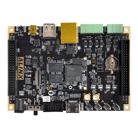
ZYNQ FPGA Development Board AX7350B User Manual Version Record Revision Date Release By Description Rev 1.0 2019-04-05 Rachel Zhou First Release 2 / 46 Amazon Store: https://www.amazon.com/alinx...
Part 16: Reset Button and User Button ..........41 Part17: JTAG Debug Port ............... 42 Part 18: DIP Switch Configuration ............43 Part 19: Power Supply ................43 Part 20: Fan ................... 45 Part 21: Dimensional structure ............... 46 3 / 46 Amazon Store: https://www.amazon.com/alinx...
Page 4
ZYNQ FPGA Development Board AX7350B User Manual The ZYNQ7000 FPGA development platform uses XILINX's Zynq7000 SOC chip XC7Z035 solution, which uses ARM+FPGA SOC technology to integrate dual-core ARM Cortex-A9 and FPGA programmable logic on a single chip. ZYNQ has two 512MB high-speed DDR3 SDRAM chips on the PS and PL sides.
USB2.0 HOST interfaces, one HDMI output interface, and one UART serial interface. 1 SD card interface, 1 FMC expansion interface and some button LEDs. Figure 1-1 is the Schematic diagram of the entire FPGA development boards: 5 / 46 Amazon Store: https://www.amazon.com/alinx...
Page 6
ZYNQ chip data, or as a memory for the operating system. The other two are attached to the PL end and can be used as data storage, image analysis cache, and data processing of the FPGA. eMMC 6 / 46 Amazon Store: https://www.amazon.com/alinx...
Page 7
ANALOG DEVICE, up to 1080P@60Hz output, support 3D output. USB2.0 HOST Interface Extend the 4-channe USB HOST interface through the USB Hub chip for connecting external USB slave devices, such as connecting a 7 / 46 Amazon Store: https://www.amazon.com/alinx...
Page 8
GTX. Provide a reference clock for PCIE, SFP and DDR operation. LED Light 9 LEDs, 1 power indicator; 1 DONE configuration indicator; 2 serial 8 / 46 Amazon Store: https://www.amazon.com/alinx...
UART interface, GPIO etc. The PS can operate independently and start up at power up or reset. Figure 2-1 detailed the Overall Block Diagram of the ZYNQ7000 Chip. Figure 2-1: Overall Block Diagram of the ZYNQ7000 Chip 9 / 46 Amazon Store: https://www.amazon.com/alinx...
Page 10
8-channel high-speed GTX transceiver, supporting PCIE Gen2x8; Two AD converters for on-chip voltage, temperature sensing and up to 17 external differential input channels, 1MBPS XC7Z020-2CLG484I chip speed grade is -2, industrial grade, package is 10 / 46 Amazon Store: https://www.amazon.com/alinx...
Page 11
FGG676, pin pitch is 1.0mm the specific chip model definition of ZYNQ7000 series is shown in Figure 2-2 Figure 2-2: The Specific Chip Model Definition of ZYNQ7000 Series Figure 2-3: The XC7Z035 chip used on the Core Board 11 / 46 Amazon Store: https://www.amazon.com/alinx...
The hardware design of DDR3 requires strict consideration of signal integrity. We have fully considered the matching resistor/terminal resistance, trace impedance control, and trace length control in circuit design and PCB design to ensure high-speed and stable operation of DDR3. 12 / 46 Amazon Store: https://www.amazon.com/alinx...
Page 13
Figure 3-2: The Schematic Part of DDR3 DRAM on the PL side PS side DDR3 DRAM pin assignment: Signal Name ZYNQ Pin Name ZYNQ Pin Number PS_DDR3_DQS0_P PS_DDR_DQS_P0_502 PS_DDR3_DQS0_N PS_DDR_DQS_N0_502 PS_DDR3_DQS1_P PS_DDR_DQS_P1_502 PS_DDR3_DQS1_N PS_DDR_DQS_N1_502 PS_DDR3_DQS2_P PS_DDR_DQS_P2_502 PS_DDR3_DQS2_N PS_DDR_DQS_N2_502 13 / 46 Amazon Store: https://www.amazon.com/alinx...
PS ports need to be configured as the QSPI FLASH interface. Figure 4-1 shows the QSPI Flash in the schematic. QSPI_CS QSPI_SCK QSPI FLASH ZYNQ BANK (W25Q256F) QSPI_D0~QSPI_D3 Figure 4-1: QSPI Flash in the schematic 18 / 46 Amazon Store: https://www.amazon.com/alinx...
ZYNQ chip. In the system design, the GPIO port functions of these PS ports need to be configured as the SD interface. Figure 5-1 shows the eMMC Flash in the schematic. 19 / 46 Amazon Store: https://www.amazon.com/alinx...
The ZYNQ chip provides a 33.333MHz clock input to the PS section via the X4 crystal on the development board. The input of the clock is connected to the pin of the PS_CLK_500 of the BANK500 of the ZYNQ chip. The schematic 20 / 46 Amazon Store: https://www.amazon.com/alinx...
Page 21
(MRCC) of the FPGA BANK35, which can be used to drive user logic circuit within the FPGA. The schematic diagram of the clock source is shown in Figure 6-2. Figure 6-2: PL system clock source 21 / 46 Amazon Store: https://www.amazon.com/alinx...
Page 22
Signal Name ZYNQ Pin CLK_50MHZ DDR Reference Clock A 200MHz differential crystal oscillator is provided to bank34 as the reference clock of the DDR controller of PL; Figure 6-3 200Mhz active crystal oscillator for DDR 22 / 46 Amazon Store: https://www.amazon.com/alinx...
Page 23
SFP_CLK0_P/N 156.25M BANK ZYNQ PCIE_CLK0_P/N BANK CLK0+ CLK0- CLOCK DSC557-0334FI1 CLK1+ CLK1- PCIE PCIE_REFCLK_P/N 插槽 Figure 6-4 Programmable clock source Programmable clock source ZYNQ pin assignment:: Signal Name ZYNQ 23 / 46 Amazon Store: https://www.amazon.com/alinx...
REGIN UART_RXD (CP2102-GM) D+/- Micro USB Figure 7-1: USB to serial port schematic USB to serial port ZYNQ pin assignment: Signal name ZYNQ Pin Name ZYNQ Pin Description Number UART_RXD PS_MIO13_500 Uart data input 24 / 46 Amazon Store: https://www.amazon.com/alinx...
Page 26
Ethernet PHY chip on the ZYNQ PL side: U169 PHY1_TXCK PHY1_TXCTL PHY1_TXD0~PHY1_TXD3 PHY1_RXCK ZYNQ BANK GPHY PHY1_RXCTL (JL2121) PHY1_TXD0~PHY1_RXD3 PHY1_MDC PHY1_MDIO PHY1_RESET BANK Figure 8-1: The connection of the ZYNQ PS end and GPHY chip 26 / 46 Amazon Store: https://www.amazon.com/alinx...
Page 27
Receive data Bit0 PHY1_RXD1 PS_MIO24_501 Receive data Bit1 PHY1_RXD2 PS_MIO25_501 Receive data Bit2 PHY1_RXD3 PS_MIO26_501 Receive data Bit3 PHY1_RXCTL PS_MIO27_501 Receive data valid signal PHY1_MDC PS_MIO52_501 MDIO Management clock PHY1_MDIO PS_MIO53_501 MDIO Management data 27 / 46 Amazon Store: https://www.amazon.com/alinx...
PS side of the ZYNQ chip. The USB interface differential signal (DP/DM) is connected to the USB2514 chip to extend the four USB ports. Two 24MHz crystals provide clocks for the USB3320C and USB2514 chips, respectively. 28 / 46 Amazon Store: https://www.amazon.com/alinx...
Page 29
PS_MIO33_501 USB Data Bit1 OTG_DATA2 PS_MIO34_501 USB Data Bit2 OTG_DATA3 PS_MIO35_501 USB Data Bit3 OTG_CLK PS_MIO36_501 USB Clock Signal OTG_DATA5 PS_MIO37_501 USB Data Bit5 OTG_DATA6 PS_MIO38_501 USB Data Bit6 OTG_DATA7 PS_MIO39_501 USB Data Bit7 29 / 46 Amazon Store: https://www.amazon.com/alinx...
Contr HDMI_SCL HDMI_SDA Figure 10-1: HDMI interface design schematic ZYNQ Pin Assignment Signal Name ZYNQ Pin Name ZYNQ Pin Description Number HDMI_CLK IO_L8P_T1_AD10P_35 HDMI Video signal clock HDMI_HSYNC IO_L23P_T3_35 HDMI Video signal line synchronization 30 / 46 Amazon Store: https://www.amazon.com/alinx...
HDMI Audio S/PDIF Output HDMI_INT IO_L15P_T2_DQS_AD12P_35 HDMI Interrupt signal HDMI_SCL IO_L18N_T2_AD13N_35 HDMI IIC Control clock HDMI _SDA IO_L15N_T2_DQS_AD12N_35 HDMI IIC Control data Part 11: SFP Interface The AX7350B FPGA development board has two optical interfaces. Users 31 / 46 Amazon Store: https://www.amazon.com/alinx...
Page 32
The first fiber interface ZYNQ pin assignment is as follows: Signal Name ZYNQ Pin Description SFP1_TX_P SFP Module Data Transmission Positive SFP1_TX_N SFP Module Data Transmission Negative SFP1_RX_P SFP Module Data Receive Positive SFP1_RX_P SFP Module Data Receive Negative 32 / 46 Amazon Store: https://www.amazon.com/alinx...
PCIe slot is provided by the clock chip SI5338P with a reference clock frequency of 100Mhz. The PCIe interface design diagram of the FPGA development board is shown in Figure 12-1, where the TX transmission signal is connected in AC coupling mode. 33 / 46 Amazon Store: https://www.amazon.com/alinx...
Page 34
PCIE Channel 1 Data Transmit Positive PCIE_TX1_N PCIE Channel 1 Data Transmit Negative PCIE_TX2_P PCIE Channel 2 Data Transmit Positive PCIE_TX2_N PCIE Channel 2 Data Transmit Negative PCIE_TX3_P PCIE Channel 3 Data Transmit Positive 34 / 46 Amazon Store: https://www.amazon.com/alinx...
TXS02612 level shifter. The schematic of the Zynq7000 PS and SD card connector is shown in Figure 13-1: Figure 13-1: SD Card Connection Diagram SD card slot pin assignment: Signal Name ZYNQ Pin Name ZYNQ Pin Description Number 35 / 46 Amazon Store: https://www.amazon.com/alinx...
The AX7350B FPGA development board has a standard FMC LPC expansion port that can be connected to various FMC modules of XILINX or ALINX (HDMI input and output modules, binocular camera modules, high-speed AD modules, etc.). The FMC expansion port contains 34 pairs of differential IO signals and one high-speed GTX transceiver signal.
Page 37
FMC reference 0th channel data FMC_LA00_CC_P IO_L13P_T2_MRCC_12 AC14 (clock)P FMC reference 0th channel data FMC_LA00_CC_N IO_L13N_T2_MRCC_12 AD14 (clock)N FMC reference 1st channel data FMC_LA01_CC_P IO_L14P_T2_SRCC_12 AB15 (clock) P FMC reference 1st channel data FMC_LA01_CC_N IO_L14N_T2_SRCC_12 AB14 (clock) N 37 / 46 Amazon Store: https://www.amazon.com/alinx...
Page 38
FMC reference 16th channel data N FMC reference 17th channel data FMC_LA17_CC_P IO_L12P_T1_MRCC_13 AC23 (clock) P FMC reference 17th channel data FMC_LA17_CC_N IO_L12N_T1_MRCC_13 AC24 (clock) N FMC reference 18th channel data FMC_LA18_CC_P IO_L11P_T1_SRCC_13 AD23 (clock) P 38 / 46 Amazon Store: https://www.amazon.com/alinx...
Page 39
FMC reference 31st channel data N FMC reference 32nd channel data FMC_LA32_P IO_L2P_T0_13 AB26 FMC reference 32nd channel data FMC_LA32_N IO_L2N_T0_13 AC26 FMC_LA33_P IO_L1P_T0_13 AA25 FMC reference 33rd data P FMC_LA33_N IO_L1N_T0_13 AB25 FMC reference 33rd data N 39 / 46 Amazon Store: https://www.amazon.com/alinx...
LED1 LED3 LED4 BANK ZYNQ BANK Figure 15-1: The User LEDs Hardware Connection Diagram Pin assignment of user LED lights Signal Name ZYNQ Pin Name ZYNQ Pin Number Description MIO0_LED PS_MIO0_500 PS User LED 40 / 46 Amazon Store: https://www.amazon.com/alinx...
PC and JTAG debug signals TCK, TDO, TMS, TDI of ZYNQ for data communication. Figure 17-1: JTAG Interface Schematic On the AX7350B FPGA development board, the JTAG interface is in the form of USB interface. Users can connect the PC and JTAG interface to the 42 / 46 Amazon Store: https://www.amazon.com/alinx...
In addition, +12V generates +1.5V through the DC/DC power chip ETA8156FT2G, and generates other power sources through the DCDC chip ETA1471FT2G. The VTT and VREF voltages of DDR3 are generated by the TPS51200 chip. 43 / 46 Amazon Store: https://www.amazon.com/alinx...
Figure 20-1:Fan design in the AX7350B FPGA Board schematic The fan has been screwed to the AX7350B FPGA development board before leaving the factory. The power of the fan is connected to the socket of 45 / 46 Amazon Store: https://www.amazon.com/alinx...
J22. The red is positive and the black is negative. Figure 20-2 shows the physical diagram of the fan on AX7350B FPGA development board. Figure 20-2: Fan on the AX7350B board Part 21: Dimensional structure Figure 21-1: Top View 46 / 46 Amazon Store: https://www.amazon.com/alinx...
Need help?
Do you have a question about the ZYNQ7000 FPGA and is the answer not in the manual?
Questions and answers