Alinx ARTIX-7 User Manual
Hide thumbs Also See for ARTIX-7:

Advertisement

ARTIX-7 FPGA
Development Board
AX7101
User Manual

Advertisement

Table of Contents
loading

Summary of Contents for Alinx ARTIX-7

  • Page 1 ARTIX-7 FPGA Development Board AX7101 User Manual...
  • Page 2: Version Record

    ARTIX-7 FPGA Development Board AX7101 User Manual Version Record Version Date Release By Description Rev 1.2 2020-10-30 Rachel Zhou First Release www.alinx.com 2 / 51...
  • Page 3: Table Of Contents

    ARTIX-7 FPGA Development Board AX7101 User Manual Table of Contents Version Record...................... 2 
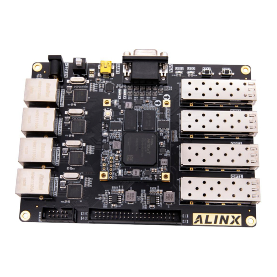
Part 1: FPGA Development Board Introduction..........6 Part 2: AC7100B core board..........错误!未定义书签。 Part 2.1: AC7100B Core Board Introduction...错误!未定义书签。 Part 2.2: FPGA Chip............错误!未定义书签。 Part 2.3: Active Differential Crystal......错误!未定义书签。...
  • Page 4 ARTIX-7 FPGA Development Board AX7101 User Manual www.alinx.com 4 / 51...
  • Page 5 In the design of carrier Board, we have extended 4 fiber interfaces and 4 Gigabit Ethernet interfaces. It meets user's requirements for high-speed data transmission and exchange. It is a "Versatile" and “Professional” ARTIX-7 FPGA development platform. It provides the applications for multi-channel video transmission, multi-channel networks, fiber-optic communication, and data processing.
  • Page 6: Part 1: Fpga Development Board Introduction

    /s(800M*32bit); The two DDR3 capacities are up to 8Gbit, which meets the need for high buffers during data processing. The selected FPGA is the XC7A100T chip of XILINX's ARTIX-7 series, in BGA 484 package. The communication frequency between the XC7A100T and DDR3 reaches 400Mhz and the data rate is 800Mhz, which fully meets the needs of high-speed multi-channel data processing.
  • Page 7 ARTIX-7 FPGA Development Board AX7101 User Manual Figure 1-1-1: The Schematic Diagram of the AX7101 Through this diagram, you can see the interfaces and functions that the AX7101 FPGA Development Board contains:  Artix-7 FPGA core board The core board consists of XC7A100T + 8Gb DDR3 + 128Mb QSPI FLASH.
  • Page 8 ARTIX-7 FPGA Development Board AX7101 User Manual  4-channel high-speed SFP Interface The four high-speed transceivers of the GTP transceiver of ARTIX-7 FPGA are connected to the transmission and reception of four optical modules to realize four high-speed optical fiber communication interfaces.
  • Page 9: Part 2: Ac7100B Core Board

    Part 2.1: AC7100B Core Board Introduction AC7100B (core board model, the same below) FPGA core board, it is based on XILINX's ARTIX-7 series 100T XC7A100T-2FGG484I. It is a high-performance core board with high speed, high bandwidth and high capacity. It is suitable for high-speed data communication, video image processing, high-speed data acquisition, etc.
  • Page 10 ARTIX-7 FPGA Development Board AX7101 User Manual Figure 2-1-1: AC7100B Core Board (Front View) Figure 2-1-2: AC7100B Core Board (Rear View) www.alinx.com 10 / 51...
  • Page 11: Part 2.2: Fpga Chip

    Part 2.2: FPGA Chip As mentioned above, the FPGA model we use is XC7A100T-2FGG484I, which belongs to Xilinx's Artix-7 series. The speed grade is 2, and the temperature grade is industry grade. This model is a FGG484 package with 484 pins. Xilinx ARTIX-7 FPGA chip naming rules as below...
  • Page 12: Part 2.3: Active Differential Crystal

    FPGA internal GTP transceiver, connected to 1.0V; VMGTAVTT is the termination voltage of the GTP transceiver, connected to 1.2V. The Artix-7 FPGA system requires that the power-up sequence be powered by VCCINT, then VCCBRAM, then VCCAUX, and finally VCCO. If VCCINT and VCCBRAM have the same voltage, they can be powered up at the same time.
  • Page 13 ARTIX-7 FPGA Development Board AX7101 User Manual BANK34 global clock pin MRCC (R4 and T4) of the FPGA. This 200Mhz differential clock can be used to drive the user logic in the FPGA. Users can configure the PLLs and DCMs inside the FPGA to generate clocks of different frequencies.
  • Page 14 ARTIX-7 FPGA Development Board AX7101 User Manual output is connected to the GTP BANK216 clock pins MGTREFCLK0P (F6) and MGTREFCLK0N (E6) of the FPGA. Figure 2-3-3: 125Mhz Active Differential Crystal Schematic Figure 2-3-4: 125Mhz Active Differential Crystal on the Core Board...
  • Page 15: Part 2.4: Ddr3 Dram

    ARTIX-7 FPGA Development Board AX7101 User Manual Part 2.4: DDR3 DRAM The FPGA core board AC7100B is equipped with two Micron 4Gbit (512MB) DDR3 chips, model MT41J256M16HA-125 (compatible with MT41K256M16HA-125). The DDR3 SDRAM has a maximum operating speed of 800MHz (data rate 1600Mbps). The DDR3 memory system is directly connected to the memory interface of the BANK 34 and BANK35 of the FPGA.
  • Page 16 ARTIX-7 FPGA Development Board AX7101 User Manual Figure 2-4-2: The DDR3 on the Core Board DDR3 DRAM pin assignment: Net Name FPGA PIN Name FPGA P/N DDR3_DQS0_P IO_L3P_T0_DQS_AD5P_35 DDR3_DQS0_N IO_L3N_T0_DQS_AD5N_35 DDR3_DQS1_P IO_L9P_T1_DQS_AD7P_35 DDR3_DQS1_N IO_L9N_T1_DQS_AD7N_35 DDR3_DQS2_P IO_L15P_T2_DQS_35 DDR3_DQS2_N IO_L15N_T2_DQS_35 DDR3_DQS3_P IO_L21P_T3_DQS_35...
  • Page 17: Part 2.5: Qspi Flash

    ARTIX-7 FPGA Development Board AX7101 User Manual DDR3_DQ [4] IO_L2N_T0_AD12N_35 DDR3_DQ [5] IO_L5N_T0_AD13N_35 DDR3_DQ [6] IO_L1P_T0_AD4P_35 DDR3_DQ [7] IO_L4P_T0_35 DDR3_DQ [8] IO_L11P_T1_SRCC_35 DDR3_DQ [9] IO_L11N_T1_SRCC_35 DDR3_DQ [10] IO_L8P_T1_AD14P_35 DDR3_DQ [11] IO_L10N_T1_AD15N_35 DDR3_DQ [12] IO_L7N_T1_AD6N_35 DDR3_DQ [13] IO_L10P_T1_AD15P_35 DDR3_DQ [14] IO_L7P_T1_AD6P_35...
  • Page 18 ARTIX-7 FPGA Development Board AX7101 User Manual the FPGA chip. The clock pin is connected to CCLK0 of BANK0, and other data and chip select signals are connected to D00~D03 and FCS pins of BANK14 respectively. Figure 2-5-1 shows the hardware connection of QSPI Flash.
  • Page 19: Part 2.6: Led Light On Core Board

    ARTIX-7 FPGA Development Board AX7101 User Manual Part 2.6: LED Light on Core Board There are 3 red LED lights on the AC7100B FPGA core board, one of which is the power indicator light (PWR), one is the configuration LED light (DONE), and one is the user LED light.
  • Page 20: Part 2.8: Jtag Interface

    ARTIX-7 FPGA Development Board AX7101 User Manual the reset key connection is shown in Figure 2-7-1: Figure 2-7-1: Reset key Schematic Figure 2-7-2: Reset key on the Core Board Reset key pin assignment Signal Name ZYNQ Pin Name ZYNQ Pin Number...
  • Page 21: Part 2.9: Power Interface On The Core Board

    ARTIX-7 FPGA Development Board AX7101 User Manual The JTAG interface J1 on AC7100B FPGA core board uses a 6-pin 2.54mm pitch single-row test hole. If you need to use the JTAG connection to debug on the core board, you need to solder a 6-pin single-row pin header.
  • Page 22 ARTIX-7 FPGA Development Board AX7101 User Manual Figure 2-9-2:J3 interface on the Core Board Part 2.10: Board to Board Connectors pin assignment The core board has a total of four high-speed board to board connectors. The core board uses four 80-pin inter-board connectors to connect to the carrier board.
  • Page 23 ARTIX-7 FPGA Development Board AX7101 User Manual Pin Assignment of Board to Board Connectors CON1 CON1 Signal Name FPGA Pin Voltage CON1 Signal Name FPGA Pin Voltage Level Level PIN1 VCCIN PIN2 VCCIN PIN3 VCCIN PIN4 VCCIN PIN5 VCCIN PIN6...
  • Page 24 ARTIX-7 FPGA Development Board AX7101 User Manual PIN59 Ground PIN60 Ground PIN61 B16_L1_N 3.3V PIN62 PIN63 B16_L1_P 3.3V PIN64 PIN65 B16_L4_N 3.3V PIN66 PIN67 B16_L4_P 3.3V PIN68 PIN69 Ground PIN70 Ground PIN71 B16_L6_N 3.3V PIN72 Board to Board Connectors CON2 The 80-pin female connection header CON2 is used to extend the normal IO of the BANK13 and BANK14 of the FPGA.
  • Page 25 ARTIX-7 FPGA Development Board AX7101 User Manual PIN33 B13_L9_P AA10 3.3V PIN34 B13_IO0 3.3V PIN35 B13_L8_N AB10 3.3V PIN36 B14_L7_N 3.3V PIN37 B13_L8_P 3.3V PIN38 B14_L7_P 3.3V PIN39 Ground PIN40 Ground PIN41 B14_L11_N 3.3V PIN42 B14_L4_P 3.3V PIN43 B14_L11_P 3.3V...
  • Page 26 ARTIX-7 FPGA Development Board AX7101 User Manual a suitable LDO. Pin Assignment of Board to Board Connectors CON3 CON1 Signal Name FPGA CON1 Signal Name FPGA Pin Voltage Voltage Level Level PIN1 B15_IO0 3.3V PIN2 B15_IO25 3.3V PIN3 B16_IO0 3.3V...
  • Page 27 ARTIX-7 FPGA Development Board AX7101 User Manual PIN57 B15_L21_N 3.3V PIN58 B15_L10_N 3.3V PIN59 Ground PIN60 Ground PIN61 B15_L23_P 3.3V PIN62 B15_L18_P 3.3V PIN63 B15_L23_N 3.3V PIN64 B15_L18_N 3.3V PIN65 B15_L22_P 3.3V PIN66 B15_L17_N 3.3V PIN67 B15_L22_N 3.3V PIN68 B15_L17_P 3.3V...
  • Page 28 ARTIX-7 FPGA Development Board AX7101 User Manual PIN15 Ground PIN16 Ground PIN17 MGT_TX3_P Differential PIN18 MGT_RX2_P Differential PIN19 MGT_TX3_N Differential PIN20 MGT_RX2_N Differential PIN21 Ground PIN22 Ground PIN23 MGT_RX3_P Differential PIN24 MGT_TX0_P Differential PIN25 MGT_RX3_N Differential PIN26 MGT_TX0_N Differential PIN27...
  • Page 29: Part 2.11: Power Supply

    ARTIX-7 FPGA Development Board AX7101 User Manual PIN79 PIN80 Part 2.11: Power Supply The AC7100B FPGA core board is powered by DC5V via carrier board, and it is powered by the J3 interface when it is used alone. Please be careful not to supply power to J3 interface and the carrier board at the same time to avoid damage.
  • Page 30 MGTVCCAUX(+1.8V) GTP Transceiver Bank216 of FPGA Because the power supply of Artix-7 FPGA has the power-on sequence requirement, in the circuit design, we have designed according to the power requirements of the chip, and the power-on is 1.0V->1.8V->(1.5 V, 3.3V, VCCIO) and 1.0V->...
  • Page 31: Part 2.12: Structure Diagram

    ARTIX-7 FPGA Development Board AX7101 User Manual Part 2.12: Structure Diagram Figure 2-12-1: AC7100B FPGA Core board (Top view) Figure 2-12-2: AC7100B FPGA Core board (Bottom view) www.alinx.com 31 / 51...
  • Page 32: Part 3: Carrier Board

    ARTIX-7 FPGA Development Board AX7101 User Manual Part 3: Carrier Board Part 3.1: Carrier Board Introduction Through the previous function introduction, you can understand the function of the carrier board part  4-channel 10/100M/1000M Ethernet RJ-45 interface  4-channel SFP interface ...
  • Page 33: Part 3.2: Gigabit Ethernet Interface

    ARTIX-7 FPGA Development Board AX7101 User Manual Part 3.2: Gigabit Ethernet Interface The AX7101 FPGA carrier board provides users with 4-channel Gigabit network communication service through the Realtek RTL8211EG Ethernet PHY chip. The RTL8211EG chip supports 10/100/1000 Mbps network transmission rate and communicates with the FPGA through the GMII interface.
  • Page 34 ARTIX-7 FPGA Development Board AX7101 User Manual sampled on the rising edge of the clock. Figure 3-2-1: Gigabit Ethernet Interface Schematic Figure 3-3-2: Gigabit Ethernet interface on the Carrier Board www.alinx.com 34 / 51...
  • Page 35 ARTIX-7 FPGA Development Board AX7101 User Manual The 1 channel Gigabit Ethernet pin assignments are as follows: Signal Name FPGA Pin Description E1_GTXC Ethernet GMII transmit clock E1_TXD0 Ethernet Transmit Data bit0 E1_TXD1 Ethernet Transmit Data bit1 E1_TXD2 Ethernet Transmit Data bit2...
  • Page 36 ARTIX-7 FPGA Development Board AX7101 User Manual The 2 channel Gigabit Ethernet pin assignments are as follows: Signal Name FPGA Pin Description E2_GTXC Ethernet GMII transmit clock E2_TXD0 Ethernet Transmit Data bit0 E2_TXD1 Ethernet Transmit Data bit1 E2_TXD2 Ethernet Transmit Data bit2...
  • Page 37 ARTIX-7 FPGA Development Board AX7101 User Manual The 3 channel Gigabit Ethernet pin assignments are as follows: Signal Name FPGA Pin Description E3_GTXC AA21 Ethernet GMII transmit clock E3_TXD0 Ethernet Transmit Data bit0 E3_TXD1 Ethernet Transmit Data bit1 E3_TXD2 Ethernet Transmit Data bit2...
  • Page 38 ARTIX-7 FPGA Development Board AX7101 User Manual The 4 channel Gigabit Ethernet pin assignments are as follows: Signal Name FPGA Pin Description E4_GTXC Ethernet GMII transmit clock E4_TXD0 Ethernet Transmit Data bit0 E4_TXD1 Ethernet Transmit Data bit1 E4_TXD2 Ethernet Transmit Data bit2...
  • Page 39: Part 3.3: Sfp Interface

    ARTIX-7 FPGA Development Board AX7101 User Manual Part 3.3: SFP Interface The AX7101 FPGA carrier board has four optical interfaces. Users can purchase SFP optical modules (1.25G, 2.5G optical modules on the market) and insert them into these four optical interfaces for optical data communication.
  • Page 40 ARTIX-7 FPGA Development Board AX7101 User Manual Figure 3-3-2: SFP interfaces on the Carrier Board The 1 fiber interface FPGA pin assignment is as follows: Signal Name FPGA PIN Description SFP1_TX_P SFP1 Data Transfer (Positive) SFP1_TX_N SFP1 Data Transfer (Negative)
  • Page 41: Part 3.4: Vga Display Interface

    ARTIX-7 FPGA Development Board AX7101 User Manual The 2 fiber interface FPGA pin assignment is as follows: Signal Name FPGA PIN Description SFP2_TX_P SFP2 Data Transfer (Positive) SFP2_TX_N SFP2 Data Transfer (Negative) SFP2_RX_P SFP2 Data Receiver (Positive) SFP2_RX_P SFP2 Data Receiver (Negative)
  • Page 42 ARTIX-7 FPGA Development Board AX7101 User Manual VSYNC pins. Pins 1, 2, and 3 are red, green, and blue primary color analog voltages, which are 0 to 0.714V peak-peak, 0V is colorless, and 0.714V is full color. Some non-standard displays use a full color level of 1Vpp. The three primary color source terminals and terminal matching resistors are both 75 ohms.
  • Page 43 ARTIX-7 FPGA Development Board AX7101 User Manual Figure 3-4-2: VGA Display Interface Schematic Figure 3-4-3: VGA Display Interface on the Carrier Board VGA Pin Assignment: Signal Name FPGA Pin Description VGA_B[0] BLUE[0] VGA_B[1] BLUE[1] VGA_B[2] BLUE[2] VGA_B[3] BLUE[3] www.alinx.com 43 / 51...
  • Page 44: Part 3.5: Usb To Serial Port

    ARTIX-7 FPGA Development Board AX7101 User Manual VGA_B[4] BLUE[4] VGA_G[0] GREEN[0] VGA_G[1] AB13 GREEN[1] VGA_G[2] GREEN[2] VGA_G[3] AA14 GREEN[3] VGA_G[4] AA13 GREEN[4] VGA_G[5] AB12 GREEN[5] VGA_R[0] AB16 RED[0] VGA_R[1] RED[1] VGA_R[2] AA16 RED[2] VGA_R[3] RED[3] VGA_R[4] AB17 RED[4] VGA_HS Horizontal sync signal...
  • Page 45 ARTIX-7 FPGA Development Board AX7101 User Manual Figure 3-5-2: USB to serial port on the Carrier Board Two LED indicators (LED4 and LED3) are set for the serial port signal, and the silkscreen on the PCB is TX and RX, indicating that the serial port has data...
  • Page 46: Part 3.6: Expansion Header

    Part 3.6: Expansion Header The AX7101 FPGA carrier board is reserved with one 0.1inch spacing standard 40-pin expansion header J11 which is used to connect the ALINX modules or the external circuit designed by the user. The expansion port has 40 signals, of which 1-channel 5V power supply, 2-channel 3.3 V power supply,...
  • Page 47: Part 3.7: Jtag Interface

    ARTIX-7 FPGA Development Board AX7101 User Manual J11 Expansion Header Pin Assignment J11 Pin Number FPGA Pin J11 Pin Number FPGA Pin +3.3V +3.3V Part 3.7: JTAG Interface A JTAG interface is reserved on the AX7101 FPGA carrier board for downloading FPGA programs or firmware to FLASH.
  • Page 48: Part 3.8: Keys

    ARTIX-7 FPGA Development Board AX7101 User Manual Figure 3-7-1: JTAG Interface Schematic Figure 3-7-2: JTAG Interface on the Carrier Board Be careful not to hot swap when JTAG cable is plugged and unplugged. Part 3.8: Keys The AX7101 FPGA carrier board contains two user Keys KEY1~KEY2. All Keys are connected to the normal IO of the FPGA.
  • Page 49: Part 3.9: Led Light

    ARTIX-7 FPGA Development Board AX7101 User Manual Figure 3-8-1: Key Schematic Figure 3-8-2: Four Keys on the carrier board Keys Pin Assignment Net Name FPGA PIN KEY1 KEY2 Part 3.9: LED Light There are three red LEDs on the AX7101 FPGA Carrier Board, one of which is the power indicator (PWR), two are users LED lights (LED1~LED2).
  • Page 50: Part 3.10: Power Supply

    ARTIX-7 FPGA Development Board AX7101 User Manual Figure 3-9-1: The User LEDs Schematic Figure 3-9-2: The User LEDs on the Carrier Board Pin assignment of user LED lights Signal Name FPGA PIN KEY1 KEY2 Part 3.10: Power Supply The power input voltage of the The AX7101 FPGA carrier board is DC12V.
  • Page 51 ARTIX-7 FPGA Development Board AX7101 User Manual Figure 3-10-1 Power Design Schematic on the Carrier Board Figure 3-10-2: Power circuit on the Carrier Board www.alinx.com 51 / 51...

This manual is also suitable for:

Ax7101

Table of Contents