Table of Contents
Advertisement
Quick Links
Advertisement
Table of Contents

Related Manuals for Alinx AX7021


Summary of Contents for Alinx AX7021
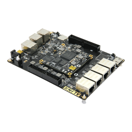
- Page 1 ZYNQ7000 FPGA Development Board AX7021 User Manual...
-
Page 2: Version Record
ZYNQ FPGA Development Board AX7021 User Manual Version Record Version Date Release By Description Rev 1.0 2019-03-27 Rachel Zhou First Release Rev 1.1 2020-09-21 Rachel Zhou Correct the corresponding pins of B34_L15_N/P. Amazon Store: https://www.amazon.com/alinx 2 / 57... -
Page 3: Table Of Contents
ZYNQ FPGA Development Board AX7021 User Manual Table of Contents Version Record....................... 2 Part 1: FPGA Development Board Introduction............. 6 Part 2: AC7021 Core Board..................8 2.1 Introduction......................8 2.2 ZYQN Chip...................... 10 2.3 DDR3 DRAM....................13 2.4 QSPI Flash...................... 16 2.5 eMMC Flash.................... - Page 4 ZYNQ FPGA Development Board AX7021 User Manual 3.11 Power Supply....................52 3.12 Carrier Board Structure diagram............... 54 Amazon Store: https://www.amazon.com/alinx 4 / 57...
- Page 5 ZYNQ FPGA Development Board AX7021 User Manual This ZYNQ7000 FPGA development platform adopts the core board + carrier board mode, which is convenient for users to use the core board for secondary development. The core board uses XILINX's Zynq7000 SOC chip solution, which combines dual-core ARM Cortex-A9 and FPGA programmable logic on a single chip using ARM+FPGA SOC technology.
-
Page 6: Part 1: Fpga Development Board Introduction
HDMI output interface, 1-port SD Card interface, 1-port UART USB serial port interface, 1-port SD Card interface, 2-port 40-pin carrier headers and some button LEDs. Figure 1-1-1 is the block diagram of the FPGA development board AX7021: Amazon Store: https://www.amazon.com/alinx 6 / 54... - Page 7 ZYNQ FPGA Development Board AX7021 User Manual Figure 1-1-1: The block diagram of AX7021 The interfaces and features included in the development board. ZYNQ7000 Core Board It consists of XC7Z020+1GB DDR3+32GB eMMC FLASH + 256Mb QSPI FLASH. In addition, two crystal oscillators provide clocks, one is 33.3333MHz for PS system and the other is 50MHz for PL logic.
-
Page 8: Part 2: Ac7021 Core Board
ZYNQ FPGA Development Board AX7021 User Manual USB Interface 1 JTAG debug interface, using MINI USB interface, users can debug and download ZYNQ system through USB cable and onboard JTAG circuit. LED Light 9 LEDs, include 6 on the core board and 3 on the extension board. There are 1 power indicator, 1 DONE configuration indicator, 2 user indicators and 2 serial port transceiver indicators on the core board. - Page 9 ZYNQ FPGA Development Board AX7021 User Manual LDO chip on the core board to meet the requirements of users with different level interfaces. For users who need a lot of IOs, this core board will be a good choice. Moreover, the IOs connection part, the routing between the ZYNQ FPGA chip and the interface is equal length and differential processing.
-
Page 10: Zyqn Chip
ZYNQ FPGA Development Board AX7021 User Manual Figure 2-2-2:AC7021 core board rear view 2.2 ZYQN Chip The development board uses Xilinx's Zynq7000 series chip, model XC7Z020-2CLG484I. The chip's PS system integrates two ARM CortexTM-A9 processors, AMBA® interconnects, internal memory, external memory interfaces and peripherals. - Page 11 ZYNQ FPGA Development Board AX7021 User Manual Figure 2-2-3: Overall Block Diagram of the ZYNQ7000 Chip The main parameters of the PS system part are as follows: ARM dual-core CortexA9-based application processor, ARM-v7 architecture, up to 1GHz 32KB level 1 instruction and data cache per CPU, 512KB level 2 cache 2...
- Page 12 ZYNQ FPGA Development Board AX7021 User Manual The main parameters of the PL logic part are as follows: LogicCells: 85K Look-up-tables (LUTs):53,200 Flip-flops:106,400 18x25MACCs:220; BlockRAM:4.9Mb Two AD converters for on-chip voltage, temperature sensing and up...
-
Page 13: Ddr3 Dram
ZYNQ FPGA Development Board AX7021 User Manual Figure 2-2-5: TheXC7Z020 chip used on the Core Board 2.3 DDR3 DRAM The AC7021 core board is equipped with two SK Hynix DDR3 SDRAM chips (1GB total), model H5TQ4G63AFR-PBI. The bus width of DDR3 SDRAM is 32 bits in total. - Page 14 ZYNQ FPGA Development Board AX7021 User Manual The hardware connection of DDR3 DRAM is shown in Figure 2-3-1: Figure 2-3-1: The Schematic part of DDR3 DRAM Figure 2-3-2: DDR3 DRAM on the Core Board Amazon Store: https://www.amazon.com/alinx 14 / 54...
- Page 15 ZYNQ FPGA Development Board AX7021 User Manual DDR3 DRAM Pin Assignment Signal Name ZYNQ Pin Name Pin Number DDR3_DQS0_P PS_DDR_DQS_P0_502 DDR3_DQS0_N PS_DDR_DQS_N0_502 DDR3_DQS1_P PS_DDR_DQS_P1_502 DDR3_DQS1_N PS_DDR_DQS_N1_502 DDR3_DQS2_P PS_DDR_DQS_P2_502 DDR3_DQS2_N PS_DDR_DQS_N2_502 DDR3_DQS3_P PS_DDR_DQS_P3_502 DDR3_DQS4_N PS_DDR_DQS_N3_502 DDR3_D0 PS_DDR_DQ0_502 DDR3_D1 PS_DDR_DQ1_502 DDR3_D2 PS_DDR_DQ2_502...
-
Page 16: Qspi Flash
ZYNQ FPGA Development Board AX7021 User Manual DDR3_A9 PS_DDR_A9_502 DDR3_A10 PS_DDR_A10_502 DDR3_A11 PS_DDR_A11_502 DDR3_A12 PS_DDR_A12_502 DDR3_A13 PS_DDR_A13_502 DDR3_A14 PS_DDR_A14_502 DDR3_BA0 PS_DDR_BA0_502 DDR3_BA1 PS_DDR_BA1_502 DDR3_BA2 PS_DDR_BA2_502 DDR3_S0 PS_DDR_CS_B_502 DDR3_RAS PS_DDR_RAS_B_502 DDR3_CAS PS_DDR_CAS_B_502 DDR3_WE PS_DDR_WE_B_502 DDR3_ODT PS_DDR_ODT_502 DDR3_RESET PS_DDR_DRST_B_502 DDR3_CLK0_P PS_DDR_CKP_502 DDR3_CLK0_N... -
Page 17: Emmc Flash
ZYNQ FPGA Development Board AX7021 User Manual Figure 2-4-1: QSPI Flash in the schematic Figure 2-4-2: QSPI Flash on the Core Board Pin Assignment of QSPI Flash Signal Name ZYNQ Pin Name Pin Number QSPI_SCK PS_MIO6_500 QSPI_CS PS_MIO1_500 QSPI_D0 PS_MIO2_500... - Page 18 ZYNQ FPGA Development Board AX7021 User Manual non-volatile nature of eMMC FLASH, it can be used as a large-capacity storage device for the ZYNQ system, such as ARM-based applications, system files, and other user data files. The specific models and related parameters of eMMC FLASH are shown in Table 2-5-1:...
-
Page 19: Clock Configuration
ZYNQ FPGA Development Board AX7021 User Manual Pin Assignment of eMMC Flash Signal Name ZYNQ Pin Name Pin Number MMC_CCLK PS_MIO48_501 MMC_CMD PS_MIO47_501 MMC_D0 PS_MIO46_501 MMC_D1 PS_MIO49_501 MMC_D2 PS_MIO50_501 MMC_D3 PS_MIO51_501 Table 2-5-2: Pin Assignment of eMMC FLASH 2.6 Clock configuration... -
Page 20: Usb To Serial Port
ZYNQ FPGA Development Board AX7021 User Manual PS Clock pin assignment: Signal Name PS_CLK_500 Table 2-6-1: PS Clock pin assignment PL system clock source The AC7021 core board provides a single-ended 50MHz PL system clock source with 3.3V power supply. The crystal output is connected to the global clock (MRCC) of the FPGA BANK13, which can be used to drive user logic within the FPGA. - Page 21 ZYNQ FPGA Development Board AX7021 User Manual can be connected to the USB port of the upper PC with a USB cable for separate power supply and serial data communication of the core board. Figure 2-7-1: USB to Serial Port...
-
Page 22: Led
ZYNQ FPGA Development Board AX7021 User Manual Uart Pin Assignment: Signal Name Pin Name Pin Number Explain UART_RXD PS_MIO14_500 Uart data output UART_TXD PS_MIO15_500 Uart data input Table 2-7-1: Uart Pin Assignment 2.8 LED There are 6 red LED lights on the AC7021 core board, one of which is the... -
Page 23: Reset Button
ZYNQ FPGA Development Board AX7021 User Manual Figure 2-8-2: The LEDs on the Core Board LED Pin Assignment: Signal Name Pin Name Pin Number Explain MIO0_LED PS_MIO0_500 User LED1 PL_LED IO_0_13 User LED2 Table 2-8-1: LED Pin Assignment 2.9 Reset button The AC7021 has a reset button RESET and circuitry on the core board. -
Page 24: Jtage Interface
ZYNQ FPGA Development Board AX7021 User Manual Figure 2-9-1: Reset button connection diagram Figure 2-9-2: Reset Button on the Core Board Reset Pin Assignment: Signal Name Pin Name Pin Number Explain PS_POR_B PS_POR_B_500 Reset Key Table 2-9-1: Reset Pin Assignment 2.10 JTAGE Interface... -
Page 25: Dip Switch Configuration
ZYNQ FPGA Development Board AX7021 User Manual The JTAG interface J1 on the core board uses a 6-pin 2.54mm pitch single-row test hole. If you need to use the JTAG connection to debug on the core board, you need to solder a 6-pin single-row pin header. Figure 2-10-2 shows the physical map of the JTAG interface on the development board. - Page 26 ZYNQ FPGA Development Board AX7021 User Manual USB and the extension board at the same time to avoid damage. The power supply design on the core board is shown in Figure 2-12-1. Figure 2-12-1: The Power Supply Design on the Core Board The development board is powered by +5V, and is converted into +1.0V,...
- Page 27 ZYNQ FPGA Development Board AX7021 User Manual Power Function +1.0V ZYNQ PS and PL section core voltage +1.8V ZYNQ PS and PL partial auxiliary voltage, BANK501 IO voltage, eMMC +3.3V ZCNQ Bank0, Bank500, Bank13, Bank35, VCCIO,QSIP FLASH, Clock Crystal +1.5V...
-
Page 28: Structure Diagram
ZYNQ FPGA Development Board AX7021 User Manual 2.13 Structure diagram Figure 2-13-1: The Structure diagram (Top View) 2.14 Connector pin definition The core board expands four high-speed carrier ports, and uses four 80Pin inter-board connectors (CON1~CON4) to connect with the backplane. The PIN pitch of the connector is 0.5mm. - Page 29 ZYNQ FPGA Development Board AX7021 User Manual CON1 Pin Signal Name CON1 Pin Signal Name ZYNQ Pin ZYNQ Pin PS_MIO13 ETH_TXD0 PS_MIO12 ETH_TXD1 ETH_TXD2 ETH_TXD3 ETH_TXCK ETH_TXCTL ETH_RXD3 ETH_RXD2 PS_MIO7 ETH_RXD1 PS_MIO8 ETH_RXD0 PS_MIO9 ETH_RXCTL PS_MIO11 ETH_RXCK ETH_MDC ETH_MDIO OTG_STP...
- Page 30 ZYNQ FPGA Development Board AX7021 User Manual SD_D1 OTG_DATA3 SD_D0 OTG_DATA4 SD_CMD OTG_DATA5 SD_D3 OTG_DATA6 SD_D2 OTG_DATA7 FPGA_TMS FPGA_TCK FPGA_TDO FPGA_TDI Table 2-14-1: Pin Assignment of CON1 ZYNQ Pin ZYNQ Pin CON2 Pin Singal Name CON2 Pin Singal Name B13_L1_N...
- Page 31 ZYNQ FPGA Development Board AX7021 User Manual B33_L11_P B13_L20_P B33_L11_N AA19 B13_L20_N B33_L5_P B13_L3_P B33_L5_N B13_L3_N B33_L1_P B13_L10_P B33_L1_N B13_L10_N B13_L7_P AA12 B13_L2_P B13_L7_N AB12 B13_L2_N B13_L8_N AB11 B13_L14_P B13_L8_P AA11 B13_L14_N B13_L9_N B13_L16_P B13_L9_P AB10 B13_L16_N B13_L11_N B13_L18_N B13_L11_P...
- Page 32 ZYNQ FPGA Development Board AX7021 User Manual B34_L1_P B34_L15_N B34_L1_N B34_L15_P B34_L17_P B34_L16_P B34_L17_N B34_L16_N B34_L14_N B34_L20_N B34_L14_P B34_L20_P B34_L5_N B34_L13_P B34_L5_P B34_L13_N B33_L9_P B34_L21_N B33_L9_N B34_L21_P B33_L8_P AA21 B33_L6_N B33_L8_N AB21 B33_L6_P B33_L12_N AA18 B33_L16_P B33_L12_P B33_L16_N B33_L13_P B33_L17_N...
- Page 33 ZYNQ FPGA Development Board AX7021 User Manual B34_IO0 B33_IO0 Table 2-14-3: Pin Assignment of CON3 ZYNQ Pin ZYNQ Pin CON4 Pin Signal Name CON4 Pin Signal Name B35_L7_N B35_L9_P B35_L7_P B35_L9_N B35_L8_P B35_L10_P B35_L8_N B35_L10_N B35_L11_N B35_L15_P B35_L11_P B35_L15_N B35_L13_N...
- Page 34 ZYNQ FPGA Development Board AX7021 User Manual B35_L4_N B34_L9_N B35_L3_N B35_IO25 B35_L3_P B35_IO0 B34_L24_N B34_L4_P B34_L24_P B34_L4_N B34_L23_P B34_L18_N B34_L23_N B34_L18_P B35_L5_P B34_L22_P B35_L5_N B34_L22_N B34_L19_P B34_L19_N Table 2-14-4: Pin Assignment of CON4 Amazon Store: https://www.amazon.com/alinx 34 / 54...
-
Page 35: Part 3: Carrier Board
ZYNQ FPGA Development Board AX7021 User Manual Part 3: Carrier Board 3.1 Carrier Board Introduction Through the previous function introduction, we can understand the function of the carrier board. 5 ports 10/100M/1000M Ethernet RJ-45 interface 1 port HDMI output display interface ... -
Page 36: Gigabit Ethernet Interface
ZYNQ FPGA Development Board AX7021 User Manual 3.2 Gigabit Ethernet interface The AX7021 has five Gigabit Ethernet interfaces on the carrier board, one of which is the connected PS system side. The Ethernet interface is connected to the logical IO port of the PL. The 4-port Gigabit Ethernet interface connected to the PL side needs to be mounted to ZYNQ's AXI bus system by call IP program. - Page 37 ZYNQ FPGA Development Board AX7021 User Manual ZYNQ and PHY chip KSZ9031RNX is communicated through the RMII bus, and the transmission clock is 25Mhz. Data is sampled on the rising edge and falling samples of the clock. Figure 3-2-1 and Figure 3-2-2 detailed the...
- Page 38 ZYNQ FPGA Development Board AX7021 User Manual Figure 3-2-3: PS side Ethernet GPHY port on Carrier board Figure 2-3-4: 4 PS side Ethernet GPHY port on the carrier port ETH0(PS) Pin Assignment: Signal Name Pin Name Pin Number Explain PHY1_TXCK...
- Page 39 ZYNQ FPGA Development Board AX7021 User Manual ETH1(PL) Pin Assignment: Signal Name Pin Name Pin Number Explain PHY2_TXCK B34_L17_N RGMII Send clock PHY2_TXD0 B34_L5_P Send data bit0 PHY2_TXD1 B34_L5_N Send data bit1 PHY2_TXD2 B34_L14_P Send data bit2 PHY2_TXD3 B34_L14_N Send data bit3...
-
Page 40: Usb2.0 Host Interface
MDIO Management data 3.3 USB2.0 Host interface There are 4 USB2.0 HOST interfaces on the AX7021 carrier board. The USB2.0 transceiver uses a 1.8V, high-speed USB3320C-EZK chip that supports the ULPI standard interface, and then expands the 4-port USB HOST interface through a USB HUB chip USB2514. - Page 41 ZYNQ FPGA Development Board AX7021 User Manual Figure 3-3-1: The connection between Zynq7000 and USB chip Figure 3-3-2 shows the physical picture of the USB2.0 chip and interface, where the USB interface uses a dual USB interface. Figure 3-3-2: The USB2.0 on the Carrier Board USB2.0 Pin Assignment:...
-
Page 42: Hdmi Output Interface
ZYNQ FPGA Development Board AX7021 User Manual OTG_DATA0 PS_MIO32_501 USB data bit0 OTG_DATA1 PS_MIO33_501 USB data bit1 OTG_DATA2 PS_MIO34_501 USB data bit2 OTG_DATA3 PS_MIO35_501 USB data bit3 OTG_CLK PS_MIO36_501 USB clock signal OTG_DATA5 PS_MIO37_501 USB data bit5 OTG_DATA6 PS_MIO38_501 USB data bit6... - Page 43 ZYNQ FPGA Development Board AX7021 User Manual Figure3-4-2: The HDMI Interface on the Carrier Board HDMI out Pin Assignment: Signal Name Pin Name Pin Number Explain 9134_CLK B35_L4_N clock 9134_HS B35_L21_P line synchronization 9134_VS B35_L1_P column synchronization 9134_DE B35_L21_N Signal valid...
-
Page 44: Usb To Serial Port
IIC Control data 3.5 USB to serial port The AX7021 carrier board is also equipped with a serial port interface for overall debugging of the ZYNQ7000 system. The conversion chip uses the USB-UAR chip of Silicon Labs CP2102GM. The USB interface uses the MINI USB interface. -
Page 45: Sd Card Slot
Uart data output 3.6 SD card slot The AX7021 carrier board contains a Micro SD card interface to provide user access to the SD card memory, the BOOT program for the ZYNQ chip, the Linux operating system kernel, the file system and other user data files. -
Page 46: Jtag Interface
USB of PC and ZYNQ JTAG debug signals TCK, TDO, TMS, TDI are used for data communication via the FTDI USB bridge chip FT232HL on the development board. On the AX7021 development board, the JTAG interface is in the USB interface mode. Users can connect the PC and JTAG interface to the ZYNQ system debugging through the USB cable provided by us. -
Page 47: Led
Figure 3-7-2: JTAG Interface on the Carrier Board 3.8 LED The AX7021 has three red LEDs on the carrier board, one of which is the power indicator (PWR) and two of which are user LEDs (LED1~LED2). When the carrier board is powered, the power indicator will light up; two user LEDs are connected to the MIO of the PS, and one is connected to the IO of the PL. -
Page 48: User Button
PL LED 3.9 User Button The AX7021 has two user buttons KEY1 and KEY2 on the carrier board. KEY1 is connected to the MIO pin of the ZYNQ chip PS, and KEY2 is connected to the IO pin of the ZYNQ chip PL. When the button is pressed, the signal is low, and the ZYNQ chip detects a low level to determine whether the button is pressed. -
Page 49: Extension Port
PL User Key 3.10 Extension Port The AX7021 carrier board is reserved with two 2.54-mm standard 40-pin expansion ports J15 and J16 for connecting various modules of ALINX or external circuits designed by the user. The expansion port has 40 signals, of which 1 channel is 5V power supply. - Page 50 ZYNQ FPGA Development Board AX7021 User Manual Figure 3-10-1: The Expansion Port J15 Schematic Figure 3-10-2 shows the physical map of the J15 expansion port. Pin39 and Pin40 of the expansion port are indicated on the board. Figure 3-10-2: The J15 Expansion Port on the Carrier Board...
- Page 51 ZYNQ FPGA Development Board AX7021 User Manual AB19 AB20 AA21 AB21 +3.3V +3.3V(Output) Figure 3-10-3: The Expansion Port J16 Schematic Figure 3-10-4: The J16 Expansion Port on the Carrier Board J16 Pin Assignment: Signal Name Pin Name Pin Number Amazon Store: https://www.amazon.com/alinx...
- Page 52 ZYNQ FPGA Development Board AX7021 User Manual AA11 AB11 AB10 +3.3V +3.3V 3.11 Power Supply The power supply input voltage of the development board is DC12V. The carrier board is converted into +5V, +1.2V, +3.3V and 1.8V four-way power supply through one DC/DC power chip MP2303 and three DC/DC power chip MP1482.
- Page 53 ZYNQ FPGA Development Board AX7021 User Manual Figure 3-11-1: Power Supply Schematic on the Carrier Board Figure 3-11-2: Power Supply on the Carrier Board (1.2V/5V/3.3V) Figure 3-11-3: Power Supply on the Carrier board (1.8V) Amazon Store: https://www.amazon.com/alinx 53 / 54...
- Page 54 ZYNQ FPGA Development Board AX7021 User Manual 3.12 Carrier Board Structure diagram Figure 3-12-1: Carrier Board Structure Diagram Amazon Store: https://www.amazon.com/alinx 54 / 54...
Need help?
Do you have a question about the AX7021 and is the answer not in the manual?
Questions and answers