Table of Contents
Advertisement
Quick Links
Advertisement
Table of Contents

Related Manuals for Alinx AX7103 FPGA


Summary of Contents for Alinx AX7103 FPGA
- Page 1 ALINX FPGA BOARD AX7103 User Manual...
- Page 2 AX7103 User Manual Revsion History: Revision Description First Release Http://www.heijin.org 2 / 50 2 / 50...
- Page 3 AX7103 User Manual Copyright Notice: Copyright ©2018 by ALINX Technologies inc. All rights are reserved. Development Environment: Vivado 2017.4 is from Xilinx website https://www.xilinx.com Official website: Http://www.alinx.com.cn E-mail: avic@alinx.com.cn Tel: +86-021-67676997 WeChat public number: ALINX-HEIJIN Http://www.heijin.org 3 / 50 3 / 50...
-
Page 4: Table Of Contents
AX7103 User Manual Contents Overview ..........................5 FPGA Core Board ......................8 Overview ........................8 FPGA ........................9 Differential Crystal Oscillator ................11 DDR3 ........................12 QSPI Flash ......................16 LED light ........................ 17 Reset Button ......................18 JTAG Interface ......................19 Power Input ...................... -
Page 5: Overview
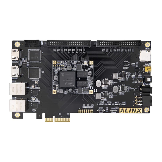
AX7103 User Manual Overview The ALINX ARTIX-7 FPGA Development board now released officially (module number: AX7103). In order to learn the FPGA board quickly, we write this manual for user. The ARTIX-7 FPGA development platform includes core board and expansion board, so that users can reuse the core board in their own projects conveniently. - Page 6 AX7103 User Manual 40针IO扩展口 40针IO扩展口 JTAG HDMI SiI9134 输出 QSPI SD Card 125Mhz FLASH HDMI SiI9013 CP2102 输入 UART DDR3 XILINX ARTIX-7 以太网 KSZ9031 FPGA 网口 DDR3 LED*4 以太网 KSZ9031 200Mhz 网口 核心板 按键*2 XADC接 PCIe x 4 口 Judge from the schematic diagram above, the AX7103 Development board could achieve the below functions.
- Page 7 AX7103 User Manual Reserved 2 pairs 2.54mm standard spacing 40-pin expansion header. They used to connect all kinds of AXSOC modules or outside circuit designed by users. There are 40pins for every expansion header, and one pin for 5V power supply, 2 pins for 3.3V power supply, 3 pins for ground, the other 34pins for IOs.
-
Page 8: Fpga Core Board
AX7103 User Manual FPGA Core Board 1. Overview AC7100 (module number of Core Board) core board, is a high performance core board using XILINX Artix-7 XC7A100T-2FGG484I chipset. Two DDR3 memories are connected to FPGA with 32bit data width and one 128Mbit QSPI FLASH is used for storage of FPGA bitstreams or application code. -
Page 9: Fpga
AX7103 User Manual AC7100 Bottom view 2. FPGA AC7100 Core board uses Xilinx Artix-7 FPGA device, the detail part number is XC7A100T-2FGG484I. Speed grade is 2, Temperature grade is industrial. The Xilinx Artix-7 FPGA ordering information is shown in Figure 2-2-1. Figure 2-2-1 Artix-7 Ordering Information Http://www.heijin.org 9 / 50... - Page 10 AX7103 User Manual Figure 2-2-1 FPGA chip The feature summary of XC7A100T is listed as below Items Parameters Logic Cells 101440 Slices 15850 CLB flip-flops 126800 Block RAM(kb) 4860 DSP Slices PCIe Gen2 XADC 1 is 12bit, 1Mbps AD GTP Transceiver 4,6.6Gb/s max Speed grade Temperature Grade...
-
Page 11: Differential Crystal Oscillator
AX7103 User Manual recommended power-off sequence is the reverse of the power-on. 3. Differential Crystal Oscillator AC7100 core board is equipped with two Sitime differential crystal oscillators , one is 200Mhz differential crystal oscillator for FPGA system clock, another is 148.5Mhz differential crystal oscillator for GTP transceiver reference. -
Page 12: Ddr3
AX7103 User Manual 2). 125Mhz Differential Clock The differential crystal oscillator marked as G2 in Figure 2-3-3, used to provide the reference input clock to GTP modules in FPGA. The Figure 2-3-3 is the circuit of 125Mhz clock for GPT transceiver. The output of differential crystal oscillator is connected to MGTREFCLK0P pin (F6) and MGTREFCLK0N pin (E6) of FPGA. - Page 13 AX7103 User Manual MT41K256M16HA-125. The DDR3 memory system connected to the memory connector of BANK 34 and BANK 35 in FPGA. Detail information of DDR3 SDRAM is shown in table 2-4-1 below Table 2-4-1 DDR3 SDRAM Configuration Part Capacity Vender U5,U6 MT41J256M16HA-125 256M x 16bit...
- Page 14 AX7103 User Manual Figure 2-4-2 DDR3 DRAM on board Pin Assignment of DDR3 DRAM: Net Name FPGA PIN Name FPGA P/N DDR3_DQS0_P IO_L3P_T0_DQS_AD5P_35 DDR3_DQS0_N IO_L3N_T0_DQS_AD5N_35 DDR3_DQS1_P IO_L9P_T1_DQS_AD7P_35 DDR3_DQS1_N IO_L9N_T1_DQS_AD7N_35 DDR3_DQS2_P IO_L15P_T2_DQS_35 DDR3_DQS2_N IO_L15N_T2_DQS_35 DDR3_DQS3_P IO_L21P_T3_DQS_35 DDR3_DQS3_N IO_L21N_T3_DQS_35 DDR3_DQ[0] IO_L2P_T0_AD12P_35 DDR3_DQ [1] IO_L5P_T0_AD13P_35 DDR3_DQ [2] IO_L1N_T0_AD4N_35...
- Page 15 AX7103 User Manual DDR3_DQ [10] IO_L8P_T1_AD14P_35 DDR3_DQ [11] IO_L10N_T1_AD15N_35 DDR3_DQ [12] IO_L7N_T1_AD6N_35 DDR3_DQ [13] IO_L10P_T1_AD15P_35 DDR3_DQ [14] IO_L7P_T1_AD6P_35 DDR3_DQ [15] IO_L12P_T1_MRCC_35 DDR3_DQ [16] IO_L18N_T2_35 DDR3_DQ [17] IO_L16P_T2_35 DDR3_DQ [18] IO_L14P_T2_SRCC_35 DDR3_DQ [19] IO_L17N_T2_35 DDR3_DQ [20] IO_L14N_T2_SRCC_35 DDR3_DQ [21] IO_L17P_T2_35 DDR3_DQ [22] IO_L13N_T2_MRCC_35 DDR3_DQ [23] IO_L18P_T2_35...
-
Page 16: Qspi Flash
AX7103 User Manual DDR3_A[14] IO_L6N_T0_VREF_34 DDR3_BA[0] IO_L9N_T1_DQS_34 DDR3_BA[1] IO_L9P_T1_DQS_34 DDR3_BA[2] IO_L11P_T1_SRCC_34 DDR3_S0 IO_L8P_T1_34 DDR3_RAS IO_L12P_T1_MRCC_34 DDR3_CAS IO_L12N_T1_MRCC_34 DDR3_WE IO_L7P_T1_34 DDR3_ODT IO_L14N_T2_SRCC_34 DDR3_RESET IO_L15P_T2_DQS_34 DDR3_CLK_P IO_L3P_T0_DQS_34 DDR3_CLK_N IO_L3N_T0_DQS_34 DDR3_CKE IO_L14P_T2_SRCC_34 5. QSPI Flash The board is assembled with 128Mbit of QSPI flash memory using an 4-bit data bus. -
Page 17: Led Light
AX7103 User Manual Net Name FPGA PIN Name FPGA P/N QSPI_CLK CCLK_0 QSPI_CS IO_L6P_T0_FCS_B_14 QSPI_DQ0 IO_L1P_T0_D00_MOSI_14 QSPI_DQ1 IO_L1N_T0_D01_DIN_14 QSPI_DQ2 IO_L2P_T0_D02_14 QSPI_DQ3 IO_L2N_T0_D03_14 Figure 2-5-2 shows onboard QSPI FLASH Figure 2-5-2 QSPI FLASH on board 6. LED light There are three RED LEDs on the FPGA, it includes power indicator LED, done indicator LED and user LED. -
Page 18: Reset Button
AX7103 User Manual Figure 2-6-2 LEDs on AC7100 board Pin Assignment of User LED Net Name FPGA PIN Name FPGA P/A Comments LED1 IO_L15N_T2_DQS_34 User LED Light 7. Reset Button AC7100 core board has a reset button, it is connected to the bank34 IO of FPGA. User can use this button to initialize the FPGA program. -
Page 19: Jtag Interface
AX7103 User Manual Pin Assignment of Reset Button Net Name FPGA PIN Name FPGA P/N Comment RESET_N IO_L17N_T2_34 Reset Button 8. JTAG Interface 。In the AC7100 core board, it reserves a JTAG interface (J1), it is used to download or debug FPGA program without expansion board. Figure 2-8-1 is circuit part of the JTAG port, only four JTAG signals (TMS, TDI, TDO, TCK) are connected to J1 for JTAG access Figure 2-8-1 JTAG interface schematic... -
Page 20: Board-To-Board Connector
AX7103 User Manual Figure 2-9-1MINI USB Port Schematic Figure 2-9-2 is mini USB port on AC7100 board Figure 2-9-2 MINI USB port on AC7100 board 10. Board-to-Board Connector The core board has four high-speed board-to-board connectors on PCB bottom side. Each connector is 80-pins of 0.5mm pin pitch, which is suitable for high-speed signal transmission. - Page 21 AX7103 User Manual the pin assignment of CON1 connector. 2-10-1 Table :Pin assignment of CN1 CON1 FPGA Voltage CON1 FPGA Voltage Name Level Name Level PIN1 VCCIN PIN2 VCCIN PIN3 VCCIN PIN4 VCCIN PIN5 VCCIN PIN6 VCCIN PIN7 VCCIN PIN8 VCCIN 地...
- Page 22 AX7103 User Manual PIN73 B16_L6_P 3.3V PIN74 PIN75 B16_L8_P 3.3V PIN76 PIN77 B16_L8_N 3.3V PIN78 PIN79 PIN80 Figure 2-10-1 is the CON1 connector on core board, and the pin1 of connector is marked on the board. Figure 2-10-1 CON Connector on board CON2 Connector The 80-Pin connector CON2 is used to extend the IOs of FPGA bank13 and bank14, the voltage level of these IOs are +3.3V standard.
- Page 23 AX7103 User Manual PIN37 B13_L8_P 3.3V PIN38 B14_L7_P 3.3V PIN39 Ground PIN40 Ground PIN41 B14_L11_N 3.3V PIN42 B14_L4_P 3.3V PIN43 B14_L11_P 3.3V PIN44 B14_L4_N 3.3V PIN45 B14_L14_N 3.3V PIN46 B14_L9_P 3.3V PIN47 B14_L14_P 3.3V PIN48 B14_L9_N 3.3V PIN49 Ground PIN50 Ground PIN51 B14_L5_N...
- Page 24 AX7103 User Manual CON3 FPGA Voltage CON3 FPGA Voltage Name Level Name Level PIN1 B15_IO0 3.3V PIN2 B15_IO25 3.3V PIN3 B16_IO0 3.3V PIN4 B16_IO25 3.3V PIN5 B15_L4_P 3.3V PIN6 B16_L21_N 3.3V PIN7 B15_L4_N 3.3V PIN8 B16_L21_P 3.3V PIN9 Ground PIN10 Ground PIN11 B15_L2_P...
- Page 25 AX7103 User Manual PIN77 FPGA_TCK 3.3V PIN78 FPGA_TDI 3.3V PIN79 FPGA_TDO 3.3V PIN80 FPGA_TMS 3.3V Figure 2-10-3 is the CON3 connector on core board, and the pin1 of connector is marked on the board. Figure 2-10-3 CON3 Connector on board Connector CON4 The 80-Pin connector CON4 is used to extend the IOs of FPGA bank16, high speed data of GTP transceivers and clock signals.
- Page 26 AX7103 User Manual Table 2-10-4:Pin Assignment of CON4 CON4 FPGA Voltage CON4 FPGA Voltage Name Level Name Level PIN1 PIN3 PIN5 PIN7 PIN9 Ground PIN10 Ground PIN11 PIN12 MGT_TX2_P Difference PIN13 PIN14 MGT_TX2_N Difference PIN15 PIN16 Ground PIN17 MGT_TX3_P Difference PIN18 MGT_RX2_P Difference...
-
Page 27: Power
AX7103 User Manual PIN75 B16_L19_P 3.3V PIN76 B16_L20_P 3.3V PIN77 B16_L19_N 3.3V PIN78 B16_L20_N 3.3V PIN79 PIN80 Figure 2-10-4 is the CON4 connector on core board, and the pin1 of connector is marked on the board. Figure 2-10-4 CON4 Connector on board Power The power supply voltage of the AC7100 core board is DC5V and can supply from mini USB port or board-to-board connector from expansion board. - Page 28 AX7103 User Manual TLV62130R 1.0V/3A Mini USB TLV62130R 1.8V/3A CON1 MGTAVTT TPS74801 MGTAVCC TPS74801 TLV62130R 1.5V/3A TPS51200 VREF 3.3V/3A TLV62130R SPX3819M5 VCCIO/0.5A -3-3 Figure2-11-1 Power design AC7100 core board uses the +5V power to generate +3.3V, +1.5V, +1.8V and +1.0V power output through the DC/DC power convertor. The output current of each power can be as high as 3A.
- Page 29 AX7103 User Manual MGTAVCC(+1.0V) FPGA GTP Transceivers, Bank216 There is requirement of power supply sequencing of Artix-7 FPGA, AC7100 core board is designed to meet it, the orders of power on for each power supply is as following: +1.0V -> +1.8V -> +1.5 V, +3.3V, VCCIO Power circuit on AC7100 core board is showed in Figure 2-11-2 below.
-
Page 30: Mechanical
AX7103 User Manual 12. Mechanical Top View Bottom View Http://www.heijin.org 30 / 50 30 / 50... -
Page 31: Expansion Board
AX7103 User Manual Expansion Board 1. Preview The following features are provided on the AX7102 expansion board: 1-channel PCIe x4 high speed data transmission Connector 2-channels 10/100M/1000M Ethernet RJ-45 Connector 1-channel HDMI Video Input Connector 1-channel HDMI Video Ouput Connector ... - Page 32 AX7103 User Manual When network connected to Gigabit Ethernet, data transmission between FPGA and PHY chip KSZ9031RNX by RGMII bus communication, transfer clock is 125Mhz, the data is sampled on the rising edged and the falling edged of clock. Figure 3-2-1 showed the connections between the FPGA, 2 Gigabit Ethernet PHY chips KSZ9031 E1_TXD[3:0]...
-
Page 33: Pcie X4 Connector
AX7103 User Manual The FPGA pins assignment to PHY1 as below: Net name FPGA Pin Comments E1_GTXC RGMII Transmit Clock E1_TXD0 RGMII Transmit Data bit0 E1_TXD1 RGMII Transmit Data bit1 E1_TXD2 RGMII Transmit Data bit2 E1_TXD3 RGMII Transmit Data bit3 E1_TXEN RGMII Transmit Enable E1_RXC... - Page 34 AX7103 User Manual The Transmit/ Receive signal of PCIe connectors connected to GTP transceiver of FPGA. 4 channels of TX signals and RX signals all connected to FPGA by differential signal methods. Single channel communication rate up to 5G bit bandwith.
-
Page 35: Hdmi Input Connector
AX7103 User Manual Negative PCIE_RX1_P PCIE channel 1 data receiver Positive PCIE_RX1_N PCIE channel 1 data receiver Negative PCIE_RX2_P PCIE channel 2 data receiver Positive PCIE_RX2_N PCIE channel 2 data receiver Negative PCIE_RX3_P PCIE channel 3 data receiver Positive PCIE_RX3_N PCIE channel 3 data receiver Negative PCIE_TX0_P PCIE channel 0 data Transmit Positive... - Page 36 AX7103 User Manual Figure 3-4-2 HDMI Output Connector on board FPGA Pin Assignment: Pins Name FPGA Pins 9134_nRESET 9134_CLK 9134_HS 9134_VS 9134_DE 9134_D[0] 9134_D[1] 9134_D[2] 9134_D[3] 9134_D[4] 9134_D[5] 9134_D[6] 9134_D[7] 9134_D[8] 9134_D[9] 9134_D[10] 9134_D[11] 9134_D[12] 9134_D[13] 9134_D[14] 9134_D[15] 9134_D[16] 9134_D[17] 9134_D[18] 9134_D[19] Http://www.heijin.org...
-
Page 37: Hdmi Input Connector
AX7103 User Manual 9134_D[20] 9134_D[21] 9134_D[22] 9134_D[23] 5. HDMI Input Connector The AX7103 used decoding chip SIL9013 HDMI of Silion Image company, supported input up to 1080P@60Hz, supported data output in various format. The IIC configure connector of SIL9013 connector to IOs of FPGA. To initialized and controlled the SIL9134 by FPGA program, HDMI Input connectors hardware designation as figure 3-5-1: SiI9013... -
Page 38: Sd Socket
AX7103 User Manual Figure 3-5-2 HDMI Input Connector on board FPGA pins assignment: Pin Name FPGA Pins 9013_nRESET 9013_CLK 9013_HS 9013_VS 9013_DE 9013_D[0] 9013_D[1] 9013_D[2] 9013_D[3] 9013_D[4] 9013_D[5] 9013_D[6] 9013_D[7] 9013_D[8] 9013_D[9] 9013_D[10] 9013_D[11] 9013_D[12] 9013_D[13] 9013_D[14] 9013_D[15] 9013_D[16] 9013_D[17] 9013_D[18] 9013_D[19] 9013_D[20]... -
Page 39: Usb Serial Port
AX7103 User Manual +3.3V +3.3V FPGA Artix-7 Figure 3-6-1 Design of SD Interface Figure 3-6-2 shows the SD card socket on board. Figure 3-6-2 SD card socket on board Pin Assignment of SD Socket SD Mode Net Name FPGA PIN SD_CLK AB12 SD_CMD... - Page 40 AX7103 User Manual board can communicate with PC for UART communication. The hardware design of USB UART is showed as Figure 3-7-1. Micro USB UART1_TXD FPGA VBUS REGIN CP2102 UART1_RXD D+/- 3-7-1 USB UART Interface Figure 3-7-2 below shows the USB UART onboard. 3-7-2 USB UART onboard There are two LEDs on board to indicate the UART operation status, the LED3 is used to indicate receiving status, and the LED4 is used to indicate sending status.
-
Page 41: Eeprom 24Lc04
AX7103 User Manual 3-7-3 USB USB UART LED Indication PIN Assignment of USB UART.: Net Name FPGA PIN UART1_RXD UART1_TXD 8. EEPROM 24LC04 The AX7103 used on chip of EEPROM, model 24LC04, Capacity of 4Kbit(2*256*8bit)comprise 2 blocks of 256byte, communication by IIC bus. EEPROM on board is to use to study IIC bus communication method. -
Page 42: Gpio Expansion Headers
AX7103 User Manual EEPROM_I2C_SDA 9. GPIO Expansion Headers The expansion board reserved 2 pairs 2.54mm standard spacing 40-pin expansion header. They used to connect all kinds of AXSOC modules or outside circuit designed by users. There are 40pins for every expansion header, and one pin for 5V power supply, 2 pins for 3.3V power supply, 3 pins for ground, the other 34pins for IOs. - Page 43 AX7103 User Manual J11 Pin FPGA PIN J11 Pin FPGA PIN AB10 AA10 AA11 AA15 AB15 AA16 AB16 AB17 +3.3V +3.3V Figure 3-9-3 below shows the circuit schematic of expansion header (J13). Http://www.heijin.org 43 / 50 43 / 50...
- Page 44 AX7103 User Manual Figure 3-9-3 Expansion header J13 schematic Below picture is the J13on board. Pin 1 and Pin2 marked on board. Figure 3-9-2 expansion header J13 on board Pin Assignment of expansion header J13 J13 PIN FPGA PIN J13 PIN FPGA PIN AB21 AB22...
-
Page 45: Jtag Connector
AX7103 User Manual AA18 AB18 +3.3V +3.3V 10. JTAG Connector The AX7103 Board reserves a 10Pin JTAG interface for downloading programs to FPGA QSPI FLASH. Each pin of JTAG interface on the expansion headers is connected to two diodes and a resistor that provides protection against high and low voltages. -
Page 46: Xadc Connector(Not Install By Default
AX7103 User Manual Figure 3-10-2 JTAG connector on board 11. XADC Connector(Not install by default) AX7103 expansion board expanded XADC connector interface, the connectors used a 2x8 2.54mm pitch double-row pin. The XADC connectors expanded 3 pairs of ADC differential input connector, connected to 12-Bit 1Msps Analog to Digital Converter of FPGA. -
Page 47: Buttons
AX7103 User Manual Figure 3-11-3 XADC on expansion board Pin Assignment of XADC Connectors XADC FPGA Input Description Connectors magnitude VP_0 : Peak-to-Peak FPGA 1,2 dedicated VN_0 : XADC input channel AD9P : Peak-to-Peak FPGA assisted 5,6 XADC input AD9N : channel (could use as normal IO)... -
Page 48: Led
AX7103 User Manual 3.3V KEY1 FPGA KEY2 Figure 3-12-1 button hardware design schematic Figure 3-12-2 are 2 user buttons on expansion board Figure 3-12-2 2 user buttons on expansion board Pin Assignment of Buttons.: Net Name FPGA PIN KEY1 KEY2 13. -
Page 49: Power Supply
AX7103 User Manual 3.3V LED1 LED2 LED3 LED4 FPGA Figure 3-13-1 LED hardware design schematic Figure 3-14-2 is the two user LEDs on expansion board Figure 3-13-2 User LEDs on expansion board Pin Assignment of User LEDs: Net Name FPGA PIN LED1 LED2 LED3... - Page 50 AX7103 User Manual Figure 3-14-1 Power Schematic on expansion board Figure 3-14-2 shows the DC/DC circuit on board 图3-14-2 DC/DC circuit on expansion board Http://www.heijin.org 50 / 50 50 / 50...
Need help?
Do you have a question about the AX7103 FPGA and is the answer not in the manual?
Questions and answers