
Related Manuals for ADLINK Technology AMD COM Express Express-VR7


Summary of Contents for ADLINK Technology AMD COM Express Express-VR7
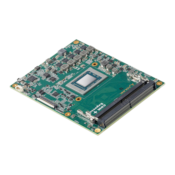
- Page 1 Express-VR7 User’s Guide PICMG COM.0 R3.1 Express-VR7 User’s Guide Revision: 0.1 Preliminary Date: 2024-05-16 Part Number: 50M-72140-1000 Page 1 Copyright © 2024 ADLINK Technology, Inc.
-
Page 2: Revision History
Express-VR7 User’s Guide PICMG COM.0 R3.1 Revision History Revision Description Date Author Preliminary release 2024-05-16 Page 2 Copyright © 2024 ADLINK Technology, Inc. -
Page 3: Preface
Product names mentioned herein are used for identification purposes only and may be trademarks / registered trademarks of respective companies. Copyright © 2024 ADLINK Technology Incorporated This document contains proprietary information protected by copyright. All rights are reserved. No part of this manual may be reproduced by any mechanical, electronic, or other means in any form without prior written permission of the manufacturer. - Page 4 Only install/attach and operate equipment on stable surfaces and/or recommended mountings; • If the equipment will not be used for long periods of time, turn off the power source and unplug the equipment. • Page 4 Copyright © 2024 ADLINK Technology, Inc.
- Page 5 Caution: This information indicates the possibility of minor physical injury, component damage, data loss, and/or program corruption. Warning: This information warns of possible serious physical injury, component damage, data loss, and/or program corruption. Page 5 Copyright © 2024 ADLINK Technology, Inc.
- Page 6 ADLINK Technology GmbH Hans-Thoma-Strasse 11, D-68163 Mannheim, Germany Tel: +49-621-43214-0 Fax: +49-621 43214-30 Email: emea@adlinktech.com Please visit the Contact page at www.adlinktech.com for information on how to contact the ADLINK regional office nearest you. Page 6 Copyright © 2024 ADLINK Technology, Inc.
-
Page 7: Table Of Contents
Gigabit Ethernet................................................................. 27 4.3.3 SATA ....................................................................28 4.3.4 PCI Express ................................................................... 29 4.3.5 LPC Bus ..................................................................33 4.3.6 USB ....................................................................34 4.3.7 SPI Bus (BIOS only) ..............................................................35 4.3.8 Miscellaneous ................................................................36 Page 7 Copyright © 2024 ADLINK Technology, Inc. - Page 8 8.3. Module Dimensions – Side View ............................................................ 63 8.4. Height of Processor and Static Compressive Load ....................................................63 Thermal Solutions ................................................................. 64 8.5.1 HTS-B ..................................................................... 64 8.5.2 HTS-BT ................................................................... 65 8.5.3 THS-B ..................................................................... 66 Page 8 Copyright © 2024 ADLINK Technology, Inc.
- Page 9 8.5.4 THS-BT ................................................................... 67 8.5.5 THSF-B ................................................................... 68 8.5.6 THSH-B ..................................................................69 8.6. Board to Board Connectors............................................................... 70 8.7. Mounting Method ................................................................. 72 8.8. Standoff Types ..................................................................73 8.9. Installation ....................................................................74 Page 9 Copyright © 2024 ADLINK Technology, Inc.
-
Page 10: List Of Figures
Figure 1 – Module functional block diagram ..................................................19 Figure 2 - Module rear side row and pin numbering ..............................................20 Figure 3 – Module feature locations ....................................................... 52 Figure 4 – Express-VR7 and Debug Module ..................................................53 Page 10 Copyright © 2024 ADLINK Technology, Inc. -
Page 11: Introduction
Additional General Purpose SPI (GP_SPI) and remoted management dedicated IPMB are offered by project basis. Support for SMBus and I2C is also provided. The module is equipped with SPI AMI EFI BIOS with CMOS backup, supporting embedded features such as remote console, hardware monitor, and watchdog timer. Page 11 Copyright © 2024 ADLINK Technology, Inc. -
Page 12: Specifications
Up to 64GB DDR5, dual memory channel in 2x SODIMM sockets, maximum 32GB per socket, ECC or non-ECC Up to 4800 MT/s memory speed (dependent on SKUs) 2x SODIMM sockets on top side Cache (L3) 16MB: V3C48, V3C18I, V3C18, V3C16 8MB: V3C44, V3C14 Page 12 Copyright © 2024 ADLINK Technology, Inc. -
Page 13: Expansion Buses
C from CPU is supported by BOM option and project basis SMBus from EC (embedded controller) is supported by BOM option and project basis Additional GP_SPI (general purpose SPI by project basis) Page 13 Copyright © 2024 ADLINK Technology, Inc. -
Page 14: Kr Ethernet
Optical Fiber/Copper PHY and firmware. (2) Additional MDC/MDIO is offered for specific use case based on 10GBASE-T, by project basis. (3) SGMII offering for specific use case and by project basis. (TBC) (4) 10G_SDP support is by project basis Page 14 Copyright © 2024 ADLINK Technology, Inc. -
Page 15: Gbe Ethernet
Console Redirection COM 1 or COM 2 selectable in BIOS SER0, SER1 from CPU UART are supported by BOM option and project basis Up to 4 serial ports supported by standard BIOS, including Super I/O on carrier board Page 15 Copyright © 2024 ADLINK Technology, Inc. -
Page 16: Trusted Platform Module (Tpm)
2.7. SEMA Board Controller Supports: Voltage/current monitoring, power sequence debug support, AT/ATX mode control, logistics and forensic information, flat panel control, general purpose I2C, failsafe BIOS (dual BIOS, opt. support), watchdog timer and fan control Page 16 Copyright © 2024 ADLINK Technology, Inc. -
Page 17: Ipmb (Intelligent Platform Management Bus)
Power States: C0-C3, S0, S5, S5 ECO mode (Wake-on-USB S3, WoL S3/S5) ECO Mode support for deep S5 for 5Vsb power saving Power Consumption Please contact your ADLINK representative for the document “COM Express Module Power Consumption”. Page 17 Copyright © 2024 ADLINK Technology, Inc. -
Page 18: Mechanical And Environmental
Shock and Vibration IEC 60068-2-64 and IEC-60068-2-27 MIL-STD-202F, Method 213B, Table 213-I, Condition A and Method 214A, Table 214-I, Condition D HALT tested Thermal Stress, Vibration Stress, Thermal Shock and Combined Test Page 18 Copyright © 2024 ADLINK Technology, Inc. -
Page 19: Block Diagram
4x GPO eSPI 4x GPO eSPI to LPC Bridge IC DDR5 SODIMM Thermal sensor ECC/non-ECC (TBC) Embedded Controller DDR5 SODIMM IPMB Thermal sensor ECC/non-ECC (board) LPC/eSPI Figure 1 – Module functional block diagram Page 19 Copyright © 2024 ADLINK Technology, Inc. -
Page 20: Pinout And Signal Descriptions
COM.0 R3.1 specification. Signals described in the specification but not supported on the Express-VR7 are strikethrough STRIKETHROUGH A110 Figure 2 - Module rear side row and pin numbering Note: The 2x SO-DIMM sockets (grey color) are located on top side. Page 20 Copyright © 2024 ADLINK Technology, Inc. - Page 21 10G_KR_RX2- 10G_KR_TX2- GND (fixed) GND (fixed) GND (fixed) GND (fixed) IPMB_CLK* SPKR RSVD10G RSVD10G / GP_SPI_CLK* IPMB_DAT* I2C_CK RSVD10G RSVD10G / GP_SPI_MOSI* BIOS_DIS0# I2C_DAT RSVD10G RSVD10G / GP_SPI_MISO* THRMTRIP# THRM# CEI_RST# CEI_PRSNT# Page 21 Copyright © 2024 ADLINK Technology, Inc.
- Page 22 PCIE_RX19- PCIE_TX19- GPI1 GPO3 PCIE_TX1+ PCIE_RX1+ PCIE_TX1- PCIE_RX1- PCIE_RX20+ PCIE_TX20+ WAKE0# PCIE_RX20- PCIE_TX20- GPI2 WAKE1# RAPID_SHUTDOWN PCIE_TX0+ PCIE_RX0+ PCIE_RX21+ PCIE_TX21+ PCIE_TX0- PCIE_RX0- PCIE_RX21- PCIE_TX21- GND (fixed) GND (fixed) GND (fixed) GND (fixed) Page 22 Copyright © 2024 ADLINK Technology, Inc.
- Page 23 D101 PCIE_TX31+ A102 SER1_RX B102 FAN_TACHIN C102 PCIE_RX31- D102 PCIE_TX31- A103 LID# B103 SLEEP# C103 D103 A104 VCC_12V B104 VCC_12V C104 VCC_12V D104 VCC_12V A105 VCC_12V B105 VCC_12V C105 VCC_12V D105 VCC_12V Page 23 Copyright © 2024 ADLINK Technology, Inc.
- Page 24 3. Features listed below are supported by project basis (1) IPMB function (2) GBE0_SDP with specific LAN controller (3) 10G_SDP 0-3. (4) GP_SPI, general purpose SPI. (5) Additional MDC/MDIO (10G_PHY_MDC_SCL1, 10G_PHY_MDIO_SDA1). All these project basis support features are still in development stage. Page 24 Copyright © 2024 ADLINK Technology, Inc.
-
Page 25: Signal Terminology Descriptions
Pull-down strap. A Module output pin that is either tied to GND or is not connected. Used to signal Module capabilities to the Carrier Board. PU (pull-up) resistor on module PD (pull-down) resistor on module Page 25 Copyright © 2024 ADLINK Technology, Inc. -
Page 26: Ab Connector Signal Descriptions
Transmit enable I 3.3VSB PD 10K Not supported NCSI_RX_ER Receive error Not supported 3.3VSB Network Controller hardware arbitration input I 3.3VSB Not supported NCSI_ARB_IN Network Controller hardware arbitration output Not supported NCSI_ARB_OUT 3.3VSB Page 26 Copyright © 2024 ADLINK Technology, Inc. -
Page 27: Gigabit Ethernet
Gigabit Ethernet Controller 0 Software-Definable Pin. Can also be used for GBE0_SDP IO 3.3VSB of LAN controller, project IEEE1588 support such as 1pps signal. basis Note: GBE0_ACT# and GBE0_LINK# share the same pin from LAN controller. Page 27 Copyright © 2024 ADLINK Technology, Inc. -
Page 28: Sata
SATA1_RX- (S)ATA_ACT# ATA (parallel and serial) or SAS activity indicator, active low. O 3.3V PU 10K 3.3V 4.3.3.1. I/O Assignments Name Physical Lane on CPU Comment SATA0 Lane 10 SATA1 Lane 11 Page 28 Copyright © 2024 ADLINK Technology, Inc. -
Page 29: Pci Express
O PCIE Not supported PCIE_TX8- PCIE_RX8+ PCI Express channel 8, Receive Input differential pair. I PCIE Not supported PCIE_RX8- PCIE_TX9+ PCI Express channel 9, Transmit Output differential pair. O PCIE Not supported PCIE_TX9- Page 29 Copyright © 2024 ADLINK Technology, Inc. - Page 30 PCI Express Reference Clock output for all PCI Express and PCI O PCIE PCIE_CLK_REF- Express Graphics Lanes. PCIE_CLK_REF1+ Second reference clock output for higher speed PCI Express O PCIE PCIE_CLK_REF1- implementation on Lanes 16 to 31, for Type 7 implementations only Page 30 Copyright © 2024 ADLINK Technology, Inc.
- Page 31 PCI Express lane configuration as below Note: PCIe Lane 1, 2, 3 can be used as x1 but requires prior inquiries. PCIe Lane 2-3 can be used as one x2 but requires prior inquiries Page 31 Copyright © 2024 ADLINK Technology, Inc.
- Page 32 Lane 15 PCIE4 Lane 16 PCIE5 Lane 17 PCIE16 Lane 7 PCIE17 Lane 6 PCIE18 Lane 5 PCIE19 Lane 4 PCIE20 Lane 3 PCIE21 Lane 2 PCIE22 Lane 1 PCIE23 Lane 0 Page 32 Copyright © 2024 ADLINK Technology, Inc.
-
Page 33: Lpc Bus
LPC serial DMA request I 3.3V Not supported LPC_DRQ1# LPC_SERIRQ LPC serial interrupt I/O 3.3VSB PU 8.2K 3.3VSB LPC_CLK LPC clock output –33MHz nominal O 3.3VSB The LPC_CLK frequency is 24MHz on this platform Page 33 Copyright © 2024 ADLINK Technology, Inc. -
Page 34: Usb
USB0. A high value indicates that a host is present. *Note: A pull-up for this line shall be present on the module. An open drain driver from a USB current monitor on the carrier board may drive this line low. Page 34 Copyright © 2024 ADLINK Technology, Inc. -
Page 35: Spi Bus (Bios Only)
PU 10K Carrier shall pull to GND or leave not connected. 3.3VSB BIOS_DIS1# Selection strap to determine the BIOS boot device. PU 10K Carrier shall pull to GND or leave not connected 3.3VSB Page 35 Copyright © 2024 ADLINK Technology, Inc. -
Page 36: Miscellaneous
PD only when TPM on module. Active high. TPM chip has an internal pull down. This Modules implementing a TPM shall pull down signal is used to indicate Physical Presence to the TPM. Not Supported Page 36 Copyright © 2024 ADLINK Technology, Inc. -
Page 37: Smbus
General purpose I²C port data I/O line I/O OD PU 2.2K 3.3VSB 3.3VSB Note: I2C source from EC is default setting. I2C source from SoC’s I2C is by build option supported by project basis. Page 37 Copyright © 2024 ADLINK Technology, Inc. -
Page 38: General Purpose I/O (Gpio)
O CMOS Power rail tolerance 5V, 12V 3.3V There shall be PD on carrier board SER1_RX A102 General purpose serial port receiver I CMOS PU 10K 3.3V Power rail tolerance 5V, 12V 3.3V Page 38 Copyright © 2024 ADLINK Technology, Inc. -
Page 39: Ipmb (Optional)
3.3VSB 3.3VSB located on the Carrier. Note: IPMB via a Module MMC is supported by project basis and it is still in development (TBC) Page 39 Copyright © 2024 ADLINK Technology, Inc. -
Page 40: Power And System Management
I OD 3.3VSB SLEEP# B103 Sleep button. Low active signal used by the ACPI operating system to bring the I OD 3.3VSB system to sleep state or to wake it up again. Page 40 Copyright © 2024 ADLINK Technology, Inc. - Page 41 USB devices that are to be powered in the S5 / S4 / S3 Suspend states should not RSMRST_OUT O CMOS have their 5V VBUS power enabled before RSMRST_OUT# transitions to the hi 3.3VSB state. Page 41 Copyright © 2024 ADLINK Technology, Inc.
-
Page 42: Power And Ground
A51, A57, A60, A66, A70, A73, path. A76, A79, A80, A83, A87, A90, A100, A110, B1, B11, B21, B28, B31, B38, B41, B51, B60, B70, B73, B76, B79, B80, B83, B90, B100, B110 Page 42 Copyright © 2024 ADLINK Technology, Inc. -
Page 43: Cd Connector Signal Descriptions
I PCIE AC coupled off module USB_SSRX3+ data path on USB3 USB_SSTX3- Additional Transmit signal differential pairs for the SuperSpeed O PCIE AC coupled on module USB_SSTX3+ USB data path on USB3 Page 43 Copyright © 2024 ADLINK Technology, Inc. -
Page 44: Pci Express
I PCIE Not supported PCIE_RX6- PCIE_TX7+ PCI Express channel 7, Transmit Output differential pair. O PCIE Not supported PCIE_TX7- PCIE_RX7+ PCI Express channel 7, Receive Input differential pair. I PCIE Not supported PCIE_RX7- Page 44 Copyright © 2024 ADLINK Technology, Inc. -
Page 45: Kr Ethernet
3.3VSB development stage CEI_MDC MDIO clock - for PHY setup O 3.3VSB PU 1K TBD, it will be fine tune during 3.3VSB development stage 10G_SDP0 Software-Definable Pins I/O 3.3VSB 10G_SDP1 10G_SDP2 10G_SDP3 Page 45 Copyright © 2024 ADLINK Technology, Inc. - Page 46 Optical Fiber/Copper PHY and firmware. (2) Additional MDC/MDIO is offered for specific use case based on 10GBASE-T, by project basis. (3) SGMII offering for specific use case and by project basis. (4) 10G_SDP support is by project basis. Page 46 Copyright © 2024 ADLINK Technology, Inc.
-
Page 47: Pci Express
PCIE_TX23+ PCI Express channel 23, Transmit Output differential pair. O PCIE AC coupled on Module PCIE_TX23- PCIE_RX23+ PCI Express channel 23, Receive Input differential pair. I PCIE AC coupled off Module PCIE_RX23- Page 47 Copyright © 2024 ADLINK Technology, Inc. - Page 48 PCIE_RX31+ C101 PCI Express channel 31, Receive Input differential pair. I PCIE Not supported PCIE_RX31- C102 Note: Both of PCIE_CLK_REF1 and PCIE_CLK_REF can be used for PCIe lane 16-23 but PCIE_CLK_REF1 preferred. Page 48 Copyright © 2024 ADLINK Technology, Inc.
-
Page 49: Gp_Spi
Data out from Module SPI Master to Carrier SPI Slave O 3.3VSB “Master Out Slave In” GP_SPI_CLK Clock from Module SPI Master to Carrier SPI Slave O 3.3VSB Note: GP_SPI supported by project basis Page 49 Copyright © 2024 ADLINK Technology, Inc. -
Page 50: Module Type Definition
Carrier Board logic may also implement a fault indicator such as an LED. TYPE10# In case of a type 10 module this pin signal is tied to GND through a 47K resistor No PD on the module. Page 50 Copyright © 2024 ADLINK Technology, Inc. -
Page 51: Power And Ground
C103, C110, D1, D2, D5, D8, D11, D14, D18, D21, D25, D28, D31, D41, D44, D48, D51, D54, D60, D63, D64, D67, D70, D73, D76, D77, D80, D83, D84, D87, D90, D93, D96, D97, D100, D103, D110 Page 51 Copyright © 2024 ADLINK Technology, Inc. -
Page 52: Additional Features
This chapter describes connectors, LEDs, switches and additional items located on the module and not necessarily included in the PICMG standard spec- ification. The locations of these items are shown below: 40-pin Debug Status Connector LEDs BIOS Default Reset Button BIOS Boot Select Figure 3 – Module feature locations Page 52 Copyright © 2024 ADLINK Technology, Inc. -
Page 53: Debug Connector
I2C bus for BIOS POST code readout SPI BIOS programming interface Embedded Controller programming interface The debug board for Express-VR7 usage is DB40-HPC Figure 4 – Express-VR7 and Debug Module Page 53 Copyright © 2024 ADLINK Technology, Inc. -
Page 54: Status Leds
Rebooted after PWRBTN WD LED = LED OFF Rebooted after RESET BTN WD LED = LED OFF Note: Only a RESET not initiated by the BMC can clear the WD LED (user action) Page 54 Copyright © 2024 ADLINK Technology, Inc. -
Page 55: Exception Codes
Express-VR7 User’s Guide PICMG COM.0 R3.1 5.3. Exception Codes Exception Code Error Message NOERROR NO_SLP_S5 NO_SLP_S4 NO_SLP_S3 BIOS_FAIL RESET_FAIL NO_CB_PWROK CRITICAL_TEMP POWER_FAIL VOLTAGE_FAIL RSMRST_FAIL NO_VDDQ_PG NO_VCORE_PG NO_SYS_GD NO_V3P3A NO_PWRSRC_GD Page 55 Copyright © 2024 ADLINK Technology, Inc. -
Page 56: Fan Connector
Express-VR7 User’s Guide PICMG COM.0 R3.1 5.4. Fan Connector Connector type: JVE 24W1125A-04M00 4 3 2 1 Name Description FAN_PWMOUT FAN_TACHIN Page 56 Copyright © 2024 ADLINK Technology, Inc. -
Page 57: Bios Default Reset Button
2. Keep the BIOS Setup Defaults Reset Button pressed and boot up the system. You can release the button when the BIOS prompt screen appears 3. The BIOS prompt screen will display a confirmation that BIOS defaults have been reset and request that you reboot the system. Page 57 Copyright © 2024 ADLINK Technology, Inc. -
Page 58: Bios Boot Select
In either mode, BIOS Select and Mode Configuration Switch Pin 1 is used to select whether to boot from SPI0 or SPI1. Mode Pin 1 Pin 2 Boot from SPI0 (default) Boot from SPI1 Set BIOS to PICMG mode (default) Set BIOS to Failsafe BIOS mode Page 58 Copyright © 2024 ADLINK Technology, Inc. -
Page 59: Bios Checkpoints, Beep Codes
These PCI add-on cards show the value of I/O port 80h on an LED display. Aptio V Checkpoint and Beep Codes Download the Aptio V Checkpoint and Beep Codes from the AMI website at: www.ami.com/download/aptio-v-checkpoint-and-beep-codes Page 59 Copyright © 2024 ADLINK Technology, Inc. -
Page 60: Software Support
Express-VR7 User’s Guide PICMG COM.0 R3.1 7. Software Support 7.1. Yocto Linux https://github.com/ADLINK/meta-adlink-amd 7.2. Ubuntu 20.04.3 LTS 7.3. SEMA API Page 60 Copyright © 2024 ADLINK Technology, Inc. -
Page 61: Mechanical And Thermal
Express-VR7 User’s Guide PICMG COM.0 R3.1 8. Mechanical and Thermal All dimensions are shown in mm with a tolerance of +/- 0.25mm unless otherwise noted. 8.1. Module Dimensions – Top View Page 61 Copyright © 2024 ADLINK Technology, Inc. -
Page 62: Module Dimensions - Bottom View
Express-VR7 User’s Guide PICMG COM.0 R3.1 8.2. Module Dimensions – Bottom View Page 62 Copyright © 2024 ADLINK Technology, Inc. -
Page 63: Module Dimensions - Side View
Tolerance Module PCB 1.28 mm +/- 0.1mm Static Compressive Load Another key factor to consider is the static compressive load. The Express-VR7 module exhibits a processor maximum pressure die of 40 lbf. Page 63 Copyright © 2024 ADLINK Technology, Inc. -
Page 64: Thermal Solutions
Express-VR7 User’s Guide PICMG COM.0 R3.1 8.5. Thermal Solutions 8.5.1 HTS-B Page 64 Copyright © 2024 ADLINK Technology, Inc. -
Page 65: Hts-Bt
Express-VR7 User’s Guide PICMG COM.0 R3.1 8.5.2 HTS-BT Page 65 Copyright © 2024 ADLINK Technology, Inc. -
Page 66: Ths-B
Express-VR7 User’s Guide PICMG COM.0 R3.1 8.5.3 THS-B Page 66 Copyright © 2024 ADLINK Technology, Inc. -
Page 67: Ths-Bt
Express-VR7 User’s Guide PICMG COM.0 R3.1 8.5.4 THS-BT Page 67 Copyright © 2024 ADLINK Technology, Inc. -
Page 68: Thsf-B
Express-VR7 User’s Guide PICMG COM.0 R3.1 8.5.5 THSF-B Page 68 Copyright © 2024 ADLINK Technology, Inc. -
Page 69: Thsh-B
Express-VR7 User’s Guide PICMG COM.0 R3.1 8.5.6 THSH-B Page 69 Copyright © 2024 ADLINK Technology, Inc. -
Page 70: Board To Board Connectors
401-55101-51, ept 401-55103-51 Foxconn QT002206-4141-3H, Foxconn QT5GB26-74703-3H 220-pin board-to-board connector with 0.5mm for a stacking height of 8 mm. • This connector can be used with 8-mm through-hole standoffs (SMT type). • Page 70 Copyright © 2024 ADLINK Technology, Inc. - Page 71 Rated voltage: 50V AC • Insulation resistance: 100M or greater @ 500 VDC • Temperature rating: -40°C to 85°C • UL certification (ECBT2.E28476) • Copper alloy (contacts) • Housing: thermo-plastic molded compound (L.C.P.) • Page 71 Copyright © 2024 ADLINK Technology, Inc.
-
Page 72: Mounting Method
9 mm through-hole standoffs Carrier Board ~ 2 mm COM Express Module ~ 2 mm 8 mm threaded standoff (DIP) M2.5 : 16 mm with spring / washer Carrier Board ~ 2 mm Page 72 Copyright © 2024 ADLINK Technology, Inc. -
Page 73: Standoff Types
SMT type. Other types not listed are available upon request. 5mm through-hole standoff (SMT type) 5mm threaded standoff (DIP type) P/N: 33-72000-0050 P/N: 33-72016-0050 8mm through-hole standoff (SMT type) 8mm threaded standoff (DIP type) P/N: 33-72000-0080 P/N: 33-72015-0050 Page 73 Copyright © 2024 ADLINK Technology, Inc. -
Page 74: Installation
1. Before mounting the heatsink, install the required memory modules onto the SODIMM socket(s) on the COM Express module. 2. Remove the protective membranes from the thermal pads. All thermal pads have a protective membrane (module dependent) Page 74 Copyright © 2024 ADLINK Technology, Inc. - Page 75 4. Place the COM Express module and heatsink assembly onto the connectors on the carrier board as exemplified below. Then press down on the module until it is firmly seated on the carrier board. Page 75 Copyright © 2024 ADLINK Technology, Inc.
- Page 76 5. Use the 5x M2.5, L=16mm screws provided to secure the COM Express module to the carrier board from the solder side. 6. If you are installing a heatsink with a fan, plug the fan connector into the carrier board as shown. Page 76 Copyright © 2024 ADLINK Technology, Inc.
Need help?
Do you have a question about the AMD COM Express Express-VR7 and is the answer not in the manual?
Questions and answers