
Subscribe to Our Youtube Channel
Related Manuals for ADLINK Technology Express-BASE


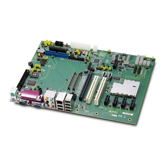
Summary of Contents for ADLINK Technology Express-BASE
- Page 1 Express-BASE User’s Manual Manual Revision: 2.30 Revision Date: July 6, 2011 Part Number: 50-1J012-1030...
- Page 2 (compatible with PICMG COM Express Carrier Design Guide) 2.30 2011/07/06 Updated to D2 PCB version: Removed TV-out, extended power connectors; added LVDS panel control header and jumpers, SPI BIOS socket and Secondary BIOS instructions, ATX 12V 4-pin connector, ATX power connector info Page 2 Express-BASE User’s Manual...
-
Page 3: Table Of Contents
LVDS Jumper Settings ......................25 6.13 Keyboard & Mouse ......................26 6.14 Serial and IrDA Ports ......................26 6.15 Parallel Port ........................27 6.16 Storage: SATA, PATA, FDD, CF ..................27 6.18 Power Connectors ......................30 Express-BASE User’s Manual Page 3... - Page 4 POST & Module Type Display ..................... 39 Indicator LEDs ........................40 Digital I/O LEDs ........................40 ATX Power Connectors ....................... 41 AT Power Mode ........................42 Important Safety Instructions ..................43 Getting Service ......................44 Page 4 Express-BASE User’s Manual...
-
Page 5: Preface
Preface Copyright 2006-2011 ADLINK Technology, Inc. This document contains proprietary information protected by copyright. All rights are reserved. No part of this manual may be reproduced by any mechanical, electronic, or other means in any form without prior written permission of the manufacturer. - Page 6 Information to prevent minor physical injury, component damage, data loss, and/or program corruption when trying to complete a task. Information to prevent serious physical injury, component damage, data loss, and/or program corruption when trying to complete a specific task. Page 6 Express-BASE User’s Manual...
-
Page 7: Introduction
OEM board. Express-BASE is a standard ATX size carrier board. Together with the COM Express module of your choice and off the shelf add-on cards you can quickly emulate the functionality of your desired end product for software development and hardware verification. -
Page 8: Special Features
COM Express modules do not have a Super I/O chip onboard as this is considered legacy. Therefore, a Super I/O is placed on the carrier board as an optional item. The Express-BASE uses a Winbond W83627HG-AW that supports FDD, LPT, COM and PS/2 Keyboard and Mouse. -
Page 9: Component Location
CNY1 PCIE7 CN32 CN42 CN21 JPY11 JPZ3 CN13 CN20 CNZ1 CNY5 JPZ2 JPZ1 CNY8 JPZ4 CNY4 CN41 JPY10 CN15 CNY9 CN35 JPA1 CN14 CN10 JPY8 CNZ2 CN33 JPY1 CN26 SW3 SW1 CN37 CN19 CN18 CN24 Express-BASE User’s Manual Page 9... -
Page 10: Function Block Diagram
ALC888 Audio on Codec Rear I/O Gigabit Onboard IDE Ethernet PATA Connector Rear I/O CRT VGA Rear I/O LVDS headers PCI Express 32-bit PCI Express Card 6x USB on Rear I/O 1x USB on header Page 10 Express-BASE User’s Manual... -
Page 11: Mechanical Dimensions
5 Mechanical Dimensions tolerances ± 0.05 mm Other tolerances ± 0.2 mm Express-BASE User’s Manual Page 11... -
Page 12: Connectors And Pin-Outs
COM.0 - COM Express Module Base specification, Revision 2”. This document includes: description of pinouts, signal descriptions and mechanical characteristics of the COM Express specification. The Express-BASE is compatible with COM Express modules in Basic and Compact form factor, Type 2 pinout, COM.0 Rev. 1.0 and Rev. 2.0. -
Page 13: Com Express Board-To-Board Connectors
GND (FIXED) GND (FIXED) GND (FIXED) USB2- USB3- PCI_AD21 PCI_AD24 USB2+ USB3+ PCI_AD23 PCI_AD26 USB_2_3_OC# USB_0_1_OC# PCI_C/BE3# PCI_AD28 USB0- USB1- PCI_AD25 PCI_AD30 Pin definitions that are new for COM.0 Rev. 2.0 are highlighted in bold. Express-BASE User’s Manual Page 13... - Page 14 D108 VCC_12V A109 VCC_12V B109 VCC_12V C109 VCC_12V D109 VCC_12V A110 GND (FIXED) B110 GND (FIXED) C110 GND (FIXED) D110 GND (FIXED) Pin definitions that are new for COM.0 Rev. 2.0 are highlighted in bold. Page 14 Express-BASE User’s Manual...
-
Page 15: Pci Express And Pci Express Graphic (Peg) Slots
PERST# REFCLK+ PETp0 REFCLK- PETn0 PERp0 PERn0 CN44: ExpressCard (PCIE3, USB7) Signal Signal +3.3V USBD- +3.3V USBD+ CLKREQ# CPUSB# CPPE# RESERVED REFCLK- RESERVED REFCLK+ SMB_CK SMB_DAT PERn0 +1.5V PERp0 +1.5V WAKE# PETn0 +3.3VSB PETp0 PERST# Express-BASE User’s Manual Page 15... - Page 16 PERp11 PERn11 PETn2 PETp12 PERp2 PETn12 PERn2 PETp3 PERp12 PETn3 PERn12 PETp13 PERp3 PETn13 PERn3 PERp13 RSVD PERn13 PETp4 PETp14 PETn14 PETn4 PERp14 PERp4 PERn14 PERn4 PETp15 PETp5 PETn5 PETn15 PERp15 PERp5 PERn15 PERn5 PETp6 Page 16 Express-BASE User’s Manual...
- Page 17 RSVD SDVOB_BLU- RSVD SDVO_FLDSTALL+ RSVD SDVO_FLDSTALL- RSVD SDVOB_CK+ RSVD SDVOB_CK- RSVD RSVD RSVD RSVD RSVD SDVO_DAT RSVD RSVD SDVOC_RED+ RSVD SDVOC_RED- RSVD RSVD RSVD RSVD RSVD SDVOC_GRN+ RSVD SDVOC_GRN- RSVD RSVD RSVD RSVD RSVD SDVOC_BLU+ Express-BASE User’s Manual Page 17...
-
Page 18: Pci Slots
AD[08] AD[28] Ground +3.3V AD[07] AD[26] AD[27] AD[06] +3.3V Ground AD[25] AD[04] AD[05] AD[24] +3.3V Ground AD[03] IDSEL C/BE[3]_L AD[02] Ground +3.3V AD[23] AD[00] AD[01] AD[22] Ground AD[20] AD[21] REQ64_L ACK64_L Ground AD[19] AD[18] +3.3V Page 18 Express-BASE User’s Manual... -
Page 19: Lpc Debug
JP3 & JP4 configure the address of the external EEPROM connected to the LPC Debug header (CN32) JP3: EEPROM Address A0 Selection Jumper Status High "1" <<<< Low "0" JP4: EEPROM Address A1 Selection Jumper Status High "1" <<<< Low "0" NOTE: <<<< indicates default setting Express-BASE User’s Manual Page 19... -
Page 20: I2C And Smb Bus (For User Access)
Bypass Buffer JPY2: I2C BUFFER (data) Jumper Status <<<< JPY3: I2C BUFFER (clock) Jumper Status <<<< JPY4: SMBus BUFFER (data) Jumper Status <<<< JPY5: SMBus BUFFER (clock) Jumper Status <<<< NOTE: <<<< indicates default setting Page 20 Express-BASE User’s Manual... - Page 21 JPY12: I2C EEPROM A0 Jumper Status A0_HIGH "1" A0_LOW "0" <<<< JPY13: I2C EEPROM A1 Jumper Status A1_HIGH "1" A1_LOW "0" <<<< JPY14: I2C EEPROM A2 Jumper Status A2_HIGH "1" A2_LOW "0" <<<< NOTE: <<<< indicates default setting Express-BASE User’s Manual Page 21...
-
Page 22: Usb And Lan
6.9 USB and LAN CN6: USB x4 Connector Signal USB- USB+ Ground CN7: RJ-45 Gbe LAN Signal + USB MDI[0]+ MDI[0]- MDI[1]+ MDI[1]- MDI[2]+ MDI[2]- MDI[3]+ MDI[3]- Signal USB- USB+ Ground CN13: USB Header Signal USB- USB+ Ground Page 22 Express-BASE User’s Manual... -
Page 23: Audio
Line-In Detect CN8: SPDIF Input Header Signal Signal SPDIF-In CN10: SPDIF Output Header Signal Signal SPDIF-Out CN15: CD Audio-out Connector Signal LINR AGND AGND LINL CNZ1: AC’97 Pin Header Signal Signal AC_SYNC AC_SDOUT AC_RST# AC_BITCLK AC_SDIN0 Express-BASE User’s Manual Page 23... -
Page 24: Vga, Lvds
See 6.12 LVDS Jumper Settings for Panel Power Voltage (JP8), Backlight Power Voltage (JP7) and other LVDS jumper settings. To avoid damage to the display panel, be sure to set the Panel Power Voltage (JP8) and Backlight Power Voltage (JP7) to the correct values for your display. Page 24 Express-BASE User’s Manual... -
Page 25: Lvds Jumper Settings
PWM pulse to the panel backlight. Jumper Status JPY9: Backlight Enable Signal Type Inverse Sets the Backlight Enable Signal to "Normal" Normal <<<< or "Inverse" type. NOTE: <<<< indicates default setting Express-BASE User’s Manual Page 25... -
Page 26: Keyboard & Mouse
KBDAT KB5V KBCLK 6.14 Serial and IrDA Ports Signal Signal CN3: COM1 (DB9) DCD# RTS# CTS# DTR# Signal Signal CN18: COM2 (header) DCD# RTS# CTS# DTR# CN24: IrDA Connector Signal No connect IrRXD Ground IrTXD Page 26 Express-BASE User’s Manual... -
Page 27: Parallel Port
6.15 Parallel Port Signal Signal CN5: DB25 STROBE# AUTOFD# DATA0 ERROR# DATA1 INIT# DATA2 SELIN# DATA3 DATA4 DATA5 DATA6 DATA7 ACK# BUSY PAPER EMPTY 6.16 Storage: SATA, PATA, FDD, CF Signal Signal CN9/11/12/17: SATA Express-BASE User’s Manual Page 27... - Page 28 IDE Data 0 IDE Data 15 Ground DREQ0 IDEIOW# 39 40 IDEIOR# IDEIORDY CBSEL DACK0# IDEIRQ14 IDE Address 1 PDIAG# IDE Address 0 IDE Address 2 IDE Chip select 1# IDE Chip select 3# IDE activity Page 28 Express-BASE User’s Manual...
- Page 29 IDE_IRQ 5VCC CFSCSEL PLTRSTJ IDE_IORDY IDE_REQJ IDE_ACKJ IDE_ACTJ IDE_66DECT IDE_D8 IDE_D9 IDE_D10 JPZ4: CF Master/Slave Setting Jumper Status CF Master <<<< The default setting is CF slot (CNZ2) Master CF Slave and IDE Slave (CN35). Express-BASE User’s Manual Page 29...
-
Page 30: Power Connectors
12 V CN41: ATX 24-pin Power Connector +3.3 V +3.3 V Connect the ATX 24-pin (or 20-pin) connector -12 V +3.3 V to supply power to the Express-BASE carrier. Ground PWR_ON +5 V Ground +5 V Ground -5 V PWR_GOOD... - Page 31 CN43: 5 Volt FAN Power Signal 3 2 1 FAN Tach output CNY9: Smart Battery Connects to Smart Battery Signal Signal module I2C_CK SUS_S45# I2C_DAT +12V PWRBTN# +5VSB BATLOW# SUS_STAT# PS_ON# Express-BASE User’s Manual Page 31...
-
Page 32: Power Jumper Settings
Jumper Status AT without P5V <<<< With an AT power supply is connected to AT with P5V the Express-BASE, JPZ3 can be used to provide 5VSB to the COM module from the carrier board. NOTE: <<<< indicates default setting Page 32... -
Page 33: Other Connectors
HDD LED HDD LED Power Button Power Button Signal Signal CNY2-3: Digital I/O I/O 0 The Express-Base provides I/O 1 GPIO expansion for I²C I/O 2 applications via a Phillips I/O 3 PCA955 with 16-bit I²C I/O 4 I/O port and interrupt. - Page 34 BATLOW# WAKE1# PEG_ENABLE# PEG_LANE_RV# KBINH# SYS_RESET# PWBTN# PWR_OK UZ3: Secondary SPI BIOS Socket Signal See JP2/JPZ5 BIOS Selection Jumpers on page 35 and 7.2 SPI Secondary BIOS on page 38 for detailed information. HOLD# +3.3V Page 34 Express-BASE User’s Manual...
-
Page 35: Other Jumper Settings
TPM Signal Jumper Jumper Status Configuring the jumper to "ON" pulls the <<<< TPM signal high and "OFF" does nothing to the TPM signal. Dependent upon module's design for the TPM signal. NOTE: <<<< indicates default setting Express-BASE User’s Manual Page 35... - Page 36 Jumper Status Enable <<<< Enables/disables the Super IO. By default, the Disable Express-BASE enables the onboard W83627HG- AW Super I/O. To disable the Onboard Super I/O, short pins 2-3 of Jumper JPA1. JPY7, JPY8: Reserved NOTE: <<<< indicates default setting Page 36 Express-BASE User’s Manual...
-
Page 37: Secondary Bios
7 Secondary BIOS The Express-BASE supports Secondary BIOS using firmware hub (FWH) for COM.0 Rev. 1.0 modules and Serial Peripheral Interface (SPI) for COM.0 Rev. 2.0 modules. Secondary BIOS solutions can be used as an alternative to the on-module BIOS and provide support for the... -
Page 38: Spi Secondary Bios - Com.0 Rev. 2.0
Short pins 1-2 on both JPZ5 and JP2. To use the SPI BIOS on the carrier board: Short pins 2-3 on JPZ5 pins 1-2 on JP2. Open the SPI BIOS socket and insert the secondary BIOS flash chip. Page 38 Express-BASE User’s Manual... -
Page 39: Switches, Post, Leds & Power
SW2 mini switch To the left of the POST display a column of 5 mini LEDs indicate what type of COM Ex- press module is installed on Express-BASE. COM Express type: 1-2, 3, 4, 5 or wrong pinout Express-BASE User’s Manual... -
Page 40: Indicator Leds
LEDX1 - LEDX8 are indicators for the Digital I/O Connector CNY2. When the I/O signal is high, the LED will light. The I/O 0 signal corresponds to LEDX1, and the I/O 7 signal corresponds to LEDX8. Page 40 Express-BASE User’s Manual... -
Page 41: Atx Power Connectors
ATX 20-pin ATX 12V 4-pin Connector Connector If your power supply has a 20-pin ATX connector, then attach the connectors as shown. DO NOT plug the ATX 12V 4-pin connector into the ATX 24-pin power connector. Express-BASE User’s Manual Page 41... -
Page 42: At Power Mode
To operate the system in AT Mode with an ATX power supply, use the AT mode PSU converter cable (no 5Vsb) to connect the ATX 20/24-pin power connector to the carrier board as shown. Set the ATX/AT Mode jumper JP1 to AT Mode as described in 6.24 Power Jumper Settings. Page 42 Express-BASE User’s Manual... -
Page 43: Important Safety Instructions
- It has been exposed to high humidity/moisture; - It is not functioning or does not function according to the user’s manual; - It has been dropped and/or damaged; and/or, - It has an obvious sign of breakage. Express-BASE User’s Manual Page 43... -
Page 44: Getting Service
Address: 5215 Hellyer Avenue, #110, San Jose, CA 95138, USA Tel: +1-408-360-0200 Toll Free: +1-800-966-5200 (USA only) Fax: +1-408-360-0222 Email: info@adlinktech.com ADLINK Technology (China) Co., Ltd. Address: (201203) 300 Fang Chun Rd., Zhangjiang Hi-Tech Park, Pudong New Area, Shanghai, 201203 China Tel: +86-21-5132-8988 Fax:... - Page 45 Address: 84 Genting Lane #07-02A, Cityneon Design Centre, Singapore 349584 Tel: +65-6844-2261 Fax: +65-6844-2263 Email: singapore@adlinktech.com ADLINK Technology Singapore Pte. Ltd. (Indian Liaison Office) Address: No. 1357, "Anupama", Sri Aurobindo Marg, 9th Cross, JP Nagar Phase I, Bangalore - 560078, India Tel: +91-80-65605817 Fax: +91-80-22443548 Email: india@adlinktech.com...
Need help?
Do you have a question about the Express-BASE and is the answer not in the manual?
Questions and answers