Table of Contents

Related Manuals for ADLINK Technology Express-BD74


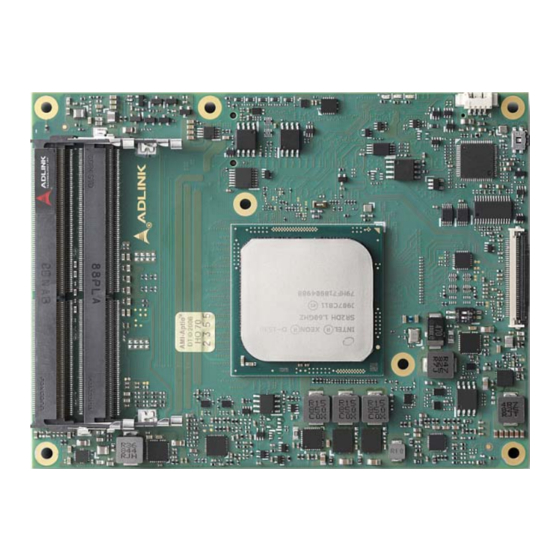
Summary of Contents for ADLINK Technology Express-BD74
- Page 1 Express-BD74 User’s Manual COM Express Basic Size Type 7 Module with up to 16-core Intel® Xeon® D Processor and Four SODIMM sockets Manual Rev.: Revision Date: May 25, 2020 Part Number: 50-1J098-1010 Leading EDGE COMPUTING...
- Page 2 Preface Copyright Copyright © 2019, 2020 ADLINK Technology, Inc. This document contains proprietary information protected by copyright. All rights are reserved. No part of this manual may be reproduced by any mechanical, electronic, or other means in any form without prior written permission of the manufacturer.
-
Page 3: Table Of Contents
Express-BD74 Table of Contents Preface ..........................ii List of Figures ........................v List of Tables........................vi Introduction........................1 Specifications ......................3 2.1. Core System .......................3 2.2. Expansion Busses ......................3 2.3. 10Gigabit Ethernet......................4 2.4. Gigabit Ethernet......................4 2.5. Network Controller Sideband Interface (NC-SI)............4 2.6. Multi I/O and Storage....................4 2.7. -
Page 4: Preface
4.7. PCIe x16-to-two-x8 Adapter Card................32 4.8. PCIe x8-to-two-x4 Adapter Card................32 Smart Embedded Management Agent (SEMA) .............33 5.1. Board Specific SEMA Functions................34 System Resources ....................37 6.1. System Memory Map....................37 6.2. Direct Memory Access Channels................39 6.3. Fixed I/O Address Range Map .................39 6.4. -
Page 5: List Of Figures
List of Figures Figure 1: Express-BD74 Functional Block Diagram.................7 Figure 2: Express-BD74 Mechanical Drawing..................8 Figure 3: Express-BD74 Connector, Switch and LED Locations ............25 Figure 4: Express-BD74 and the DB40 Debug Module ................ 26 Figure 5: Express-BD74 Switch Locations .................... 31 Figure 6: COM Express Mounting Methods .................. - Page 6 List of Tables Table 1: Express-BD74 AB/CD Pin Definitions ..................9 Table 2: 40-pin Debug Connector Pin Definition ................... 27 Table 3: Express-BD74 LED Descriptions .................... 28 Table 5: Fan Connector Pin Definition ....................29 Table 6: BIOS Select and Mode Configuration Switch Settings............31 Table 7: SEMA Onboard Voltage Monitor .....................
-
Page 7: Introduction
Express-BD74 1. Introduction The Express-BD74 is a COM Express® COM.0 R3.0 Basic Size Type 7 module supporting the 64-bit Intel® Xeon® processor D (formerly “Broadwell-DE”) system-on-chip (SoC) with up to 4 SO-DIMMs to boost system performance. The Express-BD74 is specifically designed for customers who need excellent computing performance with balanced power consumption and multiple 10G Ethernet connectivity in a long product life solution. - Page 8 This page intentionally left blank. Introduction...
-
Page 9: Specifications
Express-BD74 2. Specifications 2.1. Core System Intel® Xeon® processor D, Pentium® D processor (formerly “Broadwell-DE”) • Intel® Xeon® D1539 1.6/1.9 GHz 35W (8C, up to 2133MHz) (eTEMP) • Intel® Xeon® D1559 1.5/1.8 GHz 45W (12C, up to 2133MHz) (eTEMP) •... -
Page 10: 10Gigabit Ethernet
2.3. 10Gigabit Ethernet Intel® 10G Ethernet Controller Integrated on Processor • 10GbE Feature Support Two 10GBASE-KR (on CD connector) • Sideband signals (on CD connector) for 10GbE • 10G_INT • 10G_PHY_MDIO_SDA and 10G_PHY_MDC_SCL (manage/control signals between MAC and PHY) • 10G_PHY_CAP (PHY mode capability pin, used to indicate whether the PHY on carrier board needs I2C or MDIO signals from module) •... -
Page 11: Serial I/O On Module
Express-BD74 2.7. Serial I/O on Module Chipset: Nuvoton NCT5104D Note: two UART ports native from SoC instead of NCT5104D supported by build option Ports: 2x UARTs Rx/Tx only Console Redirection: COM 1 or COM 2 selectable in BIOS COM Port Description... -
Page 12: Power Specifications
2.11. Power Specifications AT and ATX mode (AT mode startup controlled by SEMA Board Controller) Power Modes ATX @ 12V±5%,/ 5Vsb ±5% or AT @ 12V ±5% Standard Voltage Input ATX @ 8.5-20V, 5Vsb ±5% or AT @ 8.5-20V Wide Voltage Input ACPI 5.0 compliant, Smart Battery support Power Management Supports C0, C1, C1E, C3, C6, S0, S4, S5, S5 ECO mode... -
Page 13: Functional Diagram
(port 0/1/2/3) UART0/1 LPC to UART NCT5014D TPM 2.0 Debug header LPC bus SMBus SMBus SPI 0 BIOS GPIO 4x GPO, 4x GPI PCA9535 SPI 1 BIOS GP I2C SEMA LM73 SPI_CS# Sensor Figure 1: Express-BD74 Functional Block Diagram Specifications... -
Page 14: Mechanical Drawing
View All dimensions are shown in millimeters. Tolerances should be ± 0.25mm, unless otherwise noted. The tolerances on the module connector locating peg holes (dimensions [16.50, 6.00] and [16.50, 18.00]) should be ± 0.10mm. Figure 2: Express-BD74 Mechanical Drawing Specifications... -
Page 15: Pinouts And Signal Descriptions
AB/CD Pin Definitions The Express-BD74 is a Type 7 module supporting up to 32 PCIe lanes and 10G Ethernet on the CD connector and NC-SI on the AB connector. In the table below, all standard pins of the COM Express specification are described, including those not supported on the Express-BD74. - Page 16 Row A Row B Row C Row D Name Name Name Name PCIE_TX13+ PCIE_RX13+ 10G_LED_SDA RSVD PCIE_TX13- PCIE_RX13- 10G_LED_SCL RSVD 10G_SFP_SDA1 10G_SFP_SCL1 PCIE_TX12+ PCIE_RX12+ 10G_SFP_SDA0 10G_SFP_SCL0 PCIE_TX12- PCIE_RX12- 10G_SDP0 10G_SDP1 GND (fixed) GND (fixed) GND (fixed) GND (fixed) USB2- USB3- 10G_KR_RX1+ 10G_KR_TX1+ USB2+...
- Page 17 VCC_12V A109 B109 C109 D109 GND (fixed) GND (fixed) GND (fixed) GND (fixed) A110 B110 C110 D110 Note: LPC and eSPI are muxed in the standard COM Express specification. The Express-BD74 only supports the LPC bus. Pinouts and Signal Descriptions...
-
Page 18: Signal Description Terminology
3.2. Signal Description Terminology The following terms are used in the COM Express AB/CD Signal Descriptions below. Input to the Module Output from the Module Bi-directional input/output signal Open drain output I 3.3V Input 3.3V tolerant I 5V Input 5V tolerant O 3.3V Output 3.3V signal level O 5V... -
Page 19: Ab Signal Descriptions
Express-BD74 3.3. AB Signal Descriptions 3.3.1. Network Controller Sideband Interface (NC-SI) Signal Description PU/PD Comment NCSI_CLK_IN Clock reference for receive, transmit I 3.3VSB PD 10k and control interface NCSI_RXD[1:0] Receive Data (from NC to BMC) O 3.3VSB PU 10k PU 10k that aligns with LAN chip 3.3VSB... - Page 20 3.3.3. SATA Signal Description PU/PD Comment SATA0_TX+ Serial ATA channel 0, Transmit O SATA AC coupled on Module SATA0_TX- Output differential pair. SATA0_RX+ Serial ATA channel 0, Receive Input I SATA AC coupled on Module SATA0_RX- differential pair. SATA1_TX+ Serial ATA channel 1, Transmit O SATA AC coupled on Module SATA1_TX-...
- Page 21 LPC serial interrupt I/O OD PU 8.2k 3.3V 3.3V LPC_CLK LPC clock output –33MHz nominal O 3.3V Note: eSPI and LPC buses are muxed. Express-BD74 module only supports LPC interface. 3.3.6. Signal Description PU/PD Comment USB0+ USB 1.1/ 2.0 compliant...
- Page 22 Signal Description PU/PD Comment USB1+ USB differential data pairs for Port 1 USB 1.1/ 2.0 compliant USB1- 3.3VSB USB2+ USB differential data pairs for Port 1 USB 1.1/ 2.0 compliant USB2- 3.3VSB USB3+ USB differential data pairs for Port 2 USB 1.1/ 2.0 compliant USB3- 3.3VSB...
- Page 23 Express-BD74 3.3.9. Miscellaneous Signal Description PU/PD Comment Output for audio enunciator, the “speaker” in O 3.3V PU 1k 3.3V Platform SPKR PC-AT systems specification Output indicating that a watchdog time-out O 3.3V PU 10k 3.3V event has occurred. THRM# Input from off-module temp sensor indicating an I 3.3VSB...
- Page 24 3.3.12. General Purpose I/O (GPIO) Signal Description PU/PD Comment GPO[0] General purpose output pins. O 3.3V PU 10K 3.3V After hardware RESET output low GPO[1] General purpose output pins. O 3.3V PU 10K 3.3V After hardware RESET output low GPO[2] General purpose output pins.
- Page 25 Express-BD74 Signal Description PU/PD Comment SUS_STAT# Indicates imminent suspend operation; used to notify LPC O 3.3VSB PU 10k devices. 3.3VSB Indicates system is in Suspend to RAM state. Active-low SUS_S3# O 3.3VSB output. An inverted copy of SUS_S3# on the carrier board (also known as “PS_ON”) may be used to enable the non-...
-
Page 26: Cd Signal Descriptions
3.4. CD Signal Descriptions 3.4.1. USB 3.0 Extension Signal Description PU/PD Comment USB_SSRX0- Additional Receive signal differential pairs for the I PCIE AC coupled off USB_SSRX0+ SuperSpeed USB data path on USB0 module USB_SSTX0- Additional Transmit signal differential pairs for O PCIE AC coupled on USB_SSTX0+... - Page 27 Express-BD74 3.4.3. 10G Ethernet 10GbE port 0/1 Signal Description PU/PD Comment 10G_KR_RX0+ 10GBASE-KR ports, Receive Input I KR AC coupled on differential paris Module 10G_KR_RX0- 10G_KR_RX1+ 10G_KR_RX1- 10G_KR_TX0+ 10GBASE-KR ports, Transmit Output O KR AC coupled on differential paris Carrier...
- Page 28 Signal Description PU/PD Comment 10G_SFP_SDA0 C Data signal, of the 2-wire I/O OD PU 2.2k management interface used by 10GbE 3.3VSB 3.3VSB 10G_SFP_SDA1 controller to access the management registers of an external Optical SFP+ module 10G_SFP_SCL0 C Clock signal, of the 2-wire I/O OD PU 2.2k management interface used by 10GbE...
- Page 29 Express-BD74 Signal Description PU/PD Comment PCIE_TX20+ PCI Express channel 20, Transmit Output O PCIE AC coupled on Module PCIE_TX20- differential pair. PCIE_RX20+ PCI Express channel 20, Receive Input I PCIE AC coupled off Module PCIE_RX20- differential pair. PCIE_TX21+ PCI Express channel 21, Transmit Output...
- Page 30 Signal Description PU/PD Comment PCIE_RX30+ PCI Express channel 30, Receive Input I PCIE AC coupled off Module PCIE_RX30- differential pair. PCIE_TX31+ D101 PCI Express channel 31, Transmit Output O PCIE AC coupled on Module PCIE_TX31- D102 differential pair. PCIE_RX31+ C101 PCI Express channel 31, Receive Input I PCIE AC coupled off Module...
-
Page 31: Connectors, Leds And Switches
Note: For SODIMM keep-out zone information, please refer to 2.17 Mechanical Drawing on page 8. 4.1. Connector, Switch and LED Locations BIOS Select and Mode Configuration Switch 40-pin Multi- Purpose BIOS Defaults Reset Switch 4-pin Figure 3: Express-BD74 Connector, Switch and LED Locations Connectors, LEDs and Switches... -
Page 32: Figure 4: Express-Bd74 And The Db40 Debug Module
Express-BD74 and the DB40 Debug Module For illustration purposes only Figure 4: Express-BD74 and the DB40 Debug Module Connectors, LEDs and Switches... -
Page 33: 40-Pin Debug Connector
Express-BD74 4.2. 40-pin Debug Connector FPC Connector Type: Molex 502790-4091 Pin Orientation 40-pin Debug Connector Pin Definition on the COM Express Module Pin Interface Signal Remark Interface Signal Remark VCC_SPI_IN TXD6 Program Program RXD6 interface interface (cont’d) SPI_BIOS_CS0# FUMD0 SPI_BIOS_CS1# PU 10k 3.3VSB... -
Page 34: Status Leds
Rebooted after WD RESET LED ON Rebooted after PWRBTN LED OFF Rebooted after RESET BTN LED OFF Note: only a RESET not initiated by the BMC can clear the WD LED (user action) Table 3: Express-BD74 LED Descriptions Connectors, LEDs and Switches... -
Page 35: Fan Connector
Express-BD74 4.4. Fan Connector Connector Type: JVE 24W1125A-04M00 Pin Orientation 1 2 3 4 Pin Assignment Name Signal FAN_PWMOUT FAN_TACHIN Ground Table 4: Fan Connector Pin Definition Connectors, LEDs and Switches... -
Page 36: Bios Setup Defaults Reset Button
4.5. BIOS Setup Defaults Reset Button To perform a hardware reset of BIOS default settings, perform the following steps: 1. Shut down the system. 2. Press the BIOS Setup Defaults RESET Button continuously and boot up the system. You can release the button when the BIOS prompt screen appears 3. -
Page 37: Switch Settings
Switch Locations BIOS Select and Mode Configuration Switch (SW3) Figure 5: Express-BD74 Switch Locations BIOS Select and Mode Configuration Switch The module has two BIOS chips and BIOS operation can be configured to "PICMG" and dual-BIOS "Failsafe" modes using the BIOS Select and Mode Configuration Switch (SW3), Pin 2. -
Page 38: Pcie X16-To-Two-X8 Adapter Card
4.7. PCIe x16-to-two-x8 Adapter Card The Express-BD74 can be used with the PCIe x16-to-two-x8 Adapter Card on the Express-BASE7 Reference Carrier to support bifurbication of the PCIe x16 interface. The card reroutes the PCIe x16 to two x8 and allows testing of two independent PCIe add-on cards with x8/x4/x2/x1 width. -
Page 39: Smart Embedded Management Agent (Sema)
Express-BD74 5. Smart Embedded Management Agent (SEMA) The onboard microcontroller (BMC) implements power sequencing and Smart Embedded Management Agent (SEMA) functionality. The microcontroller communicates via the System Management Bus with the CPU/chipset. The following functions are implemented: ‧ Total operating hours counter. Counts the number of hours the module has been run in minutes. -
Page 40: Board Specific Sema Functions
5.1.2. Main Current The BMC of the Express-BD74 implements a current monitor. The current can be read by calling the SEMA function “Get Main Current”. The function returns four 16-bit values divided in high-byte (MSB) and low-byte (LSB). These 4 values represent the last 4 currents drawn by the board. The values are sampled every 250ms. The order of the 4 values is NOT in chronological order. -
Page 41: Table 9: Sema Exception Codes
Express-BD74 5.1.4. Exception Codes In case of an error, the BMC drives a blinking code on the blue Status LED (LED1). The same error code is also reported by the BMC Flags register. The Exception Code is not stored in the Flash Storage and is cleared when the power is removed. -
Page 42: Table 10: Sema Bmc Flags
5.1.5. BMC Flags The BMC Flags register returns the last detected Exception Code since power-up and shows the BIOS in use and the power mode. Description [ 0 ~ 4 ] Exception Code 0 = AT mode [ 6 ] 1 = ATX mode 0 = Standard BIOS [ 7 ]... -
Page 43: System Resources
Express-BD74 6. System Resources 6.1. System Memory Map Memory Range Target Dependency/Comments 0000 0000h-000D FFFFh Main Memory TOM registers in Host controller 0010 0000h-TOM (Top of Memory) 000E 0000h-000E FFFFh LPC or SPI Bit6 in BIOS Decode Enable register is set... - Page 44 Memory Range Target Dependency/Comments FF40 0000h-FF4F FFFFh LPC or SPI(or PCI) Bit 0 in BIOS Decode Enable register is set FF00 0000h-FF0F FFFFh 128 KB anywhere in 4GB Integrated LAN Enable using BAR in D25:F0(Integrated LAN Controller range Controller MBARA) 4 KB anywhere in 4GB range Integrated LAN Enable using BAR in D25:F0(Integrated LAN Controller...
-
Page 45: Direct Memory Access Channels
Express-BD74 6.2. Direct Memory Access Channels Channel Number Data Width System Resource 8-bits Generic 8-bits Generic 8-bits Generic 8-bits Generic Reserved - cascade channel 16-bits Generic 16-bits Generic 16-bits Generic 6.3. Fixed I/O Address Range Map Hex Range Device 000-008... - Page 46 Hex Range Device 070-077 DMA Controller and LPC,PCI,or PCIE 081-083 084-086 089-08B 08C-08E 090-091 DMA Controller 093-09F DMA Controller Reset Generator 0A0-0A1 Interrupt Controller 0A4-0A5 0A8-0A9 0AC-0AD 0B0-0B1 Interrupt Controller 0B4-0B5 0B8-0B9 0BC-0BD 0B2-0B3 Power Management 0C0-0D1 DMA Controller 0D2-0DD 0DE-0DF FERR# / Interrupt Controller 170-177...
-
Page 47: Variable I/O Address Range Map
Express-BD74 6.4. Variable I/O Address Range Map Hex Range Device Anywhere in 64 KB I/O Space ACPI Anywhere in 64 KB I/O Space IDE Bus Master Anywhere in 64 KB I/O Space Native IDE Command Anywhere in 64 KB I/O Space... -
Page 48: Apic Interrupt Mapping
6.5. APIC Interrupt Mapping IRQ# Typical Intterupt Resource Using SERIRQ Cascade from 8259 #1 8254 Counter 0,HPET #0(Legacy mode) RTC,HPET #1(Legacy mode) Option for SCI,TCO Option for SCI,TCO HPET #2,Option for SCI,TCO HPET #3 FERR# logic SATA Primary SATA Secondary Internal devices are routable. -
Page 49: Pci Configuration Space Map
Express-BD74 6.6. PCI Configuration Space Map Bus Number Device Function Description Number Number Intel host Processor Bridge LPC Controller SATA Controller #1 SMBus Controller SATA Controller#2 USB EHCI Controller #1 PCI Express* Port 1 PCI Express Port 2 PCI Express Port 3... -
Page 50: Pci Interrupt Routing Map
6.7. PCI Interrupt Routing Map xHCI Gigabit Line Controller Ethernet Controller Int0 INTE:20 Int1 Int2 Int3 INTD:19 PCIE PCIE PCIE PCIE PCIE PCIE PCIE PCIE Line Port1 Port 2 Port 3 Port 4 Port 5 Port 6 Port 7 Port 8 Int0 INTA:16 INTB:17... -
Page 51: Bios Setup
Express-BD74 7. BIOS Setup 7.1. Menu Structure This section presents the six primary menus of the BIOS Setup Utility. Use the following table as a quick reference for the contents of the BIOS Setup Utility. The subsections in this section describe the submenus and setting options for each menu item. -
Page 52: Main
7.2. Main The Main Menu provides read-only information about your system and also allows you to set the System Date and Time. Refer to the tables below for details of the settings. 7.2.1. Main > BIOS Information Feature Options Description BIOS Vender Info only American Megatrends... - Page 53 Express-BD74 7.2.3. Main > Board Information Feature Options Description Board Information Submenu Board Information Info only Serial Number Info only Display SEMA serial Number. Manufacturing Date Info only Display SEMA manufacturing date. Last Repair Date Info only Display SEMA last repair date.
-
Page 54: Advanced
7.3. Advanced This menu contains the settings for most of the user interfaces in the system. 7.3.1. Advanced > Power Management Feature Options Description Power Management Info only Enable ACPI Auto Configuration Disabled Enable or Disables BIOS ACPI Auto Configuration. Enabled Enable Hibernation Disabled... - Page 55 Express-BD74 7.3.3. Advanced > System Management Feature Options Description System Management Info Only Version Info Only Display SEMA Module Version. SEMA Firmware Info Only Display SEMA Firmware Version. Build Date Info Only Display SEMA Firmware Build Date. SEMA Bootloader Info Only Display SEMA Bootloader Version.
- Page 56 7.3.4.1. Advanced > Thermal Management > Thermal and Fan Speed Feature Options Description Temperatures and Fan Speed Info Only CPU Temperature Info Only Current Info Only Display Current CPU Temperature Startup Info Only Display Startup CPU Temperature Info Only Display Min CPU Temperature Info Only Display Max CPU Temperature Board Temperature...
- Page 57 Express-BD74 7.3.6. Advanced > CSM Configuration Feature Options Description Compatibility Support Module Info only Configuration CSM Support Disableed Enabled / Disabled CSM Support. Enabled CSM16 Module Version Info only Display CSM16 Module Version GateA20 Active UPON REQUEST – GA20 can be disabled using Upon Request BIOS services.
- Page 58 7.3.7.1. Advanced > Super IO Configuration > Serial Port 1 Configuration (NCT5104D) Feature Options Description Serial Port 1 Configuration Submenu Set Parameters of Serial Port 1 (COMA). Serial Port 1 Configuration Info only Serial Port Disableed Enable or Disable Serial Port (COM). Enabled Device Settings Info Only...
- Page 59 Express-BD74 7.3.7.4. Advanced > Super IO Configuration > Serial Port 2 Configuration (W83627DHG) Feature Options Description Serial Port 2 Configuration Submenu Set Parameters of Serial Port 2 (COMB). Serial Port 2 Configuration Info only Serial Port Disableed Enable or Disable Serial Port (COM).
- Page 60 7.3.8. Advanced > Serial Console Redirection Feature Options Description COM1 Info only Console Redirection Console Redirection Enable or Disable. Enabled Disabled Console Redirection Settings Submenu The settings specify how the host computer and the remote computer (which the user is using) will exchange data.
- Page 61 Express-BD74 7.3.8.1. Advanced > Serial Console Redirection > Console Redirection Settings (If COM1 Enable) Feature Options Description COM1 Info only Console Redirection Settings Info only Teriminal Type VT100 Emulation: VT100+ ANSI: Extended ASCII char set. VT-UTF8 VT100: ASCII char set.
- Page 62 Feature Options Description Redirection After BIOS POST When Bootloader is selected, then Legacy Console Always Enable BootLoader Redirection is disabled before booting to legacy OS. When Always Enable is selected, then Legacy Console Redirection is enabled for legacy OS. Default setting for this option is set to Always Enable.
- Page 63 Express-BD74 Feature Options Description Putty KeyPad Select FunctionKey and KeyPad on Putty. VT100 Intel Linux XTERMR6 ESCN VT400 Redirection After BIOS POST When Bootloader is selected, then Legacy Console Always Enable BootLoader Redirection is disabled before booting to legacy OS.
- Page 64 Feature Options Description Resolution 100x31 Enabled On Legacy OS, the Number of Rows and Columns supported redirection Disabled Legacy OS Redirection On Legacy OS, the Number of Rows and Columns 80x24 Resolution 80x25 supported redirection Putty KeyPad Select FunctionKey and KeyPad on Putty. VT100 Intel Linux XTERMR6...
- Page 65 Express-BD74 Feature Options Description VT-UTF8 Combo Key Support Enable VT-UTF8 Combination Key Support for Enabled Disabled ANSI/VT100 terminals Recorder Mode With this mode enabled only text will be sent. Disabled Enabled This is to capture Terminal data. Resolution 100x31 Enabled...
- Page 66 7.3.9. Advanced > USB Configuration Feature Options Description USB Configuration Info Only USB Module Version Info Only Display USB Module Version USB Controllers: Info Only Display USB Controllers is XHCI or EHCI. USB Devices: Info Only Display attatcment USB deviecs. Legacy USB Support Enables Legacy USB support.
- Page 67 Express-BD74 7.3.11. Advanced > Miscellaneous Feature Options Description Miscellanous Info Only Control the PCI Express Root Port. Smart Battery Function Enable / Disable Battery Function Disable Enable I2C write protect control Active I2C write protect control Write protect Enabls or Disables 64bit capable Devices to be...
- Page 68 7.3.13. Advanced > Trusted Computing Feature Options Description TPM20 Device Found Info Only Security Device Support Disable Enables or Disable BIOS support for security device. Enable OS will not show Security Device. TCG EFI protocol and available. Active PCR banks Info Only Available PCR banks Info Only...
-
Page 69: Chipset
Express-BD74 7.4. Chipset 7.4.1. Chipset > Processor Configuration Feature Options Description Processor Configuration Info only Processor Socket Info only Display Processor Socket information Display Processor Socket information Processor ID Info only Display Processor Frequency information Processor Frequency Info only Display Processor Max Ratio information... - Page 70 7.4.2. Chipset > Advanced Power Management Configuration Feature Options Description Advanced Power Management Info only Configuration EIST (P-states) Disable When enabled, OS sets CPU frequency according load. When disabled, CPU frequency is set at max Enable non-turbo. Config TDP Option to disable/enable Config TDP Disable Enable CPU P State Control...
- Page 71 Express-BD74 7.4.2.2. Chipset > Advanced Power Management Configuration > CPU C State Control Feature Options Description CPU C State Control Info only C2C3TT Info only Display PCIE Port assigned to LAN Information. CPU C State Disable Enable the Enhanced Cx state of the CPU, takes effect after reboot.
- Page 72 7.4.4. Chipset > IIO Configuration Feature Options Description IIO Configuration Info only PCIe Hot Plug Enable/Disable PCIe Hot Plug globally Disable Enable Auto MANUAL PCIe ACPI Hot Plug Enable/Disable ACPI Hot Plug globally, or allow per- Disable port control. When Disabled,MSI is generated on HP Enable event.
- Page 73 Express-BD74 Chipset > IIO Configuration > IIO0 Configuration > Socket 0 PcieD02F0 – Port 2A Feature Options Description Socket 0 PcieD02F0 – Port Info only PCI-E Port In auto mode the BIOS will remove the EXP port if Auto there is no device or errors on that device and the Enable device is not HP capable.
- Page 74 Feature Options Description Gen3 Spec Mode PCIe Gen3 Spec Mode Auto 0.70 July 0.70 Sept 0.71 Sept Gen3 Phase2 Mode Hardware Adaptive Manual Gen3 DN Tx Present PCIe Gen3 Downstream Tx Present Auto P0 (-6.0/0.0 dB) P1 (-3.5/0.0 dB) P2 (-4.5/0.0 dB) P3 (-2.5/0.0 dB) P4 (0.0/0.0 dB) P5 (0.0/2.0 dB)
- Page 75 Express-BD74 Chipset > IIO Configuration > IIO0 Configuration > Socket 0 PcieD02F2 – Port 2C Feature Options Description Socket 0 PcieD02F2 – Port Info only PCI-E Port In auto mode the BIOS will remove the EXP port if Auto there is no device or errors on that device and the Enable device is not HP capable.
- Page 76 Feature Options Description Gen3 Spec Mode PCIe Gen3 Spec Mode Auto 0.70 July 0.70 Sept 0.71 Sept Gen3 Phase2 Mode Hardware Adaptive Manual Gen3 DN Tx Present PCIe Gen3 Downstream Tx Present Auto P0 (-6.0/0.0 dB) P1 (-3.5/0.0 dB) P2 (-4.5/0.0 dB) P3 (-2.5/0.0 dB) P4 (0.0/0.0 dB) P5 (0.0/2.0 dB)
- Page 77 Express-BD74 Chipset > IIO Configuration > IIO0 Configuration > Socket 0 PcieD03F0 – Port 3A Feature Options Description Socket 0 PcieD03F0 – Port Info only PCI-E Port In auto mode the BIOS will remove the EXP port if Auto there is no device or errors on that device and the Enable device is not HP capable.
- Page 78 Feature Options Description Gen3 Spec Mode PCIe Gen3 Spec Mode Auto 0.70 July 0.70 Sept 0.71 Sept Gen3 Phase2 Mode Hardware Adaptive Manual Gen3 DN Tx Present PCIe Gen3 Downstream Tx Present Auto P0 (-6.0/0.0 dB) P1 (-3.5/0.0 dB) P2 (-4.5/0.0 dB) P3 (-2.5/0.0 dB) P4 (0.0/0.0 dB) P5 (0.0/2.0 dB)
- Page 79 Express-BD74 7.4.4.2. Chipset > IIO Configuration > Intel VT for Directed I/O (VT-d) Feature Options Description Intel VT for Directeded I/O (VT-d) Info VTd Azalea VCp Optimizations Enable/Disable Azalea VCp Optimizations Disable Enable Intel VT for Directed Enable/Disable Intel Virtualization Technology for...
- Page 80 7.4.5.2. Chipset > PCH Configuration > PCI Express Configuration Feature Options Description PCIE Ports 1-4 Config To Configure PCI-E Port 1-4 of PCH. 4x1 Port 1x2 2x1 Port 2x2 Port 1x4 Port PCIE Ports 5-8 Config To Configure PCI-E Port 1-4 of PCH. 4x1 Port 1x2 2x1 Port 2x2 Port...
- Page 81 Express-BD74 Chipset > PCH Configuration > PCI Express Configuration > PCI Express Root Port1-8 Feature Options Description PCI Express Root Port Disabled Control the PCI Express Root Port. Enabled L1 Substates Disabled PCI Express L1 Substates settings. L1.1 L1.2 L1.1 & L1.2...
- Page 82 7.4.5.3. Chipset > PCH Configuration > PCH SATA Configuration Feature Options Description PCH SATA Configuration Info only Configure SATA as Identify the SATA port is connected to Solid State Drive or Hard Disk Drive AHCI SATA test mode Enabled Enable/Disable SATA test mode Disabled SATA Mode options Submenu...
- Page 83 Express-BD74 7.4.5.4. Chipset > PCH Configuration > USB Configuration Feature Options Description USB Precondition Precondition work on USB host controller and root Enabled ports for faster enumeration. Disabled xHCI Mode Smart Auto Mode of operation of xHCI controller. Auto Enabled...
-
Page 84: Security
7.5. Security 7.5.1. Security > Password Description Feature Options Description Password Description Info only Setup Administrator Password Enter Password Set Setup Administrator Password User Password Enter Password Set User Password Secure Boot Submenu Customizable Secure Boot settings. System Mode Info only Secure Boot Info only Vender Keys... -
Page 85: Boot
Express-BD74 7.6. Boot Feature Options Description Boot Configuration Info only Setup Prompt Timeout Number of seconds to wait for setup activation key. 65535(0xFFFF) means indefinite waiting. Bootup NumLock State Select the keyboard Number state. Ouiet Boot Disabled Select the keyboard NumLock state. -
Page 86: Save & Exit
7.7. Save & Exit Feature Options Description Save Changes and Exit Exit system setup after saving the changes. Discard Changes and Exit Exit system setup without saving any changes. Save Change and Reset Reset the system after saving the changes. Discard Changes and Reset Reset system setup without saving any changes. -
Page 87: Bios Checkpoints, Beep Codes
Express-BD74 8. BIOS Checkpoints, Beep Codes This section of this document lists checkpoints and beep codes generated by AMI Aptio BIOS. The checkpoints defined in this document are inherent to the AMIBIOS generic core, and do not include any chipset or board specific checkpoint definitions. -
Page 88: Status Code Ranges
8.1. Status Code Ranges Status Code Description Range 0x01 – 0x0B SEC execution 0x0C – 0x0F SEC errors 0x10 – 0x2F PEI execution up to and including memory detection 0x30 – 0x4F PEI execution after memory detection 0x50 – 0x5F PEI errors 0x60 –... - Page 89 Express-BD74 SEC Error Codes 0x0C – 0x0D Reserved for future AMI SEC error codes 0x0E Microcode not found 0x0F Microcode not loaded 8.2.2. SEC Beep Codes None 8.2.3. PEI Phase Status Code Description Progress Codes 0x10 PEI Core is started...
- Page 90 Status Code Description 0x35 CPU post-memory initialization. Boot Strap Processor (BSP) selection 0x36 CPU post-memory initialization. System Management Mode (SMM) initialization 0x37 Post-Memory North Bridge initialization is started 0x38 Post-Memory North Bridge initialization (North Bridge module specific) 0x39 Post-Memory North Bridge initialization (North Bridge module specific) 0x3A Post-Memory North Bridge initialization (North Bridge module specific) 0x3B...
- Page 91 Express-BD74 Status Code Description S3 Resume Error Codes 0xE8 S3 Resume Failed 0xE9 S3 Resume PPI not Found 0xEA S3 Resume Boot Script Error 0xEB S3 OS Wake Error 0xEC-0xEF Reserved for future AMI error codes Recovery Progress Codes 0xF0...
- Page 92 8.2.5. DXE Status Codes Status Code Description 0x60 DXE Core is started 0x61 NVRAM initialization 0x62 Installation of the South Bridge Runtime Services 0x63 CPU DXE initialization is started 0x64 CPU DXE initialization (CPU module specific) 0x65 CPU DXE initialization (CPU module specific) 0x66 CPU DXE initialization (CPU module specific) 0x67...
- Page 93 Express-BD74 Status Code Description 0x95 PCI Bus Request Resources 0x96 PCI Bus Assign Resources 0x97 Console Output devices connect 0x98 Console input devices connect 0x99 Super IO Initialization 0x9A USB initialization is started 0x9B USB Reset 0x9C USB Detect 0x9D USB Enable 0x9E –...
- Page 94 Status Code Description 0xB8 – 0xBF Reserved for future AMI codes 0xC0 – 0xCF OEM BDS initialization codes DXE Error Codes 0xD0 CPU initialization error 0xD1 North Bridge initialization error 0xD2 South Bridge initialization error 0xD3 Some of the Architectural Protocols are not available 0xD4 PCI resource allocation error.
-
Page 95: Oem-Reserved Checkpoint Ranges
Express-BD74 Status Code Description 0x10 System is waking up from the S1 sleep state 0x20 System is waking up from the S2 sleep state 0x30 System is waking up from the S3 sleep state 0x40 System is waking up from the S4 sleep state 0xAC System has transitioned into ACPI mode. - Page 96 This page intentionally left blank. BIOS Checkpoints, Beep Codes...
-
Page 97: Mechanical Information
Express-BD74 9. Mechanical Information 9.1. Board-to-Board Connectors To allow for different stacking heights, the receptacles for COM Express carrier boards are available in two heights: 5 mm and 8 mm. When 5 mm receptacles are chosen, the carrier board should be free of components. -
Page 98: Thermal Solution
9.2. Thermal Solution Note: For reference only. The actual COM Express module may differ from the illustrations below. 9.2.1. Heat Spreaders The function of the heat spreader is to ensure an identical mechanical profile for all COM Express modules. By using a heat spreader, the thermal solution that is built on top of the module is compatible with all COM Express modules. - Page 99 Express-BD74 Step 4: Use the four M2.5, L=8mm screws provided to fasten the heatsink to the module. Step 5: Place the COM Express module and heatsink assembly onto the connectors on the carrier board as shown. Then press down on the module until it is firmly seated on the carrier board.
- Page 100 Step 7: If you are installing a heatsink with a fan, plug the fan connector into the carrier board as shown. Mechanical Information...
-
Page 101: Mounting Methods
Express-BD74 9.3. Mounting Methods There are several standard ways to mount the COM Express module with a thermal solution onto a carrier board. There is the choice of Top and Bottom mounting. In Top mounting, the threaded standoffs are on the carrier board and the thermal solution is equipped with through-hole standoffs. -
Page 102: Standoff Types
9.4. Standoff Types The standoffs available for Top and Bottom mounting methods are shown below. Note that threaded standoffs are DIP type and through-hole standoffs are SMT type. Other types not listed are available upon request. 8mm through-hole standoff (SMT type) 8mm threaded standoff (DIP type) P/N: 33-72000-0080 P/N: 33-72015-0050... -
Page 103: Safety Instructions
Express-BD74 Safety Instructions Read and follow all instructions marked on the product and in the documentation before you operate your system. Retain all safety and operating instructions for future use. • Please read these safety instructions carefully. • Please keep this User‘s Manual for later reference. -
Page 104: Getting Service
5215 Hellyer Avenue, #110, San Jose, CA 95138, USA Tel: +1-408-360-0200 Toll Free: +1-800-966-5200 (USA only) Fax: +1-408-360-0222 Email: info@adlinktech.com ADLINK Technology (China) Co., Ltd. Address: 300 Fang Chun Rd., Zhangjiang Hi-Tech Park, Pudong New Area Shanghai, 201203 China Tel: +86-21-5132-8988 Fax: +86-21-5132-3588 Email: market@adlinktech.com...
Need help?
Do you have a question about the Express-BD74 and is the answer not in the manual?
Questions and answers