
Related Manuals for ADLINK Technology COM Express Express-ID7


Summary of Contents for ADLINK Technology COM Express Express-ID7
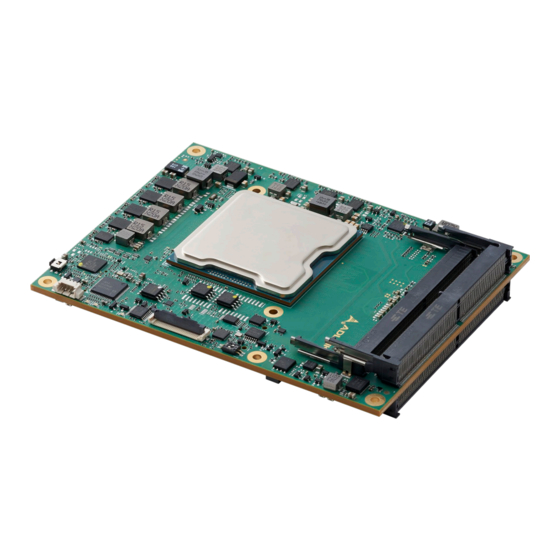
- Page 1 Express-ID7 User’s Guide PICMG COM.0 R3.1 Express-ID7 User’s Guide Revision: Rev. 1.0 Date: 2022-06-14 Part Number: 50M-00051-1000 Page 1 Copyright © 2022 ADLINK Technology, Inc.
- Page 2 Express-ID7 User’s Guide PICMG COM.0 R3.1 Revision History Revision Description Date Author Initial release 2022-06-14 Page 2 Copyright © 2022 ADLINK Technology, Inc.
-
Page 3: Preface
Product names mentioned herein are used for identification purposes only and may be trademarks / registered trademarks of respective companies. Copyright © 2022 ADLINK Technology Incorporated This document contains proprietary information protected by copyright. All rights are reserved. No part of this manual may be reproduced by any mechanical, electronic, or other means in any form without prior written permission of the manufacturer. - Page 4 Only install/attach and operate equipment on stable surfaces and/or recommended mountings; • If the equipment will not be used for long periods of time, turn off the power source and unplug the equipment. • Page 4 Copyright © 2022 ADLINK Technology, Inc.
- Page 5 Caution: This information indicates the possibility of minor physical injury, component damage, data loss, and/or program corruption. Warning: This information warns of possible serious physical injury, component damage, data loss, and/or program corruption. Page 5 Copyright © 2022 ADLINK Technology, Inc.
- Page 6 ADLINK Technology GmbH Hans-Thoma-Strasse 11, D-68163 Mannheim, Germany Tel: +49-621-43214-0 Fax: +49-621 43214-30 Email: emea@adlinktech.com Please visit the Contact page at www.adlinktech.com for information on how to contact the ADLINK regional office nearest you. Page 6 Copyright © 2022 ADLINK Technology, Inc.
-
Page 7: Table Of Contents
LPC Bus ..................................................................31 4.3.6 USB ....................................................................32 4.3.7 SPI Bus (BIOS only) ..............................................................33 4.3.8 Miscellaneous ................................................................34 4.3.9 SMBus .................................................................... 35 4.3.10 I2C Bus ................................................................... 35 4.3.11 General Purpose I/O (GPIO) ..........................................................36 Page 7 Copyright © 2022 ADLINK Technology, Inc. - Page 8 7.1.4 VxWorks ..................................................................56 8. Mechanical and Thermal ........................................................57 8.1. Module Dimensions ................................................................57 8.2. Thermal Solutions ................................................................. 58 8.2.1 Heatspreader: HTS ..............................................................58 8.2.2 Heatsink with Fan: THSF ............................................................59 Page 8 Copyright © 2022 ADLINK Technology, Inc.
-
Page 9: List Of Figures
Figure 4 – Express-ID7 and Debug Module ..................................................49 Figure 5 – Module mechanical dimensions ..................................................57 Figure 6 – Heatspreader HTS ........................................................58 Figure 9 – Heatsink with Fan: THSF ......................................................59 Page 9 Copyright © 2022 ADLINK Technology, Inc. -
Page 10: Introduction
SATA 6 Gb/s ports. Support for SMBus and I C is also provided. The module is equipped with SPI AMI EFI BIOS with CMOS backup, supporting embedded features such as remote console, hardware monitor, and watchdog timer. Page 10 Copyright © 2022 ADLINK Technology, Inc. -
Page 11: Specifications
Up to 128GB DDR4, three memory channel in total four SODIMM sockets, maximum 32GB per socket, ECC or non-ECC Up to 2933 MT/s memory speed (dependent on SKUs and 1DPC/2DPC usage) Four SODIMM sockets supported by build option and project basis Page 11 Copyright © 2022 ADLINK Technology, Inc. -
Page 12: Expansion Busses
Combined HSIO has a bandwidth up to the equivalent of 16 PCIe Gen3 lanes; PCIe lane 0-15, SATA, GbE and USB SSTX/RX are sourced from HSIO. Other: SMBus (system), I C (user), LPC bus Page 12 Copyright © 2022 ADLINK Technology, Inc. -
Page 13: Kr Ethernet
40GBASE-KR4 support requires the use of 4 KR lanes, which is supported by project basis (TBC). 2.4. GbE Ethernet Intel® Ethernet Controller I210 Series 1000/100/10 Mbit/s connections NC-SI and GBE0_SDP are supported on select SKU Page 13 Copyright © 2022 ADLINK Technology, Inc. -
Page 14: Multi I/O And Storage
Supported by Super I/O (W83627DHG) on carrier board 0x248 SER0, SER1 from SoC HSUART are supported by BOM option and project basis GPIO or SD 4 GPO and 4 GPI (GPI with interrupt, TBC) Page 14 Copyright © 2022 ADLINK Technology, Inc. -
Page 15: Trusted Platform Module (Tpm)
Power States: C0-C3, S0, S5, S5 ECO mode (WoL S5) ECO Mode support for deep S5 for 5Vsb power saving Note: For ATX power source, a minimum interval of 10ms is required from SUS_S3# fall to VCC_12V fall. Page 15 Copyright © 2022 ADLINK Technology, Inc. -
Page 16: Mechanical And Environmental
Shock and Vibration IEC 60068-2-64 and IEC-60068-2-27 MIL-STD-202F, Method 213B, Table 213-I, Condition A and Method 214A, Table 214-I, Condition D HALT tested Thermal Stress, Vibration Stress, Thermal Shock and Combined Test Page 16 Copyright © 2022 ADLINK Technology, Inc. -
Page 17: Block Diagram
Express-ID7 User’s Guide PICMG COM.0 R3.1 3. Block Diagram Figure 1 – Module functional block diagram Page 17 Copyright © 2022 ADLINK Technology, Inc. -
Page 18: Pinout And Signal Descriptions
COM.0 R3.1 specification. Signals described in the specification but not supported on the Express-ID7 are strikethrough STRIKETHROUGH A110 Figure 2 - Module rear side row and pin numbering Note: The 4 SO-DIMM (grey color) is supported by build option. Page 18 Copyright © 2022 ADLINK Technology, Inc. - Page 19 RSVD PCIE_CK_REF1- 10G_KR_RX2- 10G_KR_TX2- GND (fixed) GND (fixed) GND (fixed) GND (fixed) RSVD SPKR 10G_SFP_SDA3 10G_SFP_SCL3 RSVD I2C_CK 10G_SFP_SDA2 10G_SFP_SCL2 BIOS_DIS0# I2C_DAT 10G_PHY_RST_23 10G_PHY_CAP_23 THRMTRIP# THRM# 10G_PHY_RST_01 / CEI_RST# 10G_PHY_CAP_01 / CEI_PRSNT# Page 19 Copyright © 2022 ADLINK Technology, Inc.
- Page 20 RSVD RSVD PCIE_TX1+ PCIE_RX1+ RSVD RSVD PCIE_TX1- PCIE_RX1- PCIE_RX20+ PCIE_TX20+ WAKE0# PCIE_RX20- PCIE_TX20- GPI2 WAKE1# RAPID_SHUTDOWN PCIE_TX0+ PCIE_RX0+ PCIE_RX21+ PCIE_TX21+ PCIE_TX0- PCIE_RX0- PCIE_RX21- PCIE_TX21- GND (fixed) GND (fixed) GND (fixed) GND (fixed) Page 20 Copyright © 2022 ADLINK Technology, Inc.
- Page 21 D101 PCIE_TX31+ A102 SER1_RX B102 FAN_TACHIN C102 PCIE_RX31- D102 PCIE_TX31- A103 LID# B103 SLEEP# C103 D103 A104 VCC_12V B104 VCC_12V C104 VCC_12V D104 VCC_12V A105 VCC_12V B105 VCC_12V C105 VCC_12V D105 VCC_12V Page 21 Copyright © 2022 ADLINK Technology, Inc.
- Page 22 To stay at PCIE_CK_REF and only needing up to Gen3 at PCIe lane 16-31, a build option on module to re-route the clock for lane 16-31 is supported by project basis Note: 10G_LED_I2C (C36, C37) by build option supported by project basis. Note: USB_0_1_OC# (B44) and USB_2_3_OC# (A44) share the same source, from Ice Lake D. Page 22 Copyright © 2022 ADLINK Technology, Inc.
-
Page 23: Signal Terminology Descriptions
Pull-down strap. A Module output pin that is either tied to GND or is not connected. Used to signal Module capabilities to the Carrier Board. PU (pull-up) resistor on module PD (pull-down) resistor on module Page 23 Copyright © 2022 ADLINK Technology, Inc. -
Page 24: Ab Connector Signal Descriptions
Network Controller hardware arbitration input I 3.3VSB Left floating on module, that aligns with LAN chip NCSI_ARB_IN specification Network Controller hardware arbitration output NCSI_ARB_OUT 3.3VSB Note: NC-SI source from Intel® Ethernet Controller I210. Page 24 Copyright © 2022 ADLINK Technology, Inc. -
Page 25: Gigabit Ethernet
Gigabit Ethernet Controller 0 Software-Definable Pin. Can also be used for PU 10K Depends on the selection GBE0_SDP IO 3.3VSB IEEE1588 support such as 1pps signal. 3.3VSB of LAN controller Note: GBE0_ACT# and GBE0_LINK# share the same pin from LAN controller. Page 25 Copyright © 2022 ADLINK Technology, Inc. -
Page 26: Sata
ATA (parallel and serial) or SAS activity indicator, active low. O 3.3V PU 4.7K 3.3V 4.3.3.1. PCH HSIO Lane Assignments Name HSIO name on SOC Comment SATA0 HSIO 17 SATA1 HSIO 19 Page 26 Copyright © 2022 ADLINK Technology, Inc. -
Page 27: Pci Express
PCIE_RX8+ PCI Express channel 8, Receive Input differential pair. I PCIE AC coupled off Module PCIE_RX8- PCIE_TX9+ PCI Express channel 9, Transmit Output differential pair. O PCIE AC coupled on Module PCIE_TX9- Page 27 Copyright © 2022 ADLINK Technology, Inc. - Page 28 PCI Express Reference Clock output for all PCI Express and PCI O PCIE PCIE_CLK_REF- Express Graphics Lanes. PCIE_CLK_REF1+ O PCIE PCIE_CLK_REF1- Note: PCIE_CLK_REF1 (B29, B30) and GND (B28) are used for Gen4/3/2/1 speed at PCIe lane 16-31 Page 28 Copyright © 2022 ADLINK Technology, Inc.
- Page 29 Additional configurations supported by Intel® Xeon® D platform. Use caution when adopting these additional configurations. Note: Additional PCIe x1 at Lane 1 and Lane 5 are by build option supported by project basis. Page 29 Copyright © 2022 ADLINK Technology, Inc.
- Page 30 HSIO 5 PCIE6 HSIO 6 PCIE7 HSIO 7 PCIE8 HSIO 8 PCIE9 HSIO 9 PCIE10 HSIO 10 PCIE11 HSIO 11 PCIE12 HSIO 12 PCIE13 HSIO 13 PCIE14 HSIO 14 PCIE15 HSIO 15 Page 30 Copyright © 2022 ADLINK Technology, Inc.
-
Page 31: Lpc Bus
LPC_SERIRQ LPC serial interrupt I/O 3.3VSB PU 10K This Intel platform requires PU 3.3VSB LPC_CLK LPC clock output –33MHz nominal O 3.3VSB PD 10K The LPC_CLK frequency is 24MHz on this platform Page 31 Copyright © 2022 ADLINK Technology, Inc. -
Page 32: Usb
*Note: A pull-up for this line shall be present on the module. An open drain driver from a USB current monitor on the carrier board may drive this line low. 4.3.6.1. USB Root Segmentation All USB interfaces are derived from the xHCI controller. Page 32 Copyright © 2022 ADLINK Technology, Inc. -
Page 33: Spi Bus (Bios Only)
PU 10K Carrier shall pull to GND or leave not connected. 3.3VSB BIOS_DIS1# Selection strap to determine the BIOS boot device. PU 10K Carrier shall pull to GND or leave not connected 3.3VSB Page 33 Copyright © 2022 ADLINK Technology, Inc. -
Page 34: Miscellaneous
PD only when TPM on module. Active high. TPM chip has an internal pull down. This Modules implementing a TPM shall pull down signal is used to indicate Physical Presence to the TPM. Page 34 Copyright © 2022 ADLINK Technology, Inc. -
Page 35: Smbus
Source SEMA BMC as default (chipset by BOM 3.3VSB 3.3VSB option) I2C_DAT General purpose I²C port data I/O line I/O OD PU 2.2K Source SEMA BMC as default (chipset by BOM 3.3VSB 3.3VSB option) Page 35 Copyright © 2022 ADLINK Technology, Inc. -
Page 36: General Purpose I/O (Gpio)
Power rail tolerance 5V, 12V 3.3V 3.3V Note: SER0, SER1 source from EC is default setting. SER0, SER1 source from SoC’s HSUART is by build option by supported by project basis. HSUART has driver support limitation. Page 36 Copyright © 2022 ADLINK Technology, Inc. -
Page 37: Power And System Management
Trigger for Rapid Shutdown. Must be driven to 5V though a <=50-ohm source RAPID_ I CMOS Not supported impedance for ≥ 20 μs. SHUTDOWN 5VSB Page 37 Copyright © 2022 ADLINK Technology, Inc. -
Page 38: Power And Ground
Ground - DC power and signal and AC signal return A57, A60, A66, A70, A80, A90, path. A100, A110, B1, B11, B28, B21, B31, B41, B51, B60, B70, B80, B90, B100, B110 Page 38 Copyright © 2022 ADLINK Technology, Inc. -
Page 39: Cd Connector Signal Descriptions
Additional Transmit signal differential pairs for the SuperSpeed O PCIE AC coupled on module USB_SSTX3+ USB data path on USB3 4.4.1.1. USB Root Segmentation All USB interfaces are derived from the xHCI controller. Page 39 Copyright © 2022 ADLINK Technology, Inc. -
Page 40: Pci Express
PCIE_RX7+ PCI Express channel 7, Receive Input differential pair. I PCIE AC coupled off Module PCIE_RX7- 4.4.2.1. PCH HSIO Lane Assignments Refer to section 4.3.4.1 PCH HSIO Lane Assignments for detailed info. Page 40 Copyright © 2022 ADLINK Technology, Inc. -
Page 41: Kr Ethernet
Management Data I/O Interface mode data signal for serial data transfers between the MAC and an external PHY I2C mode I2C Data signal, of the 2-wire management interface used for serial data transfers between the MAC and the external PHY Page 41 Copyright © 2022 ADLINK Technology, Inc. - Page 42 I2C Clock signal, of the 2-wire management interface used by I/O OD PU 10K This pin is used for CEI mode CEI_SCL 10GbE controller to access the management registers of an 3.3VSB 3.3VSB external Optical SFP+ module Page 42 Copyright © 2022 ADLINK Technology, Inc.
- Page 43 Strapping signal for I2C or MDIO mode of Optical PHY 3.3VSB 3.3VSB Note: For detailed information about circuit design between the Ethernet controller, Optical Fiber/Copper PHY and firmware, please contact your local ADLINK representative. Page 43 Copyright © 2022 ADLINK Technology, Inc.
-
Page 44: Pci Express
PCIE_TX23+ PCI Express channel 23, Transmit Output differential pair. O PCIE AC coupled on Module PCIE_TX23- PCIE_RX23+ PCI Express channel 23, Receive Input differential pair. I PCIE AC coupled off Module PCIE_RX23- Page 44 Copyright © 2022 ADLINK Technology, Inc. - Page 45 If up to Gen3 speed is required on PCIe lane 16-31 and would like to use PCIe clock from A88/A89, a build option on the module can be supported by project basis. Page 45 Copyright © 2022 ADLINK Technology, Inc.
-
Page 46: Module Type Definition
Carrier Board logic may also implement a fault indicator such as an LED. TYPE10# In case of a type 10 module this pin signal is tied to GND through a 47K resistor No PD on the module. Page 46 Copyright © 2022 ADLINK Technology, Inc. -
Page 47: Power And Ground
C76, C80, C84, C87, C90, C93, C96, C100, C103, C110, D1, D2, D5, D8, D11, D14, D21, D31, D41, D51, D60, D67, D70, D73, D76, D80, D84, D87, D90, D93, D96, D100, D103, D110 Page 47 Copyright © 2022 ADLINK Technology, Inc. -
Page 48: Additional Features
This chapter describes connectors, LEDs, switches and additional items located on the module and not necessarily included in the PICMG standard spec- ification. The locations of these items are shown below: 30-pin Debug Status BIOS Boot Connector LEDs Select BIOS Default Reset Button Figure 3 – Module feature locations Page 48 Copyright © 2022 ADLINK Technology, Inc. -
Page 49: Debug Connector
Test points measurement of internal power rails I2C bus for BIOS POST code readout SPI BIOS programming interface Embedded Controller programming interface Figure 4 – Express-ID7 and Debug Module Page 49 Copyright © 2022 ADLINK Technology, Inc. -
Page 50: Status Leds
Rebooted after PWRBTN WD LED = LED OFF Rebooted after RESET BTN WD LED = LED OFF Note: Only a RESET not initiated by the BMC can clear the WD LED (user action) Page 50 Copyright © 2022 ADLINK Technology, Inc. -
Page 51: Exception Codes
PICMG COM.0 R3.1 5.3. Exception Codes Exception Code Error Message NOERROR NO_SUSCLK NO_SLP_S5 NO_SLP_S4 NO_SLP_S3 BIOS_FAIL RESET_FAIL RESETIN_FAIL NO_CB_PWROK CRITICAL_TEMP POWER_FAIL VOLTAGE_FAIL RSMRST_FAIL NO_VDDQ_PG NO_V1P05A_PG NO_VCORE_PG NO_SYS_GD NO_V5SBY NO_V3P3A NO_V5_DUAL NO_PWRSRC_GD NO_P_5V_3V3_S0_PG NO_SAME_CHANNEL NO_PCH_PG Page 51 Copyright © 2022 ADLINK Technology, Inc. -
Page 52: Fan Connector
Express-ID7 User’s Guide PICMG COM.0 R3.1 5.4. Fan Connector Connector type: JVE 24W1125A-04M00 4 3 2 1 Name Description FAN_PWMOUT FAN_TACHIN Page 52 Copyright © 2022 ADLINK Technology, Inc. -
Page 53: Bios Default Reset Button
2. Keep the BIOS Setup Defaults Reset Button pressed and boot up the system. You can release the button when the BIOS prompt screen appears 3. The BIOS prompt screen will display a confirmation that BIOS defaults have been reset and request that you reboot the system. Page 53 Copyright © 2022 ADLINK Technology, Inc. -
Page 54: Bios Boot Select
In either mode, BIOS Select and Mode Configuration Switch Pin 1 is used to select whether to boot from SPI0 or SPI1. Mode Pin 1 Pin 2 Boot from SPI0 (default) Boot from SPI1 Set BIOS to PICMG mode (default) Set BIOS to Failsafe BIOS mode Page 54 Copyright © 2022 ADLINK Technology, Inc. -
Page 55: Bios Checkpoints, Beep Codes
These PCI add-on cards show the value of I/O port 80h on an LED display. Aptio V Checkpoint and Beep Codes Download the Aptio V Checkpoint and Beep Codes from the AMI website at: www.ami.com/download/aptio-v-checkpoint-and-beep-codes Page 55 Copyright © 2022 ADLINK Technology, Inc. -
Page 56: Software Support
Windows Server 2019, Windows 10 IoT Enterprise LTSC Windows Server 2022 is scheduled to be supported in Q4. 7.1.2 Yocto Linux Yocto is scheduled to be supported in Q3 7.1.3 VxWorks VxWorks is scheduled to be supported in Q3 Page 56 Copyright © 2022 ADLINK Technology, Inc. -
Page 57: Mechanical And Thermal
All dimensions are shown in millimeters. Tolerances should be ± 0.25mm, unless otherwise noted. The tolerances on the module connector locating peg holes (dimensions [16.50, 6.00]&[16.50,18.00]) should be ± 0.10mm. Dimensions: mm Figure 5 – Module mechanical dimensions Page 57 Copyright © 2022 ADLINK Technology, Inc. -
Page 58: Thermal Solutions
Express-ID7 User’s Guide PICMG COM.0 R3.1 8.2. Thermal Solutions 8.2.1 Heatspreader: HTS Dimensions: mm M2.5*2pcs M2.5*5pcs 6.13 10.63 Figure 6 – Heatspreader HTS Page 58 Copyright © 2022 ADLINK Technology, Inc. -
Page 59: Heatsink With Fan: Thsf
Express-ID7 User’s Guide PICMG COM.0 R3.1 8.2.2 Heatsink with Fan: THSF M2.5*5pcs M2.5*2pcs 10.17 45.28 Dimensions: mm Figure 7 – Heatsink with Fan: THSF Page 59 Copyright © 2022 ADLINK Technology, Inc.
Need help?
Do you have a question about the COM Express Express-ID7 and is the answer not in the manual?
Questions and answers