
Subscribe to Our Youtube Channel
Related Manuals for ADLINK Technology Express-KL


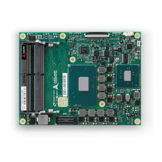
Summary of Contents for ADLINK Technology Express-KL
- Page 1 Express-KL User’s Manual COM Express Basic Size Type 6 Module with Mobile 7th Gen Intel® Core™ and Xeon® E3-1500 v6 Processors Manual Rev.: Revision Date: July 3, 2017 Part Number: 50-1J086-1000 Leading EDGE COMPUTING...
- Page 2 Preface Copyright Copyright 2017 ADLINK Technology, Inc. This document contains proprietary information protected by copyright. All rights are reserved. No part of this manual may be reproduced by any mechanical, electronic, or other means in any form without prior written permission of the manufacturer.
-
Page 3: Table Of Contents
Express-KL Table of Contents Preface ..........................ii List of Figures ........................v List of Tables........................vi Introduction........................1 Specifications ......................3 2.1. Core System ........................3 2.2. Expansion Busses......................3 2.3. Video ..........................4 2.4. Audio ..........................4 2.5. LAN ..........................4 2.6. Multi I/O and Storage ......................4 2.7. -
Page 4: Preface
6.2. Direct Memory Access Channels ..................41 6.3. I/O Map ......................... 41 6.4. Interrupt Request (IRQ) Lines ..................43 6.5. PCI Configuration Space Map..................44 6.6. PCI Interrupt Routing Map ....................45 6.7. SMBus Address Table ....................45 BIOS Setup.......................47 7.1. Menu Structure......................47 7.2. Main ..........................48 7.3. -
Page 5: List Of Figures
List of Figures Figure 1: Express-KL/KLE Functional Block Diagram................7 Figure 2: Express-KL/KLE Mechanical Drawing ..................8 Figure 3: Express-KL/KLE Connector, Switch and LED Locations ............29 Figure 4: Express-KL/KLE and the DB40 Debug Module ..............29 Figure 5: cExpress Switch Locations ....................34 Figure 6: COM Express Mounting Methods .................. - Page 6 List of Tables Table 1: Express-KL/KLE AB/CD Pin Definitions ..................9 Table 2: 40-pin Debug Connector Pin Definition ................... 30 Table 3: Express-KL/KLE LED Descriptions ..................31 Table 4: Fan Connector Pin Definition ....................32 Table 5: PCI Express Configuration Switch Settings ................34 Table 6: BIOS Select and Mode Configuration Switch Settings............
-
Page 7: Introduction
Express-KL 1. Introduction The Express-KL/KLE is a COM Express® COM.0 R2.1 Basic Size Type 6 module supporting the 64-bit 7 Generation Intel® Core™ and Xeon® processor E3 (codename “Kaby Lake-H”) with Mobile Intel® QM175, HM175, CM238 Chipset. The Express-KL/KLE is specifically designed for customers who need excellent graphics performance and high-level processing performance in a long product life solution. - Page 8 This page intentionally left blank. Introduction...
-
Page 9: Specifications
Mobile Intel® QM175, HM175 and CM238 Chipset (HM175 does not support Intel® AMT) Chipset AMI EFI with CMOS backup in 16MB SPI BIOS with Intel® AMT 11 support Embedded BIOS Express-KL (non-ECC memory support) CPU and Chipset Combinations • Core™ i7/i5 with QM175 Chipset •... -
Page 10: Video
2.3. Video Intel® Generation 9 Graphics core architecture Integrated on Processor • GPU Feature Support 3 independent and simultaneous combinations of DisplayPort/HDMI/LVDS graphics outputs (eDP optional in place of LVDS) • Encode/transcode HD content • Playback of high definition content including Blu-ray Disc •... -
Page 11: Serial I/O On Module
Express-KL 2.7. Serial I/O on Module Chipset: Nuvoton NCT5104D Ports: 2x UARTs Rx/Tx only Console Redirection: COM 1 or COM 2 selectable in BIOS COM Port Description IRQ Address Console redirection support COM 1 Supported by module (SER0, A98/A99), via NCT5104D... -
Page 12: Power Specifications
2.11. Power Specifications AT and ATX mode (AT mode startup controlled by SEMA Board Controller) Power Modes ATX: 12V±5% / 5Vsb ±5% or AT = 12V±5% Standard Voltage Input ATX: 8.5-20V, 5Vsb ±5% or AT @ 8.5-20V Wide Voltage Input ACPI 5.0 compliant, Smart Battery support Power Management Supports C1-C6, S0, S3, S4, S5 (Wake-on-USB S3/S4, WoL S3/S4/S5) -
Page 13: Functional Diagram
4x USB 3.0 (port 0/1/2/3) CM238 LPC to UART0/1 Chipset UART Debug header LPC bus SMBus GPIO SPI 0 BIOS SMBus 4x GPO, 4x GPI SPI 1 BIOS GP I2C SEMA DDC I2C LM73 SPI_CS# Sensor Figure 1: Express-KL/KLE Functional Block Diagram Specifications... -
Page 14: Mechanical Drawing
Side View All are dimensions shown in millimeters. Tolerances should be ± 0.25mm, unless otherwise noted. The tolerances of the module connector locating peg holes (dimensions [16.50, 6.00] and [16.50, 18.00]) should be ±0.10mm. Figure 2: Express-KL/KLE Mechanical Drawing Specifications... -
Page 15: Pinouts And Signal Descriptions
3.1. AB/CD Pin Definitions The Express-KL/KLE is a Type 6 module supporting USB 3.0 upgrade signals and DDI channels on the CD connector. All pins in the COM Express specification are described, including those not supported on the Express- KL/KLE. Those not supported on the Express-KL/KLE module are crossed out. - Page 16 Row A Row B Row C Row D Name Name Name Name USB6- USB7- DDI3_CTRLCLK_AUX+ DDI1_PAIR3+ USB6+ USB7+ DDI1_PAIR3- DDI3_CTRLDATA_AUX- USB_6_7_OC# USB_4_5_OC# DDI3_DDC_AUX_SEL RSVD USB4- USB5- DDI3_PAIR0+ DDI2_PAIR0+ USB4+ USB5+ DDI3_PAIR0- DDI2_PAIR0- GND (fixed) GND (fixed) GND (fixed) GND (fixed) USB2- USB3- DDI3_PAIR1+...
- Page 17 Express-KL Row A Row B Row C Row D Name Name Name Name GND (FIXED) GND (FIXED) GND (FIXED) GND (FIXED) LVDS_A_CK+ LVDS_B_CK+ PEG_RX9+ PEG_TX9+ LVDS_A_CK- LVDS_B_CK- PEG_RX9- PEG_TX9- LVDS_I2C_CK LVDS_BKLT_CTRL RSVD RSVD LVDS_I2C_DAT VCC_5V_SBY GPI3 VCC_5V_SBY PEG_RX10+ PEG_TX10+ RSVD...
-
Page 18: Signal Description Terminology
3.2. Signal Description Terminology The following terms are used in the COM Express AB/CD Signal Descriptions below. Input to the Module Output from the Module Bi-directional input/output signal Open drain output I 3.3V Input 3.3V tolerant I 5V Input 5V tolerant O 3.3V Output 3.3V signal level O 5V... -
Page 19: Ab Signal Descriptions
Express-KL 3.3. AB Signal Descriptions 3.3.1. Audio Signals Signal Pin # Description PU/PD Comment AC_RST# / Reset output to CODEC, active low. O 3.3VSB HDA_RST# AC_SYNC / Sample-synchronization signal to the O 3.3VSB HDA_SYNC CODEC(s). Serial data clock generated by the... - Page 20 3.3.3. LVDS Signal Pin # Description PU/PD Comment LVDS_A0+ / LVDS Channel A differential pairs O LVDS LVDS is default eDP_TX2+ support LVDS_A0- / eDP_TX2- LVDS_A1+ / eDP_TX1+ LVDS_A1- / eDP_TX1- LVDS_A2+ / eDP_TX0+ LVDS_A2- / eDP_TX0- LVDS_A3+ LVDS_A3- LVDS_A_CK+ / LVDS Channel A differential clock O LVDS eDP_TX3+...
- Page 21 Express-KL Signal Pin # Description PU/PD Comment eDP_BKLT_EN eDP backlight enable O 3.3V PD 10K eDP_BKLT_CTRL eDP backlight brightness control O 3.3V PD 100K eDP_AUX+ eDP AUX+ AC coupled off PCIE module eDP_AUX- eDP AUX- AC coupled off PCIE module...
- Page 22 Signal Pin # Description PU/PD Comment SATA2_TX+ Serial ATA channel 2, Transmit Output differential O SATA AC coupled on SATA2_TX- pair. Module SATA2_RX+ Serial ATA channel 2, Receive Input differential AC coupled on I SATA SATA2_RX- pair. Module SATA3_TX+ Serial ATA channel 3, Transmit Output differential O SATA AC coupled on SATA3_TX-...
- Page 23 Express-KL 3.3.8. Express Card Signal Pin # Description PU/PD Comment EXCD0_CPPE# PCI ExpressCard: PCI Express capable I 3.3V PU 10k EXCD1_CPPE# card request 3.3V EXCD0_PERST# PCI ExpressCard: reset O 3.3V EXCD1_PERST# 3.3.9. LPC Bus Signal Pin # Description PU/PD Comment...
- Page 24 Signal Pin # Description PU/PD Comment may drive this line low. . USB over-current sense, USB ports 4 and PU 10k Do not pull high on USB_4_5_OC# B38 I 3.3VSB 5. A pull-up for this line shall be present on 3.3VSB carrier the module.
- Page 25 Express-KL 3.3.13. Miscellaneous Signal Pin # Description PU/PD Comment SPKR Output for audio enunciator, the “speaker” in O 3.3V PC-AT systems Output indicating that a watchdog time-out O 3.3V PU 10k event has occurred. 3.3V THRM# Input from off-module temp sensor indicating an I 3.3VSB...
- Page 26 3.3.16. General Purpose I/O (GPIO) Signal Pin # Description PU/PD Comment GPO[0] General purpose output pins. O 3.3V PU 10K 3.3V After hardware RESET output low GPO[1] General purpose output pins. O 3.3V PU 10K 3.3V After hardware RESET output low GPO[2] General purpose output pins.
- Page 27 Express-KL Signal Pin # Description PU/PD Comment PWR_OK Power OK from main power supply. A high value indicates that PU 10k Should the power is good. This signal can be used to hold off Module 3.3VSB 3.3VSB have weak startup to allow carrier based FPGAs or other configurable pull up.
-
Page 28: Cd Signal Descriptions
3.4. CD Signal Descriptions 3.4.1. USB 3.0 Extension Signal Pin # Description PU/PD Comment USB_SSRX0- Additional Receive signal differential pairs for the I PCIE AC coupled off USB_SSRX0+ SuperSpeed USB data path on USB0 module USB_SSTX0- Additional Transmit signal differential pairs for O PCIE AC coupled on USB_SSTX0+... - Page 29 Express-KL 3.4.3. DDI Channels DDI 1 Signal Description PU/PD Comment DDI1_PAIR0+ Digital Display Interface1 O PCIE Pair 4 to Pair 6 differential pairs DDI1_PAIR0- Not supported DDI1_PAIR1+ DDI1_PAIR1- DDI1_PAIR2+ DDI1_PAIR2- DDI1_PAIR3+ DDI1_PAIR3- DDI1_PAIR4+ DDI1_PAIR4- DDI1_PAIR5+ DDI1_PAIR5- DDI1_PAIR6+ DDI1_PAIR6- DDI1_HPD Digital Display Interface Hot-Plug I 3.3V...
- Page 30 DDI 2 Signal Description PU/PD Comment DDI2_PAIR0+ Digital Display Interface2 differential O PCIE DDI2_PAIR0- pairs DDI2_PAIR1+ DDI2_PAIR1- DDI2_PAIR2+ DDI2_PAIR2- DDI2_PAIR3+ DDI2_PAIR3- DDI2_HPD I 3.3V PD 100K DDI2_CTRLCLK_AUX+ IF DDI2_DDC_AUX_SEL is floating I/O PCIE PD 100K DP2_AUX+ I/O OD IF DDI2_DDC_AUX_SEL pulled high HDMI2_CTRLCLK 3.3V PU 2.2K 3.3V when...
- Page 31 Express-KL DDI 3 Signal Description PU/PD Comment DDI3_PAIR0+ Digital Display Interface3 differential O PCIE DDI3_PAIR0- pairs DDI3_PAIR1+ DDI3_PAIR1- DDI3_PAIR2+ DDI3_PAIR2- DDI3_PAIR3+ DDI3_PAIR3- DDI3_HPD I 3.3V PD 100K DDI3_CTRLCLK_AUX+ IF DDI3_DDC_AUX_SEL is floating I/O PCIE PD 100K DP2_AUX+ I/O OD IF DDI3_DDC_AUX_SEL pulled high HDMI2_CTRLCLK 3.3V...
- Page 32 3.4.4. DDI to DP/HDMI Mapping Pin Name HDMI / DVI DDI1_PAIR0+ DP1_LANE0+ TMDS1_DATA2+ DDI1_PAIR0- DP1_LANE0- TMDS1_DATA2- DDI1_PAIR1+ DP1_LANE1+ TMDS1_DATA1+ DDI1_PAIR1- DP1_LANE1- TMDS1_DATA1- DDI1_PAIR2+ DP1_LANE2+ TMDS1_DATA0+ DDI1_PAIR2- DP1_LANE2- TMDS1_DATA0- DDI1_PAIR3+ DP1_LANE3+ TMDS1_CLK+ DDI1_PAIR3- DP1_LANE3- TMDS1_CLK- DDI1_PAIR4+ DDI1_PAIR4- DDI1_PAIR5+ DDI1_PAIR5- DDI1_PAIR6+ DDI1_PAIR6- DDI1_HPD DP1_HPD HDMI1_HPD...
- Page 33 Express-KL 3.4.5. PCI Express Graphics x16 (PEG) Signal Description PU/PD Comment PEG_RX0+ PCI Express Graphics transmit differential I PCIE AC couple off PEG_RX0- pairs. module PEG_RX1+ PEG_RX1- PEG_RX2+ PEG_RX2- PEG_RX3+ PEG_RX3- PEG_RX4+ PEG_RX4- PEG_RX5+ PEG_RX5- PEG_RX6+ PEG_RX6- PEG_RX7+ PEG_RX7- PEG_RX8+...
- Page 34 Signal Description PU/PD Comment PEG_TX15- D102 PCI Express Graphics lane reversal input PU 10K PEG_LANE_RV# D54 I 3.3V strap. 3.3V Pull low on the Carrier board to reverse lane order. 3.4.6. Module Type Definition Signal Pin # Description Comment TYPE0# The TYPE pins indicate to the Carrier Board the Pin-out Type that is Type 6 TYPE1#...
-
Page 35: Connector Pinouts On Module
Connector, Switch and LED Locations BIOS Defaults Reset Switch 4‐pin 40-pin Multi- Purpose Figure 3: Express-KL/KLE Connector, Switch and LED Locations Express-KL/KLE and the DB40 Debug Module For illustration purposes only Figure 4: Express-KL/KLE and the DB40 Debug Module Connector Pinouts on Module... -
Page 36: 40-Pin Debug Connector
4.2. 40-pin Debug Connector FPC Connector Type: FCI 59GF Flex 10042867 Pin Orientation 40-pin Debug Connector Pin Definition on the COM Express Module Interface Signal Remark Interface Signal Remark SPI Program VCC_SPI_IN SPI Power Input from flash tool TXD6 interface to module. -
Page 37: Status Leds
Rebooted after PWRBTN WD LED = LED OFF Rebooted after RESET BTN WD LED = LED OFF Note: only a RESET not initiated by the BMC can clear the WD LED (user action) Table 3: Express-KL/KLE LED Descriptions Connector Pinouts on Module... -
Page 38: Fan Connector
4.4. Fan Connector Connector Type: JVE 24W1125A-04M00 Pin Orientation 1 2 3 4 Pin Assignment Name Description FAN_PWMOUT FAN_TACHIN Ground Table 4: Fan Connector Pin Definition Connector Pinouts on Module... -
Page 39: Bios Setup Defaults Reset Button
Express-KL 4.5. BIOS Setup Defaults Reset Button To perform a hardware reset of BIOS default settings, perform the following steps: 1. Shut down the system. 2. Press the BIOS Setup Defaults RESET Button continuously and boot up the system. You can release the button when the BIOS prompt screen appears 3. -
Page 40: Switch Settings
4.6. Switch Settings Switch Locations BIOS Select and Mode Configuration Switch PCI Express Configuration Switch Figure 5: cExpress Switch Locations 4.6.1. PCI Express Configuration Switch. PCI Express Configuration Switch (also referred to as the PEG config. switch) allows you to configure the PCI Express x16 lanes from the CPU as 1 PCIe x16, 2 PCIe x8, or 1 PCIe x8 + 2 PCIe x4. -
Page 41: Table 6: Bios Select And Mode Configuration Switch Settings
Express-KL 4.6.2. BIOS Select and Mode Configuration Switch The module has two BIOS chips and BIOS operation can be configured to "PICMG" and dual-BIOS "Failsafe" modes using BIOS Select and Mode Configuration Switch (also referred to as the Failsafe BIOS switch), Pin 2. -
Page 42: Pcie X16-To-Two-X8 Adapter Card
4.7. PCIe x16-to-two-x8 Adapter Card The Express-KL/KLE can be used with the PCIe x16-to-two-x8 Adapter Card on the Express-BASE6 Reference Carrier to support bifurbication of the CPU's PEG interface (PCIe x16). The card reroutes the PCIe x16 to two x8 and allows testing of two independent PCIe add-on cards with x8/x4/x2/x1 width. -
Page 43: Smart Embedded Management Agent (Sema)
Express-KL 5. Smart Embedded Management Agent (SEMA) The onboard microcontroller (BMC) implements power sequencing and Smart Embedded Management Agent (SEMA) functionality. The microcontroller communicates via the System Management Bus with the CPU/chipset. The following functions are implemented: ‧ Total operating hours counter. Counts the number of hours the module has been run in minutes. -
Page 44: Board Specific Sema Functions
5.1.2. Main Current The BMC of the Express-KL/KLE implements a current monitor. The current can be read by calling the SEMA function “Get Main Current”. The function returns four 16-bit values divided in high-byte (MSB) and low-byte (LSB). These 4 values represent the last 4 currents drawn by the board. The values are sampled every 250ms. The order of the 4 values is NOT in chronological order. -
Page 45: Table 9: Sema Exception Codes
Express-KL 5.1.4. Exception Codes In case of an error, the BMC drives a blinking code on the blue Status LED (LED1). The same error code is also reported by the BMC Flags register. The Exception Code is not stored in the Flash Storage and is cleared when the power is removed. - Page 46 This page intentionally left blank. Smart Embedded Management Agent (SEMA)
-
Page 47: System Resources
Express-KL 6. System Resources 6.1. System Memory Map Address Range (decimal) Address Range (hex) Size Description (4GB-2MB) FFE00000 – FFFFFFFF 2 MB High BIOS Area (4GB-18MB) – (4GB-17MB-1) FEE00000 – FEEFFFFF 1 MB MSI Interrupts (4GB-20MB) – (4GB-19MB-1) FEC00000 – FECFFFFF... - Page 48 Hex Range Device 52h – 53h Timer/Counter LPC/eSPI NMI Controller Microcontroller NMI Controller1 Microcontroller NMI Controller1 Microcontroller NMI Controller1 RTC Controller RTC Controller RTC Controller RTC Controller RTC Controller RTC Controller 76h – 77h RTC Controller LPC/eSPI or PCIe 84h – 86h Reserved Reserved 8Ch –...
-
Page 49: Interrupt Request (Irq) Lines
Express-KL 6.4. Interrupt Request (IRQ) Lines PIC Mode IRQ# Typical Intterupt Resource Connected to Pin Available Counter 0 Keyboard controller IRQ1 via SERIRQ Cascade interrupt from slave PIC Serial Port 4 (COM4) IRQ3 via SERIRQ / PIRQ Note (1) Serial Port 3 (COM3) -
Page 50: Pci Configuration Space Map
IRQ# Typical Intterupt Resource Connected to Pin Available Secondary IDE controller IRQ15 via SERIRQ Note (1) P.E.G Root Port,Intel HDA, PCIE Port Note (1) 0/1/2/3/4/5/6, I.G.D., XHCI Controller PCIE Port 0/1/2/3/4/5/6, P.E.G Root Note (1) Port, PCIE Port 0/1/2/3/4/5/6, P.E.G Root Note (1) Port, SMBus Controller PCIE Port 0/1/2/3/4/5/6, P.E.G Root... -
Page 51: Pci Interrupt Routing Map
Express-KL 6.6. PCI Interrupt Routing Map P.E.G. Root xHCI ME Controller HD Audio Line Port Controller Controller Controller Int0 INTA:16 INTA:16 INTA:16 INTA:16 INTA:16 Int1 INTB:17 INTD:19 Int2 INTC:18 INTC:18 Int3 INTD:19 INTD:19 INTB:17 PCIE PCIE PCIE PCIE PCIE PCIE... - Page 52 This page intentionally left blank. System Resources...
-
Page 53: Bios Setup
Express-KL 7. BIOS Setup 7.1. Menu Structure This section presents the six primary menus of the BIOS Setup Utility. Use the following table as a quick reference for the contents of the BIOS Setup Utility. The subsections in this section describe the submenus and setting options for each menu item. -
Page 54: Main
7.2. Main The Main Menu provides read-only information about your system and also allows you to set the System Date and Time. Refer to the tables below the screen shot of this menu for details of the submenus and settings. 7.2.1. - Page 55 Express-KL 7.2.4. SPI Clock Frequency Feature Options Description Dual Output Fast Read support Info only Read Status Clock Frequency Info only Display frequency. Write Status Clock Frequency Info only Display frequency. Fast Read Status Clock Frequency Info only Display frequency.
- Page 56 7.2.5.3. System Management > Power Consumption Feature Options Description Power Consumption Info only Current Input Current Read only Display input current. Current Input Power Read only Display input power. VCC_CORE Read only Display actual voltage of the VCC_CORE. VCC_GT Read only Display actual voltage of the VCC_GT.
- Page 57 Express-KL Feature Options Description ATX/AT-Mode Read only Display ATX/AT-Mode. Exception Code Read only System exception reason. 7.2.5.6. System Management > Power Up Feature Options Description Power Up Info only Power Up watchdog Enabled The Power-Up Watchdog resets the system after a certain amount of time after power-up.
-
Page 58: Advanced
7.3. Advanced This menu contains the settings for most of the user interfaces in the system 7.3.1. Feature Options Description Info only Manufacturer, model, speed CPU Signature Info only Display CPU Signature. Microcode Revision Info only Display Microcode Revision. Processor Cores Info only Display Processor Cores. - Page 59 Express-KL Feature Options Description Power Limit 1 Time Window Power Limit 1 Time Window value in seconds. The value may vary from 0 to 28. 0 = default value (28 sec for Mobile and 8 sec for Desktop). Defines time window which TDP value should be maintained.
- Page 60 Feature Options Description Maximum Memory Frequency Maximun Memory Frequency Selections in MHz Auto 1067 1200 1333 1400 1600 1800 1867 2000 2133 2200 2400 2600 2667 2800 2933 3000 3200 3467 3733 4000 4133 Max TOLUD Maximum Value of TOLUD. Dynamic assignment Dynamic would adjust TOLUD automatically based on largest 1 GB...
- Page 61 Express-KL 7.3.3. Graphics Feature Options Description Graphics Configuration Info only IGFX VBIOS Version Info only Display VBIOS Version. Graphics turbo IMON current values supported (14- Graphics Turbo IMON Current Number entry field 31). Primary Display Select which of IGFX/PEG/PCI Graphics device...
- Page 62 Feature Options Description Hsync Polarity Hsync Polarity select Active High Active Low LVDS/eDP Backlight Mode Select LVDS Backlight control function. BMC Mode GTT Mode GTT LVDS/eDP Backlight Control Actual backlight value in percent of the maximum setting. 100% DDI port 1 No device DDI port 1 function choose to Display Port or HDMI.
- Page 63 Express-KL 7.3.4. SATA Feature Options Description SATA Controller(s) Enable/Disable SATA Device. Enabled Disabled SATA Mode Selection Determines how SATA controller(s) operate. AHCI Intel RST Premium SATA Speed Selection Default Indicates the maximum speed the SATA controller can support. Gen1 Gen2...
- Page 64 7.3.4.1. SATA > Software Feature Mask Configuration Feature Options Description Software Feature Mask Info only Configuration HDD Unlock If enabled, indicates that the HDD password unlock in Enabled the OS is enabled. Disabled LED Locate If enabled, indicates that the LED/SGPIO hardware is Enabled attached and ping to locate feature is enabled on the Disabled...
- Page 65 Express-KL 7.3.5.1. USB > USB Configuration Feature Options Description XHCI Disable Compliance Mode Options to disable Compliance Mode. Default is FALSE FALSE to not disable Compliance Mode. Set TRUE to TRUE disable Compliance Mode. XDCI Support Enable/Disable XDCI (USB OTG Device)
- Page 66 Feature Options Description OS Timer Set OS watchdog timer. BIOS Timer Set BIOS watchdog timer. 7.3.7. PCI and PCIe Feature Options Description PCI BUS Driver Version Info only PCI Devices Common Settings: Info only PCIE Ports 1-4 Configuration Configures PCI-E Port 1-4 of PCH. 4x1 Port [4X1]: Port 1-4 (x1) and Port 8 (x1) 1x2 2x1 Port...
- Page 67 Express-KL 7.3.7.1. PCI and PCIe > PEG Configuration Feature Options Description PEG Configuration Info only PCI Express Clock Gating Disabled Enable/Disable PCI Express Clock Gating for each root port. Enable DMI Link ASPM Control The control of Active State Power Management of the Disabled DMI Link.Auto is equal to POR setting.
- Page 68 Feature Options Description PCI Express Device Fatal Error Reporting Disabled Enable/Disable. Enable NFER PCI Express Device Non-Fatal Error Reporting Disabled Enable/Disable. Enable PCI Express Device Correctable Error Reporting Disabled Enable/Disable. Enable PCI Express Completion Timer TO Enable/Disable Disabled Enable SEFE Root PCI Express System Error on Fatal Error Disabled Enable/Disable.
- Page 69 Express-KL Feature Options Description PCIE LTR Lock PCIE LTR Configuration Lock. Disabled Enable PCH PCIe CLKREQ# Info Configuration PCIEX CLKREQ Mappin Default PCIE CLKREQ Override for default platform mapping. Override No CLKREQ Customer number 7.3.7.2. PCI and PCIe > PEG Configuration...
- Page 70 Feature Options Description Number of Presets to test 7, 3, 5 Choose between 7,3,5 and 0-9. Auto = current default for CPU 0 – 9 Auto Allow PERST# GPIO Usage Enable/Disable GPIO-based resets to PEG Enabled endpoint(s) during margin search, if needed Disable SW EQ Enable VOC Jitter Only Test Mode...
- Page 71 Express-KL Feature Options Description IO=3F8h; IRQ=3,4,5,6,7,10,11,12 IO=2F8h; IRQ=3,4,5,6,7,10,11,12 IO=3E8h; IRQ=3,4,5,6,7,10,11,12 IO=2E8h; IRQ=3,4,5,6,7,10,11,12 Device Mode Standard Serial Port Mode IrDA Active pulse 1.6 uS IrDA Active pulse 3/16 bit time ASKIR Mode NCT5104DSEC Super IO Info only Configuration Serial Port 1 Configuration Serial Port Enable/Disable Serial Port (COM).
- Page 72 Feature Options Description Emulation AT/ATX Emulation AT Select Emulation AT or ATX function. If this option set to [Emulation AT], BIOS will report no suspend functions to ACPI OS. In windows XP, it will make OS show shutdown message during system shutdown. 7.3.10.
- Page 73 Express-KL Feature Options Description 38400 57600 115200 Data Bits Select Data Bits. Parity Select Parity. None Even Mark Space Stop Bits Select number of stop bits. Flow Control Select flow control. None Hardware RTS/CTS VT-UTF8 Combo Key Support Disabled Enable VT-UTF8 Combination Key Support for ANSI/VT100 terminals.
- Page 74 Feature Options Description 70 C BMC Default This value is the temperature threshold of the Passive Passive Cooling Trip Point Disabled Cooling Trip Point. 80 C 90 C Critical Trip Point This value is the temperature threshold of the Critical Disabled Trip Point.
-
Page 75: Boot
Express-KL 7.4. Boot 7.4.1. Boot Configuration Feature Options Description Boot Configuration Info only Setup Prompt Timeout Enable/Disable the onboard SATA controllers. Bootup NumLock State Select SATA controller mode. Enable/Disable the PATA port. In fact this enables or Quiet Boot Disabled... -
Page 76: Security
Feature Options Description Video Do not launch Controls the execution of UEFI and Legacy Video OpROM. UEFI only Legacy only Other PCI devices UEFI OpROM For PCI devices other than Network, Mass storage or Video defines which OpROM to launch. Legacy OpROM 7.5. -
Page 77: Bios Checkpoints, Beep Codes
Express-KL 8. BIOS Checkpoints, Beep Codes This section of this document lists checkpoints and beep codes generated by AMI Aptio BIOS. The checkpoints defined in this document are inherent to the AMIBIOS generic core, and do not include any chipset or board specific checkpoint definitions. -
Page 78: Status Code Ranges
8.1. Status Code Ranges Status Code Description Range 0x01 – 0x0B SEC execution 0x0C – 0x0F SEC errors 0x10 – 0x2F PEI execution up to and including memory detection 0x30 – 0x4F PEI execution after memory detection 0x50 – 0x5F PEI errors 0x60 –... - Page 79 Express-KL SEC Error Codes 0x0C – 0x0D Reserved for future AMI SEC error codes 0x0E Microcode not found 0x0F Microcode not loaded 8.2.2. SEC Beep Codes None 8.2.3. PEI Phase Status Code Description Progress Codes 0x10 PEI Core is started...
- Page 80 Status Code Description 0x35 CPU post-memory initialization. Boot Strap Processor (BSP) selection 0x36 CPU post-memory initialization. System Management Mode (SMM) initialization 0x37 Post-Memory North Bridge initialization is started 0x38 Post-Memory North Bridge initialization (North Bridge module specific) 0x39 Post-Memory North Bridge initialization (North Bridge module specific) 0x3A Post-Memory North Bridge initialization (North Bridge module specific) 0x3B...
- Page 81 Express-KL Status Code Description S3 Resume Error Codes 0xE8 S3 Resume Failed 0xE9 S3 Resume PPI not Found 0xEA S3 Resume Boot Script Error 0xEB S3 OS Wake Error 0xEC-0xEF Reserved for future AMI error codes Recovery Progress Codes 0xF0...
- Page 82 8.2.5. DXE Status Codes Status Code Description 0x60 DXE Core is started 0x61 NVRAM initialization 0x62 Installation of the South Bridge Runtime Services 0x63 CPU DXE initialization is started 0x64 CPU DXE initialization (CPU module specific) 0x65 CPU DXE initialization (CPU module specific) 0x66 CPU DXE initialization (CPU module specific) 0x67...
- Page 83 Express-KL Status Code Description 0x95 PCI Bus Request Resources 0x96 PCI Bus Assign Resources 0x97 Console Output devices connect 0x98 Console input devices connect 0x99 Super IO Initialization 0x9A USB initialization is started 0x9B USB Reset 0x9C USB Detect 0x9D USB Enable 0x9E –...
- Page 84 Status Code Description 0xB8 – 0xBF Reserved for future AMI codes 0xC0 – 0xCF OEM BDS initialization codes DXE Error Codes 0xD0 CPU initialization error 0xD1 North Bridge initialization error 0xD2 South Bridge initialization error 0xD3 Some of the Architectural Protocols are not available 0xD4 PCI resource allocation error.
-
Page 85: Oem-Reserved Checkpoint Ranges
Express-KL Status Code Description 0x10 System is waking up from the S1 sleep state 0x20 System is waking up from the S2 sleep state 0x30 System is waking up from the S3 sleep state 0x40 System is waking up from the S4 sleep state 0xAC System has transitioned into ACPI mode. - Page 86 This page intentionally left blank. BIOS Checkpoints, Beep Codes...
-
Page 87: Mechanical Information
Express-KL 9. Mechanical Information 9.1. Board-to-Board Connectors To allow for different stacking heights, the receptacles for COM Express carrier boards are available in two heights: 5 mm and 8 mm. When 5 mm receptacles are chosen, the carrier board should be free of components. -
Page 88: Thermal Solution
9.2. Thermal Solution 9.2.1. Heat Spreaders The function of the heat spreader is to ensure an identical mechanical profile for all COM Express modules. By using a heat spreader, the thermal solution that is built on top of the module is compatible with all COM Express modules. - Page 89 Use the three M2.5, L=6mm screws provided to fasten the heatsink to the module. Note: The Express-KL/KLE uses two screws to attach the heatsink to the COM Express module. Step 4: Place the COM Express module and heatsink assembly onto the connectors on the carrier board as shown.
- Page 90 Step 6: If you are installing a heatsink with a fan, plug the fan connector into the carrier board as shown. Mechanical Information...
-
Page 91: Mounting Methods
Express-KL 9.3. Mounting Methods There are several standard ways to mount the COM Express module with a thermal solution onto a carrier board. In addition to the choice of 5 mm or 8mm board-to-board connectors, there is the choice of Top and Bottom mounting. -
Page 92: Standoff Types
9.4. Standoff Types The standoffs available for Top and Bottom mounting methods are shown below. Note that threaded standoffs are DIP type and through-hole standoffs are SMT type. Other types not listed are available upon request. 5mm through-hole standoff (SMT type) 5mm threaded standoff (DIP type) P/N: 33-72000-0050 P/N: 33-72016-0050... -
Page 93: Safety Instructions
Express-KL Safety Instructions Read and follow all instructions marked on the product and in the documentation before you operate your system. Retain all safety and operating instructions for future use. • Please read these safety instructions carefully. • Please keep this User‘s Manual for later reference. -
Page 94: Getting Service
5215 Hellyer Avenue, #110, San Jose, CA 95138, USA Tel: +1-408-360-0200 Toll Free: +1-800-966-5200 (USA only) Fax: +1-408-360-0222 Email: info@adlinktech.com ADLINK Technology (China) Co., Ltd. Address: 300 Fang Chun Rd., Zhangjiang Hi-Tech Park, Pudong New Area Shanghai, 201203 China Tel: +86-21-5132-8988 Fax: +86-21-5132-3588 Email: market@adlinktech.com...
Need help?
Do you have a question about the Express-KL and is the answer not in the manual?
Questions and answers