
Subscribe to Our Youtube Channel
Related Manuals for SMART Embedded Computing MVME3100


Summary of Contents for SMART Embedded Computing MVME3100
- Page 1 MVME3100 Single Board Computer Installation and Use P/N: 6806800M28H September 2019...
- Page 2 Computing” and the SMART Embedded Computing logo are trademarks of SMART Modular Technologies, Inc. All other names and logos referred to are trade names, trademarks, or registered trademarks of their respective owners. These materials are provided by SMART Embedded Computing as a service to its customers and may be used for informational purposes only. Disclaimer* SMART Embedded Computing (SMART EC) assumes no responsibility for errors or omissions in these materials.
-
Page 3: Table Of Contents
1.4.1 MVME3100 Layout........ - Page 4 4.10.1 MPC8540 PCI-X Interface ..........72 MVME3100 Single Board Computer Installation and Use (6806800M28H)
- Page 5 6.2.6 System Control Register ..........106 MVME3100 Single Board Computer Installation and Use (6806800M28H)
- Page 6 A.3 Thermally Significant Components ......... . 140 MVME3100 Single Board Computer Installation and Use (6806800M28H)
- Page 7 Related Documentation ............143 B.1 Smart Embedded Computing Documentation ....... . . 143 B.2 Manufacturers’...
- Page 8 Table of Contents MVME3100 Single Board Computer Installation and Use (6806800M28H)
- Page 9 MVME3100 Block Diagram ........
- Page 10 List of Figures MVME3100 Single Board Computer Installation and Use (6806800M28H)
- Page 11 MVME3100 Features Summary ........
- Page 12 Thermally Significant Components ........140 Table B-1 SMART Embedded Computing Publications ......143 Table B-2 Manufacturers’...
-
Page 13: About This Manual
Overview of Contents The MVME3100 Single Board Computer Installation and Use manual provides the information you will need to install and configure your MVME3100 single board computer and MVME721 rear transition module (RTM). It provides specific preparation and installation information, and data applicable to the board. - Page 14 Dual Universal Asynchronous Receiver/Transmitter Error Correction Code ENET Ethernet Environment Electrostatic Discharge File Allocation Table Fast Ethernet Controller FIFO First In First Out Floating Point Unit Geographic Address GENET Gigabit Ethernet Global Environment Variable MVME3100 Single Board Computer Installation and Use (6806800M28H)
- Page 15 Programmable Interrupt Controller PCI Mezzanine Card Input/Output Module Programmable Logic Device PCI Mezzanine Card (IEEE P1386.1) POST Power On S Test PrPMC Processor PMC QUART Quad Universal Asynchronous Receiver/Transmitter Real Time Clock MVME3100 Single Board Computer Installation and Use (6806800M28H)
- Page 16 Triple Speed Ethernet Controllers TSOP Thin Small Outline Package UART Universal Asynchronous Receiver/Transmitter UNIX UNIX operating system Input/Output Voltage VITA VMEbus International Trade Association VersaModule Eurocard VMEbus VersaModule Eurocard bus Vital Product Data Write Protect MVME3100 Single Board Computer Installation and Use (6806800M28H)
- Page 17 Logical OR Indicates a hazardous situation which, if not avoided, could result in death or serious injury Indicates a hazardous situation which, if not avoided, may result in minor or moderate injury MVME3100 Single Board Computer Installation and Use (6806800M28H)
- Page 18 6806800M28E May 2014 Re-branded to Artesyn template. Serial ATA Host Controller on page 72 Updated and Appendix B, Related Documentation on page 6806800M28D November 2013 Declaration of Conformity 6806800M28C December 2012 Added MVME3100 Single Board Computer Installation and Use (6806800M28H)
- Page 19 About this Manual Part Number Publication Date Description Safety Notes Sicherheitshinweise 6806800M28B August 2011 Updated 6806800M28A April 2011 EA version. MVME3100 Single Board Computer Installation and Use (6806800M28H)
- Page 20 About this Manual About this Manual MVME3100 Single Board Computer Installation and Use (6806800M28H)
-
Page 21: Safety Notes
The blade has been tested in a standard Smart Embedded Computing system and found to comply with the limits for a Class A digital device in this system, pursuant to part 15 of the FCC Rules, EN 55022 Class A respectively. - Page 22 Environment Environmental Damage Improperly disposing of used products may harm the environment.Always dispose of used products according to your country’s legislation and manufacturer’s instructions. MVME3100 Single Board Computer Installation and Use (6806800M28H)
-
Page 23: Sicherheitshinweise
Installieren Sie keine Ersatzteile oder führen Sie keine unerlaubten Veränderungen am Produkt durch, sonst verfällt die Garantie. Wenden Sie sich für Wartung oder Reparatur bitte an die für Sie zuständige Geschäftsstelle von Smart Embedded Computing. So stellen Sie sicher, dass alle sicherheitsrelevanten Aspekte beachtet werden. - Page 24 Kurzschlüssen führen. Betreiben Sie das Blade nur innerhalb der angegebenen Grenzwerte für die relative Luftfeuchtigkeit und Temperatur. Stellen Sie vor dem Einschalten des Stroms sicher, dass sich auf dem Blade kein Kondensat befindet. MVME3100 Single Board Computer Installation and Use (6806800M28H)
- Page 25 Sicherheitshinweise Umweltschutz Umweltverschmutzung Falsche Entsorgung der Produkte schadet der Umwelt. Entsorgen Sie alte Produkte gemäß der in Ihrem Land gültigen Gesetzgebung und den Empfehlungen des Herstellers. MVME3100 Single Board Computer Installation and Use (6806800M28H)
- Page 26 Sicherheitshinweise Sicherheitshinweise MVME3100 Single Board Computer Installation and Use (6806800M28H)
-
Page 27: Hardware Preparation And Installation
The RTM also provides two planar connectors for one PIM with rear I/O. Ordering and Support Information Refer to the data sheets for the MVME3100 SBC for a complete list of available variants and accessories. Refer to Appendix B, Related Documentation on page 143... -
Page 28: Unpacking Guidelines
This section discusses certain hardware and software tasks that may need to be performed prior to installing the board in a chassis. To produce the desired configuration and ensure proper operation of the MVME3100, you may need to carry out certain hardware modifications before installing the module. -
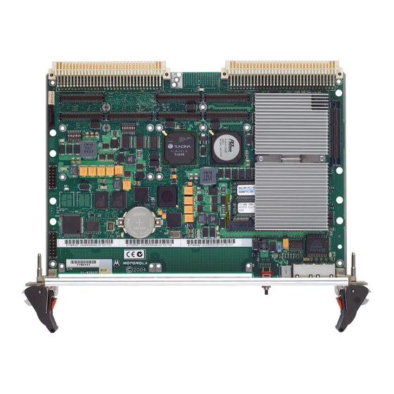
Page 29: Mvme3100 Layout
Table 1-4 for switch settings. There is one switch on the MVME721. Refer to Table Table 1-6 for switch settings. The MVME3100 is factory tested and shipped with the configuration described in the following sections. Figure 1-1 Board Layout U1014 U1050... -
Page 30: Configuration Switch (S4)
Normal MPC8540 TRST remain in the OFF the board to reset TRST SELECT mode where the board position unless a without resetting HRESET will assert TRST. MPC8540 emulator is the MPC8540 attached. JTAG/COP interface. MVME3100 Single Board Computer Installation and Use (6806800M28H) -
Page 31: Geographical Address Switch (S3)
Geographical Address Switch (S3) The TSi148 VMEbus Status register provides the VMEbus geographical address of the MVME3100. This switch reflects the inverted states of the geographical address signals. Applications not using the 5-row backplane can use the geographical address switch to assign a geographical address. -
Page 32: Pmc I/O Voltage Configuration
PMC sites will not function. Note that setting the PMC I/O voltage to 5.0V forces the PMC sites to operate in PCI mode instead of PCI-X mode. The default factory configuration is for 3.3V PMC I/O voltage. MVME3100 Single Board Computer Installation and Use (6806800M28H) -
Page 33: Rtm Seeprom Address Switch (S1)
Damage of the Product and Additional Devices and Modules Incorrect installation or removal of additional devices or modules may damage the product or the additional devices or modules. Before installing or removing additional devices or modules, read the respective documentation. MVME3100 Single Board Computer Installation and Use (6806800M28H) -
Page 34: Connecting To Peripherals
5. Slide the MVME3100 into the chassis until resistance is felt. 6. Simultaneously move the injector/ejector levers in an inward direction. 7. Verify that the MVME3100 is properly seated and secure it to the chassis using the two screws located adjacent to the injector/ejector levers. -
Page 35: Table 1-7 Mvme3100 Connectors
10/100/1000Mb/s Ethernet connector J41A COM port connector P1, P2 VME backplane connectors Table 1-8 MVME721 Rear Transition Module Connectors Connector Function J1A, J1B, J1C, J1D COM port connectors 10/100/1000Mb/s Ethernet connector 10/100Mb/s Ethernet connector MVME3100 Single Board Computer Installation and Use (6806800M28H) -
Page 36: Completing The Installation
Verify that hardware is installed and the power/peripheral cables connected are appropriate for your system configuration. Replace the chassis or system cover, reconnect the system to the AC or DC power source, and turn the equipment power on. MVME3100 Single Board Computer Installation and Use (6806800M28H) -
Page 37: Startup And Operation
On powering up, the MVME3100 brings up the MOTLoad prompt, MVME3100> Switches and Indicators The MVME3100 board provides a single push button switch that provides both abort and reset (ABT/RST) functions. When the switch is pressed for less than five seconds, an abort interrupt is generated to the processor. -
Page 38: Figure 2-1 Front Panel Leds And Connectors
Activity proportional to bandwidth utilization. GENET 1 Green Activity No activity Figure 2-1 Front Panel LEDs and Connectors PMC 2 PMC 1 SATA 1 ABORT/RESET USER 1 COM 1 FAIL SPEED G ENET 1 MVME3100 Single Board Computer Installation and Use (6806800M28H) -
Page 39: Table 2-2 Mvme721 Led Status Indicators
This indicator is illuminated to indicate a power supply fail Supply Fail (silkscreen) condition. SATA 0 Green SATA 0 activity indicator Activity (silkscreen) SATA 1 Green SATA 1 activity indicator Activity (silkscreen) MVME3100 Single Board Computer Installation and Use (6806800M28H) - Page 40 Poor SNR - receive errors detected Link Quality (silkscreen) Fast Fair SNR - close to data error threshold Blink Good SNR on link Green Green GENET 2 [Same as Link Quality DS2} MVME3100 Single Board Computer Installation and Use (6806800M28H)
-
Page 41: Motload Firmware
Implementation and Memory Requirements The implementation of MOTLoad and its memory requirements are product specific. The MVME3100 Single Board Computer (SBC) is offered with a wide range of memory (for example, DRAM, external cache, flash). Typically, the smallest amount of on-board DRAM that an Smart Embedded Computing SBC has is 32MB. -
Page 42: Tests
Manual. Test results and test status are obtained through the testStatus, errorDisplay, and taskActive commands. Refer to the appropriate command description page in the MOTLoad Firmware Package User’s Manual for more information. MVME3100 Single Board Computer Installation and Use (6806800M28H) -
Page 43: Command List
Block Copy blkFmt Block Format blkRd Block Read blkShow Block Show Device Configuration Data blkVe Block Verify blkWr Block Write Block Move Byte/Halfword/Word Assign/Delete/Display User-Program Break-Points Block Search Byte/Halfword/Word Block Verify Byte/Halfword/Word MVME3100 Single Board Computer Installation and Use (6806800M28H) - Page 44 Display (Show) File Discriptor flashLock Flash Memory Sector Lock flashProgram Flash Memory Program flashShow Display Flash Memory Device Configuration Data flashUnlock Flash Memory Sector Unlock Go Execute User-Program Direct (Ignore Break-Points) MVME3100 Single Board Computer Installation and Use (6806800M28H)
- Page 45 Display state of L3 Cache and L3CR register contents Memory Display Bytes/Halfwords/Words memShow Display Memory Allocation Memory Modify Bytes/Halfwords/Words mpuFork Execute program from idle processor mpuShow Display multi-processor control structure mpuStart Start the other MPU netBoot Network Boot (BOOT/TFTP) MVME3100 Single Board Computer Installation and Use (6806800M28H)
- Page 46 Symbol Table Attach Symbol Table Lookup stop Stop Date and Time (Power-Save Mode) taskActive Display the Contents of the Active Task Table Trace (Single-Step) User Program Trace (Single-Step) User Program to Address MVME3100 Single Board Computer Installation and Use (6806800M28H)
- Page 47 RAM Random Data Patterns testRtcAlarm RTC Alarm testRtcReset RTC Reset testRtcRollOver RTC Rollover testRtcTick RTC Tick testSerialExtLoop Serial External Loopback testSeriallntLoop Serial Internal Loopback testStatus Display the Contents of the Test Status Table MVME3100 Single Board Computer Installation and Use (6806800M28H)
-
Page 48: Using The Command Line Interface
MOTLoad then performs the specified action. An example of a MOTLoad command line prompt is shown below. The MOTLoad prompt changes according to what product it is used on (for example, MVME5500, MVME6100, MVME3100). MVME3100 Single Board Computer Installation and Use (6806800M28H) - Page 49 PAL Version 0.1 (Motorola MVME3100) If the partial command string cannot be resolved to a single unique command, MOTLoad will inform the user that the command was ambiguous. Example: MVME3100> te "te" ambiguous MVME3100> MVME3100 Single Board Computer Installation and Use (6806800M28H)
-
Page 50: Command Line Rules
For help with a specific test or utility the user can enter the following at the MOTLoad prompt: help <command_name> The help command also supports a limited form of pattern matching. Refer to the help command page. MVME3100 Single Board Computer Installation and Use (6806800M28H) -
Page 51: Firmware Settings
Firmware Settings The following sections provide additional information pertaining to the VME firmware settings of the MVME3100. A few VME settings are controlled by hardware jumpers while the majority of the VME settings are managed by the firmware command utility vmeCfg. - Page 52 Inbound Image 0 Ending Address Upper Register = 00000000 Inbound Image 0 Ending Address Lower Register = 1FFF0000 Inbound Image 0 Translation Offset Upper Register = 00000000 Inbound Image 0 Translation Offset Lower Register = 00000000 MVME3100> MVME3100 Single Board Computer Installation and Use (6806800M28H)
- Page 53 Outbound Image 2 Starting Address Upper Register = 00000000 Outbound Image 2 Starting Address Lower Register = B0000000 Outbound Image 2 Ending Address Upper Register = 00000000 Outbound Image 2 Ending Address Lower Register = B0FF0000 MVME3100 Single Board Computer Installation and Use (6806800M28H)
- Page 54 Outbound Image 7 Ending Address Lower Register = B1FF0000 Outbound Image 7 Translation Offset Upper Register = 00000000 Outbound Image 7 Translation Offset Lower Register = 4F000000 Outbound Image 7 2eSST Broadcast Select Register = 00000000 MVME3100> MVME3100 Single Board Computer Installation and Use (6806800M28H)
-
Page 55: Control Register/Control Status Register Settings
–e –i(0 - 7): Edits selected Inbound Window state vmeCfg –e –o(0 - 7): Edits selected Outbound Window state vmeCfg –e –r184: Edits PCI Miscellaneous Register state vmeCfg –e –r188: Edits Special PCI Target Image Register state MVME3100 Single Board Computer Installation and Use (6806800M28H) -
Page 56: Deleting Vme Settings
These transactions occur across the VMEbus in the case of the MVME3100. MOTLoad uses one of four mailboxes in the Tsi148 VME controller as the inter-board communication address (IBCA) between the host and the target. - Page 57 For further details on CR/CSR space, please refer to the VME64 Specification, listed in Appendix B, Related Documentation The MVME3100 uses a Discovery II for its VME bridge. The offsets of the mailboxes in the Discovery II are defined in the Discovery II User Manual, listed in...
-
Page 58: Alternate Boot Images And Safe Start
Some later versions of MOTLoad support Alternate Boot Images and a Safe Start recovery procedure. If Safe Start is available on the MVME3100, Alternate Boot Images are supported. With Alternate Boot Image support, the bootloader code in the boot block examines the upper 8MB of the flash bank for Alternate Boot images. - Page 59 'p [address]':execute specified (or default) POST image '?':this help screen 'h':this help screen boot> d Addr FFE00000 Size 00100000 Flags 00000003 Name: MOTLoad Addr FFD00000 Size 00100000 Flags 00000003 Name: MOTLoad boot> c MVME3100 Single Board Computer Installation and Use (6806800M28H)
-
Page 60: Boot Images
The image must be a multiple of 4 bytes in length (word-aligned). The content of the checksum location in the header is not part of the checksum calculation. The calculation assumes the location to be zero. The algorithm is implemented using the following code: MVME3100 Single Board Computer Installation and Use (6806800M28H) -
Page 61: Image Flags
USER or MCG boot images. POST images are expected, but not required, to return to the boot block code upon completion. DONT_AUTO_RUN MVME3100 Single Board Computer Installation and Use (6806800M28H) -
Page 62: User Images
RAM size in MB */ void flashPtr;/* ptr to this image in flash */ char boardType[16];/* name string, eg MVME3100 */ void globalData;/* 16K, zeroed, user defined */ unsigned int reserved[12]; } altBootData_t; MVME3100 Single Board Computer Installation and Use (6806800M28H) -
Page 63: 3.10.4 Alternate Boot Data Structure
Some later versions of MOTLoad support alternate boot images and a safe start recovery procedure. If safe start is available on the MVME3100, alternate boot images are supported. With alternate boot image support, the boot loader code in the boot block examines the upper 8MB of the flash bank for alternate boot images. - Page 64 Addr FFE00000 Size 00100000 Flags 00000003 Name: MOTLoad Addr FFD00000 Size 00100000 Flags 00000003 Name: MOTLoad boot> c NOPQRSTUVabcdefghijk#lmn3opqrsstuvxyzaWXZ Copyright Motorola Inc. 1999-2004, All Rights Reserved MOTLoad RTOS Version 2.0, PAL Version 0.b EA02 MVME3100> MVME3100 Single Board Computer Installation and Use (6806800M28H)
-
Page 65: Startup Sequence
MVME3100 Single Board Computer Installation and Use (6806800M28H) - Page 66 MOTLoad Firmware Startup Sequence MVME3100 Single Board Computer Installation and Use (6806800M28H)
-
Page 67: Functional Description
Chapter 4 Functional Description Introduction This chapter describes the MVME3100 and the MVME721 rear transition module (RTM) on a block diagram level. Features The following tables list the features of the MVME3100 and its RTM. Table 4-1 MVME3100 Features Summary... - Page 68 – One four-channel USB 2.0 controller: one channel for front panel – Two 10/100/1000 MPC8540 Ethernet channels for front-panel I/O and Ethernet rear P2 I/O – One 10/100 MPC8540 Ethernet channel for rear P2 I/O MVME3100 Single Board Computer Installation and Use (6806800M28H)
-
Page 69: Table 4-2 Mvme721 Rtm Features Summary
– Two RJ-45 connectors with integrated LEDs for rear panel I/O: one 10/100/1000 Ethernet channel and one 10/100 Ethernet channel – One PIM site with rear-panel I/O – Four status indicators: 10/100/1000 and 10/100 Ethernet link/speed and Miscellaneous activity LEDs MVME3100 Single Board Computer Installation and Use (6806800M28H) -
Page 70: Block Diagrams
Block Diagrams Figure 4-1 shows a block diagram of the overall board architecture and Figure 4-2 shows a block diagram of the MVME721 rear transition module architecture. Figure 4-1 MVME3100 Block Diagram MVME3100 Single Board Computer Installation and Use (6806800M28H) -
Page 71: Processor
Local Bus Interface The MVME3100 uses the MPC8540 local bus controller (LBC) for access to on-board flash and I/O registers. The LBC has programmable timing modes to support devices of different access times, as well as device widths of 8, 16, and 32 bits. -
Page 72: Flash Memory
Appendix B, Related Documentation, for more information. 4.6.2 Control and Timers Logic The MVME3100 control and timers logic resides on the local bus. This logic provides the following functions on the board: Local bus address latch Chip selects for flash banks and QUART ... -
Page 73: Ethernet Interfaces
Ethernet Interfaces The Maxim DS1375 RTC implemented on the MVME3100 provides an alarm interrupt routed to the MPC8540 programmable interrupt controller (PIC). A Maxim DS32KHz temperature controlled crystal oscillator provides the RTC reference. A battery backup circuit for the RTC is provided on board. -
Page 74: Pci/Pci-X Interfaces And Devices
4.10.2 TSi148 VME Controller The VMEbus interface for the MVME3100 is provided by the TSi148 ASIC. The TSi148 provides the required VME, VME extensions, and 2eSST functions. Transceivers are used to buffer the VME signals between the TSi148 and the VME backplane. Refer to the TSi148... -
Page 75: Pci-X-To-Pci-X Bridges
PCI-X-to-PCI-X Bridges The MVME3100 uses two of the four SATA channels. Channel 0 is routed to a SATA connector mounted on the front panel for an external drive connection. Channel 1 is routed to a planar SATA connector for an inside the chassis drive connection. Collocated with the planar connector is a SATA power connector. -
Page 76: Usb
USB power switch, which provides soft-start, current limiting, over-current detection, and power enable for port 1. Refer to the μPD720101 USB 2.0 Host Controller Data Sheet listed in Appendix B, Related Documentation, for additional details. MVME3100 Single Board Computer Installation and Use (6806800M28H) -
Page 77: Pmc Expansion
A board-level hard reset generates a reset for the entire board including the MPC8540, local PCI/PCI-X buses, Ethernet PHYs, serial ports, flash devices, and PLD(s). If the MVME3100 is configured as the VME system controller, the VME bus and local TSi148 reset input are also reset. -
Page 78: Debug Support
Debug Support 4.14 Debug Support The MVME3100 provides a boundary scan header for boundary scan test access and device programming. This board also provides a separate standard COP header for MPC8540 COP emulation. MVME3100 Single Board Computer Installation and Use (6806800M28H) -
Page 79: Pin Assignments
PMC Expansion Connector (J4) One 114-pin Mictor connector with a center row of power and ground pins is used to provide PCI expansion capability. The pin assignments for this connector are as follows: MVME3100 Single Board Computer Installation and Use (6806800M28H) -
Page 80: Table 5-1 Pmc Expansion Connector Pin Assignment
PMCINTB# PURST# PMCINTC# HRESET# PMCINTD# TRST# PEP# PCIXGNT# PCIXREQ# +12V -12V PERR# SERR# LOCK# No Connect DEVSEL# No Connect PCI XCAP TRDY# IRDY# STOP# FRAME# M66EN ACK64# No Connect REQ64# No Connect MVME3100 Single Board Computer Installation and Use (6806800M28H) - Page 81 PMC Expansion Connector Pin Assignment (continued) Signal Signal PCIRST# C/BE1# C/BE0# C/BE3# C/BE2# AD11 AD10 AD13 AD12 AD15 AD14 AD17 AD16 AD19 AD18 AD21 AD20 AD23 AD22 AD25 AD24 AD27 AD26 AD29 AD28 AD31 AD30 MVME3100 Single Board Computer Installation and Use (6806800M28H)
- Page 82 AD43 AD42 AD45 AD44 AD47 AD46 AD49 AD48 AD51 AD50 AD53 AD52 AD55 AD54 AD57 AD56 AD59 AD58 AD61 AD60 AD63 AD62 All PMC expansion signals are shared with the USB controller. MVME3100 Single Board Computer Installation and Use (6806800M28H)
-
Page 83: Ethernet Connectors (Genet1/J41B, Genet2/J2B, Enet1/J2A)
5.2.3 PCI Mezzanine Card (PMC) Connectors (J11 – J14, J21 – J23) There are seven 64-pin SMT connectors on the MVME3100 to provide 32/64-bit PCI interfaces and P2 I/O for one optional add-on PMC. PMC slot connector J14 contains the signals that go to VME P2 I/O rows A, C, D, and Z. - Page 84 PCI_RSVD +3.3Vaux PMCGNT1# PMCREQ1# +3.3V (VIO) AD31 AD28 AD27 AD25 C/BE3# AD22 AD21 AD19 +3.3V (VIO) AD17 FRAME# IRDY# DEVSEL# LOCK# PCI_RSVD PCI_RSVD +3.3V (VIO) AD15 AD12 AD11 AD09 C/BE0# AD06 AD05 MVME3100 Single Board Computer Installation and Use (6806800M28H)
-
Page 85: Table 5-4 Pmc Slot 1 Connector (J12) Pin Assignments
PMC Slot 1 Connector (J12) Pin Assignments Signal Signal +12V TRST# Not Used Not Used Not Used Pull-up +3.3V RST# Pull-down +3.3V Pull-down Not Used AD30 AD29 AD26 AD24 +3.3V IDSEL1 AD23 +3.3V AD20 AD18 AD16 C/BE2# MVME3100 Single Board Computer Installation and Use (6806800M28H) -
Page 86: Table 5-5 Pmc Slot 1 Connector (J13) Pin Assignments
GNT1B# Not Used Not Used EREADY0 Not Used ACK64# +3.3V No Connect (MONARCH#) Table 5-5 PMC Slot 1 Connector (J13) Pin Assignments Signal Signal Reserved C/BE7# C/BE6# C/BE5# C/BE4# +3.3V (VIO) PAR64 MVME3100 Single Board Computer Installation and Use (6806800M28H) - Page 87 AD60 AD59 AD58 AD57 +3.3V (VIO) AD56 AD55 AD54 AD53 AD52 AD51 AD50 AD49 AD48 AD47 AD46 AD45 +3.3V (VIO) AD44 AD43 AD42 AD41 AD40 AD39 AD38 AD37 AD36 AD35 AD34 AD33 MVME3100 Single Board Computer Installation and Use (6806800M28H)
-
Page 88: Table 5-6 Pmc Slot 1 Connector (J14) Pin Assignments
PMC1_19 (P2-C10) PMC1_20 (P2-A10) PMC1PMC1_21 (P2-C11) PMC1_22 (P2-A11) PMC1_23 (P2-C12) PMC1_24 (P2-A12) PMC1_25 (P2-C13) PMC1_26 (P2-A13) PMC1_27 (P2-C14) PMC1_28 (P2-A14) PMC1_29 (P2-C15) PMC1_30 (P2-A15) PMC1_31 (P2-C16) PMC1_32 (P2-A16) PMC1_33 (P2-C17) PMC1_34 (P2-A17) MVME3100 Single Board Computer Installation and Use (6806800M28H) -
Page 89: Table 5-7 Pmc Slot 2 Connector (J21) Pin Assignments
PMC1_58 (P2-A29) PMC1_59 (P2-C30) PMC1_60 (P2-A30) PMC1_61 (P2-C31) PMC1_62 (P2-A31) PMC1_63 (P2-C32) PMC1_64 (P2-A32) Table 5-7 PMC Slot 2 Connector (J21) Pin Assignments Signal Signal -12V INTC# INTD# INTA# PMCPRSNT1# INTB# PCI_RSVD +3.3Vaux MVME3100 Single Board Computer Installation and Use (6806800M28H) - Page 90 AD31 AD28 AD27 AD25 C/BE3# AD22 AD21 AD19 +3.3V (VIO) AD17 FRAME# IRDY# DEVSEL# LOCK# PCI_RSVD PCI_RSVD +3.3V (VIO) AD15 AD12 AD11 AD09 C/BE0# AD06 AD05 AD04 +3.3V (VIO) AD03 AD02 AD01 MVME3100 Single Board Computer Installation and Use (6806800M28H)
- Page 91 +12V TRST# Not Used Not Used Not Used Pull-up +3.3V RST# Pull-down +3.3V Pull-down Not Used AD30 AD29 AD26 AD24 +3.3V IDSEL1 AD23 +3.3V AD20 AD18 AD16 C/BE2# IDSEL1B TRDY# +3.3V STOP# MVME3100 Single Board Computer Installation and Use (6806800M28H)
-
Page 92: Table 5-8 Pmc Slot 2 Connector (J22) Pin Assignments
Not Used ACK64# +3.3V No Connect (MONARCH#) Table 5-9 PMC Slot 2 Connector (J23) Pin Assignments Signal Signal Reserved C/BE7# C/BE6# C/BE5# C/BE4# +3.3V (VIO) PAR64 AD63 AD62 AD61 AD60 AD59 AD58 MVME3100 Single Board Computer Installation and Use (6806800M28H) - Page 93 AD55 AD54 AD53 AD52 AD51 AD50 AD49 AD48 AD47 AD46 AD45 +3.3V (VIO) AD44 AD43 AD42 AD41 AD40 AD39 AD38 AD37 AD36 AD35 AD34 AD33 +3.3V (VIO) AD32 Reserved Reserved Reserved Reserved MVME3100 Single Board Computer Installation and Use (6806800M28H)
-
Page 94: Serial Port Connectors (Com1/J41A, Com2-Com5/J2A-D)
24-bit address and 16-bit data. The pin assignments for the P1 connector is as follows: Table 5-11 VMEbus P1 Connector Pin Assignments ROW Z ROW A ROW B ROW C ROW D Reserved BBSY* BCLR* Reserved ACFAIL* Reserved BG0IN* Reserved Reserved BG0OUT* Reserved BG1IN* Reserved MVME3100 Single Board Computer Installation and Use (6806800M28H) - Page 95 Reserved Reserved GA4_L Reserved Reserved Reserved IACK* Reserved Reserved IACKIN* SERA Reserved IACKOUT* SERB Reserved Reserved Reserved IRQ7* Reserved Reserved IRQ6* Reserved IRQ5* Reserved Reserved IRQ4* Reserved IRQ3* Reserved Reserved IRQ2* Reserved MVME3100 Single Board Computer Installation and Use (6806800M28H)
-
Page 96: Vmebus P2 Connector
The VME P2 connector is a 160-pin DIN. Row B of the P2 connector provides power to the MVME3100 and to the upper eight VMEbus address lines and additional 16 VMEbus data lines. The pin assignments for the P2 connector are the same for both the MVME3100 and MVME721, and are as follows:... - Page 97 PMC1_IO47 E2-3+ SP4RX PMC1_IO50 VD26 PMC1_IO49 PMC1_IO52 VD27 PMC1_IO51 E2-2- SP4TX PMC1_IO54 VD28 PMC1_IO53 E2-2+ PMC1_IO56 VD29 PMC1_IO55 SP4CTS PMC1_IO58 VD30 PMC1_IO57 E2-1- PMC1_IO60 VD31 PMC1_IO59 E2-1+ SP4RTS PMC1_IO62 PMC1_IO61 PMC1_IO64 PMC1_IO63 MVME3100 Single Board Computer Installation and Use (6806800M28H)
-
Page 98: Mvme721 Pmc I/O Module (Pim) Connectors (J10, J14)
PMC Host I/O connector J10 routes only power and ground from VME P2. There are no Host I/O signals on this connector. The MVME3100 routes PMC I/O from J14 of PMC Slot 1 to VME P2 rows A and C. The MVME721 routes these signals (pin-for-pin) from VME P2 to PMC I/O Module connector J14. -
Page 99: Planar Sata Power Connector (J30)
5.2.8 Planar SATA Power Connector (J30) There is one 2mm pitch header installed as a planar header on the MVME3100 board to provide power to a serial ATA (SATA) drive mounted on the board or somewhere within the chassis. The pin assignments for this header are as follows:... -
Page 100: Usb Connector (J27)
Pin Assignments USB Connector (J27) 5.2.9 USB Connector (J27) There is one USB Type A connector located on the MVME3100 front panel. The pin assignments are as follows: Table 5-15 USB Connector (J27) Pin Assignments Signal USB_VBUS (+5.0V) USB_DATA- USB_DATA+ 5.2.10... -
Page 101: Headers
Headers Headers This section describes the pin assignments of the Headers on the MVME3100. For Header settings, refer to Configuring Hardware on page 5.3.1 Boundary Scan Header (J24) The 14-pin boundary scan header provides an interface for programming the on-board PLDs and for boundary scan testing/debug purposes. - Page 102 No Connect CPU_SRST_L GND (optional pull-down) CPU_HRST_L KEY (no pin) CPU_CKSTPO_L 1. Pin 6 +3.3V has a resettable fuse and can supply up to 0.5A to power I/O buffers in the COP controller. MVME3100 Single Board Computer Installation and Use (6806800M28H)
-
Page 103: Memory Maps
FF7F FFFF MPC8540 CCS Registers FF80 0000 FFFF FFFF Flash Only FFFF F000 to FFFF FFFF is mapped after reset. The e500 core fetches the first instruction from FFFF FFFC following a reset. MVME3100 Single Board Computer Installation and Use (6806800M28H) -
Page 104: Motload's Processor Memory Map
Config cycles. 6.2.3 VME Memory Map The MVME3100 is fully capable of supporting both the PReP and the CHRP VME Memory Map examples with RAM size limited to 2GB. MVME3100 Single Board Computer Installation and Use (6806800M28H) -
Page 105: System I/O Memory Map
System resources including System Control and Status registers, external timers, and the QUART are mapped into a 16MB address range from the MVME3100 via the MPC8540 local bus controller (LBC). The memory map is defined in the following table, including the... - Page 106 External PLD Tick Timer 4 Compare Register E202 0048 External PLD Tick Timer 4 Counter Register E202 004C - E2FF Reserved FFFF 1. Byte read/write capable 2. 32-bit write only. 3. Reserved for future implementation. MVME3100 Single Board Computer Installation and Use (6806800M28H)
-
Page 107: System Status Register
System Status Register 6.2.5 System Status Register The MVME3100 board System Status register is a read-only register used to provide board status information. Table 6-4 System Status Register System Status Register – 0xE2000000 FIELD OPER RESET BD_TYPE Board type. These bits indicate the board type. -
Page 108: System Control Register
Memory Maps System Control Register 6.2.6 System Control Register The MVME3100 board System Control register provides board control bits. Table 6-5 System Control Register System Control Register - 0xE2000001 FIELD OPER RESET TSTAT_MASK Thermostat mask. This bit masks the DS1621 temperature sensor thermostat output. If this bit is cleared, the thermostat output is enabled to generate an interrupt. -
Page 109: System Indicator Register
6.2.7 System Indicator Register The MVME3100 board provides a System Indicator register that may be read by the system software to determine the state of the on-board status indicator LEDs or written to by system software to illuminate the corresponding on-board LEDs. -
Page 110: Flash Control/Status Register
Memory Maps Flash Control/Status Register 6.2.8 Flash Control/Status Register The MVME3100 provides software-controlled bank write protect and map select functions as well as boot block select, bank write protect, and activity status for the flash. Table 6-7 Flash Control/Status Register... -
Page 111: Pci Bus Status Registers
PCI-X bus A. A set condition indicates that bus A is operating in PCI-X mode. A cleared condition indicates PCI mode. PCI_A_64B PCI bus A 64-bit. A set condition indicates that bus A is enabled to operate in 64-bit mode. A cleared condition indicates 32-bit mode. RSVD MVME3100 Single Board Computer Installation and Use (6806800M28H) -
Page 112: Table 6-9 Pci Bus B Status Register
EREADY2. Indicates that the PrPMC module installed in PMC site 2 is ready for enumeration when set. If cleared, the PrPMC module is not ready for enumeration. If no PrPMC is installed, the bit is always set. 5.0V_VIO MVME3100 Single Board Computer Installation and Use (6806800M28H) -
Page 113: Table 6-10 Pci Bus C Status Register
PCI-X mode. A cleared condition indicates PCI mode. PCI_C_64B PCI bus C 64-bit. A set condition indicates that bus C is enabled to operate in 64-bit mode. A cleared condition indicates 32-bit mode. RSVD Reserved for future implementation. MVME3100 Single Board Computer Installation and Use (6806800M28H) -
Page 114: Interrupt Detect Register
Memory Maps Interrupt Detect Register 6.2.10 Interrupt Detect Register The MVME3100 provides an Interrupt Detect register that may be read by the system software to determine which of the Ethernet PHYs originated their combined (OR'd) interrupt. Table 6-11 Interrupt Detect Register... -
Page 115: Presence Detect Register
Presence Detect Register 6.2.11 Presence Detect Register The MVME3100 provides a Presence Detect register that may be read by the system software to determine the presence of optional devices. Table 6-12 Presence Detect Register Presence Detect Register - 0xE2000008 FIELD... -
Page 116: Pld Revision Register
PLD Revision Register 6.2.12 PLD Revision Register The MVME3100 provides a PLD Revision register that may be read by the system software to determine the current revision of the timers/registers PLD. Table 6-13 PLD Revision Register PLD Revision Register - 0xE2000009... -
Page 117: Test Register 1
TEST1 General-purpose 32-bit read/write field. 6.2.15 Test Register 2 The MVME3100 provides a second 32-bit test register that reads back the complement of the data in test register 1. Table 6-16 Test Register 2 Test Register 2 - 0xE2000014 31:0... -
Page 118: External Timer Registers
6.2.16 External Timer Registers The MVME3100 provides a set of tick timer registers for access to the four external timers implemented in the timers/registers PLD. These registers are 32-bit registers and are not byte writable. The following sections describe the external timer prescaler and control registers. - Page 119 Tick Timer 3 Control Register - 0xE2020030 (32 bits) Tick Timer 4 Control Register - 0xE2020040 (32 bits) OPER RESET Enable counter. When this bit is high, the counter increments. When this bit is low, the counter does not increment. MVME3100 Single Board Computer Installation and Use (6806800M28H)
-
Page 120: 6.2.16.3 Compare Registers
For periodic interrupts, this equation should be used to calculate the compare register value for a specific period (T): Compare register value = T (us) MVME3100 Single Board Computer Installation and Use (6806800M28H) -
Page 121: 6.2.16.4 Counter Registers
Geographical Address Register The VMEbus Status register in the TSi148 provides the VMEbus geographical address of the MVME3100. This register reflects the inverted states of the geographical address pins at the 5-row, 160-pin P1 connector. MVME3100 Single Board Computer Installation and Use (6806800M28H) - Page 122 Memory Maps Geographical Address Register MVME3100 Single Board Computer Installation and Use (6806800M28H)
-
Page 123: Programming Details
Chapter 7 Programming Details Introduction This chapter includes additional programming information for the MVME3100 single board computer. Items discussed include: MPC8540 Reset Configuration MPC8540 Interrupt Controller Local Bus Controller Chip Select Assignments Two-Wire Serial Interface User Configuration EEPROM VPD EEPROM... -
Page 124: Mpc8540 Reset Configuration
MPC8540 Reset Configuration MPC8540 Reset Configuration The MVME3100 supports the power-on reset (POR) pin sampling method for MPC8540 reset configuration. The states of the various configuration pins on the MPC8540 are sampled when reset is deasserted to determine the desired operating modes. The following table describes the configuration options and the corresponding default setting. - Page 125 TSEC2 controller uses GMII protocol (or RGMII if TSEC2 configured in reduced TSEC2_ TSEC2 Protocol mode) Resistor TXD7 Configuration TSEC2 controller uses TBI protocol (or RTBI if TSEC2 configured in reduced mode) MVME3100 Single Board Computer Installation and Use (6806800M28H)
- Page 126 RapidIO Device ID Fixed Unconnected Inputs TXD [2:4] (3 lower-order bits) CPU boot hold off mode CPU Boot e500 core boots LA27 Resistor Configuration without waiting for configuration by an external master MVME3100 Single Board Computer Installation and Use (6806800M28H)
- Page 127 1 added buffer delay 0 added buffer delays Agent of RapidIO and PCI/PCI-X MPC8540 Agent of a RapidIO LWE [2:3] _L Resistors Host/Agent Agent of a PCI/PCI-X Configuration Host of both RapidIO and PCI/PCI-X MVME3100 Single Board Computer Installation and Use (6806800M28H)
- Page 128 LGPL3, LGPL5 Fixed Boot sequencer Configuration enabled with extended I2C address mode Boot sequencer disabled General-purpose POR configuration vector to General-Purpose LAD [28:31] Resistor be placed in POR Configuration CPPORCR register bits MVME3100 Single Board Computer Installation and Use (6806800M28H)
- Page 129 Local bus LAD[0:31] is sampled during POR, but only LAD[28:31] are configurable by resistor option. Software can use this value to inform the firmware or operating system about initial board configuration. ECC signals from memory devices must be disconnected. MVME3100 Single Board Computer Installation and Use (6806800M28H)
-
Page 130: Mpc8540 Interrupt Controller
Programming Details MPC8540 Interrupt Controller MPC8540 Interrupt Controller The MVME3100 uses the MPC8540 integrated programmable interrupt controller (PIC) to manage locally generated interrupts. Currently defined external interrupting devices and interrupt assignments, along with corresponding edge/levels and polarities, are shown in the following table. -
Page 131: Local Bus Controller Chip Select Assignments
3. 32-bit timer registers are byte readable, but must be written as 32 bits. Two-Wire Serial Interface A two-wire serial interface for the MVME3100 is provided by an I C compatible serial controller integrated into the MPC8540. The MPC8540 I... -
Page 132: User Configuration Eeprom
1. Each SPD defines the physical attributes of each bank or group of banks. If both banks of a SODIMM are populated they are the same speed and memory size. 2. This is a dual address serial EEPROM. 3. The device address is user selectable using switches on the RTM. The recommended address setting for the MVME3100 is $AA. User Configuration EEPROM The MVME3100 board provides two 64KB dual address serial EEPROMs for a total of 128KB user configuration storage. -
Page 133: Rtm Vpd Eeprom
VPD flash packet information. The following table defines the supported flash density options for each bank. The factory configuration for the MVME3100-1152 is one bank of 64MB and for the MVME3100-1263 it is one bank of 128MB. -
Page 134: Table 7-6 Flash Options
S29GL512N 512 Mbit A hardware flash bank write protect switch is provided on the MVME3100 to enable write protection of both physical banks. Regardless of the state of the software flash write protect bit in the Flash Control/Status register, write protection is enabled for both banks when this switch is ON. -
Page 135: Pci Idsel Definition
Primary PMC1 0b0_0001 IRQ5 IRQ6 IRQ7 IRQ4 Secondary PMC2 0b0_0010 IRQ6 IRQ7 IRQ4 IRQ5 Primary PMC2 0b0_0011 IRQ7 IRQ4 IRQ5 IRQ6 Secondary uPD740101 0b0_0000 IRQ4 IRQ5 IRQ6 (PCI6520-2) 21150 on 0b0_0100 PMCSpan MVME3100 Single Board Computer Installation and Use (6806800M28H) -
Page 136: Pci Arbitration Assignments
PCI Arbitration Assignments The integrated PCI/X arbiters internal to the MPC8540 and the PCI6520 bridges provide PCI arbitration for the MVME3100. The MPC8540 provides arbitration support for itself and the four PCI-X devices on PCI bus A. MVME3100 Single Board Computer Installation and Use (6806800M28H) -
Page 137: Clock Distribution
PCI6520. One secondary arbiter provides arbitration for the PMC sites on PCI bus B, and the other provides arbitration for the PMCspan and USB host controller on PCI bus The arbitration assignments on the MVME3100 are shown in the follow table so that software may set arbiter priority assignments if necessary. -
Page 138: Table 7-10 Clock Assignments
3.3V Buffer Oscillator/ CLK25_33V_PLD 3.3V Buffer Control and Timers CCB_CLK/8 (333 CLK_LBC MPC8540 3.3V MHz/8) QUART CLK_UART 1.8432 Oscillator 3.3V sATA CLK25 Oscillator 3.3V CLK48 Oscillator 3.3V CLK32 32.768 kHz Crystal 3.3V MVME3100 Single Board Computer Installation and Use (6806800M28H) -
Page 139: Mpc8540 Real-Time Clock Input
(LCRR[CLKDIV]). For proper operation of the local bus, CLKDIV must be set for divide by 8, which is the default value. The software must leave this register configured for divide by 8 during initialization. MVME3100 Single Board Computer Installation and Use (6806800M28H) - Page 140 Programming Details MPC8540 LBC Clock Divisor MVME3100 Single Board Computer Installation and Use (6806800M28H)
-
Page 141: Specifications
Specifications Power Requirements In its standard configuration, the MVME3100 requires +5V for operation. On-board converters supply the processor core voltage, +3.3V, +1.8V, and +2.5V. For any installed PMC card that requires +12V or -12V, these voltages must be supplied by the chassis. -
Page 142: Thermally Significant Components
U1039 Ethernet 10/100 PHY -40ºC to 85ºC/-40ºF to 185ºF Ambient U1051, U1052 Clock Driver -40ºC to 85ºC/ -40ºF to 185ºF Ambient Programmable Logic U1054 0ºC to 85ºC/ 32ºF to 185ºF Junction Device MVME3100 Single Board Computer Installation and Use (6806800M28H) -
Page 143: Figure A-1 Primary Side Components
Specifications Figure A-1 Primary Side Components MVME3100 Single Board Computer Installation and Use (6806800M28H) -
Page 144: Figure A-2 Secondary Side Components
Case temperature refers to the temperature at the top, center surface of the component. Air temperature refers to the ambient temperature near the component. Figure A-2 Secondary Side Components U1039 U1029 U1054 U1028 MVME3100 Single Board Computer Installation and Use (6806800M28H) -
Page 145: Table B-1 Smart Embedded Computing Publications
MPC8540 PowerQUICC III Integrated Host Processor Reference Manual MPC8540RM www.nxp.com Web Site: Tsi148 PCI/X to VME Bus Bridge User Manual 80A3020_MA001_02 www.idt.com Web Site: BCM5421S 10/100/1000BASE-T Gigabit Transceiver BCM5421 Broadcom Corporation www.broadcom.com Web Site: MVME3100 Single Board Computer Installation and Use (6806800M28H) - Page 146 Maxim Integrated Products DS1621 www.maxim-ic.com Web Site: Maxim DS1375 Serial Real-Time Clock Maxim Integrated Products Rev: 121203 www.maxim-ic.com Web Site: TSOP Type I Shielded Metal Cover SMT Yamaichi Electronics USA www.yeu.com Web Site: MVME3100 Single Board Computer Installation and Use (6806800M28H)
-
Page 147: Table B-3 Related Specifications
P1386 Draft 2.0 and Electronics Engineers, Inc. IEEE - PCI Mezzanine Card Specification (PMC) P1386.1 Draft 2.0 Institute of Electrical and Electronics Engineers, Inc. http://www.usb.org/developers/docs Revision 2.0 Universal Serial Bus Specification April 27, 2000 MVME3100 Single Board Computer Installation and Use (6806800M28H) - Page 148 Related Documentation Related Documentation MVME3100 Single Board Computer Installation and Use (6806800M28H)
- Page 150 © 2019 SMART Embedded Computing™, Inc. All rights reserved. The stylized “S” and “SMART” is a registered trademark of SMART Modular Technologies, Inc. and “SMART Embedded Computing” and the SMART Embedded Computing logo are trademarks of SMART Modular Technologies, Inc. All other names and logos...
Need help?
Do you have a question about the MVME3100 and is the answer not in the manual?
Questions and answers