
Related Manuals for AMD XILINX VEK280


Summary of Contents for AMD XILINX VEK280
- Page 1 3/20/24, 12:51 PM Unofficial Document VEK280 Evaluation Board User Guide (UG1612) https://docs.amd.com/internal/api/webapp/print/d54fa025-f5b0-4797-be6e-41b3e31f9548 1/78...
- Page 2 Component Descriptions VITA 57.4 FMCP Connector Pinouts Overview Xilinx Design Constraints Overview Regulatory and Compliance Information CE Information Compliance Markings Additional Resources and Legal Notices Finding Additional Documentation Support Resources References Revision History Please Read: Important Legal Notices https://docs.amd.com/internal/api/webapp/print/d54fa025-f5b0-4797-be6e-41b3e31f9548 2/78...
- Page 3 Unofficial Document Introduction Overview The VEK280 evaluation board features the AMD Versal™ XCVE2802 device. The VEK280 board enables the demonstration, evaluation, and development of the applications listed here, as well as other customer applications. Many features found on the VEK280 board are subsets of existing Versal adaptive SoC boards (for example, the VCK190 and VMK180 boards).
- Page 4 AMD Adaptive Computing documentation is organized around a set of standard design processes to help you find relevant content for your current development task. You can access the AMD Versal™ adaptive SoC design processes on the Design Hubs page. You can also use the...
-
Page 5: Additional Resources
A block diagram of the VEK280 evaluation board is shown in the following figure. Figure: Evaluation Board Block Diagram Board Features The VEK280 evaluation board features are listed here. Detailed information for each feature is provided in Board Component Descriptions. https://docs.amd.com/internal/api/webapp/print/d54fa025-f5b0-4797-be6e-41b3e31f9548 5/78... - Page 6 PL FMCP HSPC (FMC+) connectivity FMCP1 HSPC full LA[00:33] bus PL GPIO connections PL UART1 to FTDI PL GPIO DIP switch (4-position) PL GPIO LEDs (four) PL GPIO pushbuttons (two) PL SYSCTLR_GPIO[0:7] PL 1588_GPIO[0:7, SMA_CLK I/O] 32 PL GTYP transceivers (8 quads) https://docs.amd.com/internal/api/webapp/print/d54fa025-f5b0-4797-be6e-41b3e31f9548 6/78...
- Page 7 Power and Status LEDs Power management System controller (XCZU4EG) The VEK280 evaluation board provides a rapid prototyping platform using the XCVE2802-2MSEVSVH device. See the Versal Architecture and Product Data Sheet: Overview (DS950) for a feature set overview, description, and ordering information. https://docs.amd.com/internal/api/webapp/print/d54fa025-f5b0-4797-be6e-41b3e31f9548 7/78...
-
Page 8: Board Specifications
Storage: –25°C to +60°C Humidity 5% to 95% non-condensing Operating Voltage +12 V Mechanical The VEK280 evaluation board includes a mechanical stiffener to help ensure success with the board under normal lab conditions and use. While it is https://docs.amd.com/internal/api/webapp/print/d54fa025-f5b0-4797-be6e-41b3e31f9548 8/78... -
Page 9: Board Setup And Configuration
Board Setup and Configuration Standard ESD Measures ⚠ CAUTION! ESD can damage electronic components when they are improperly handled, and can result in total or intermittent failures. Always follow ESD- prevention procedures when removing and replacing components. To prevent ESD damage: https://docs.amd.com/internal/api/webapp/print/d54fa025-f5b0-4797-be6e-41b3e31f9548 9/78... -
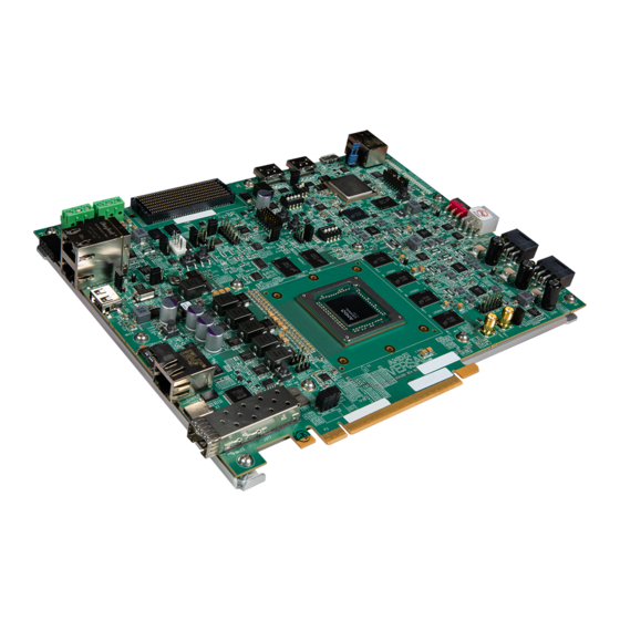
Page 10: Board Component Location
This document is not intended to be a reference design guide and the information herein should not be used as such. Always refer to the schematic, layout, and XDC files of the specific VEK280 version of interest for such details. Figure: Evaluation Board Component Locations https://docs.amd.com/internal/api/webapp/print/d54fa025-f5b0-4797-be6e-41b3e31f9548 10/78... - Page 11 J16. Connecting an ATX 6-pin connector into J16 damages the VEK280 board and voids the board warranty. Table: Board Component Locations Callout No. Ref. Des. Feature Notes Schematic Page AMD Versal™ XCVE2802-2MSELSVC4072 3-16 adaptive SoC The heatsink is not shown Figure 1 U317,...
- Page 12 Amphenol 12401598E4#2A USB Type-C FTDI FT4232HL-REEL connector (USB2.0) J308, USB 2.0 type-A Wurth 629104190121, USB connector, USB 2.0 type-A ULPI transceiver Microchip USB3320C USB 2.0 Xcvr J302, SD card socket, Molex 5025700893 U104 Versal adaptive Micro SD card cage https://docs.amd.com/internal/api/webapp/print/d54fa025-f5b0-4797-be6e-41b3e31f9548 12/78...
- Page 13 HDMI RX Conn Rcpt HDMI 2.1 RA connectors J307 GEM0 SGMII Halo HFJ11-1G01E-L12RL Ethernet PHY, RJ-45 Gigabit connector 0x01, RJ45 w/mag FMCP1 Samtec ASP-184329-01 30-34 560 pos. connector 14x40 1.27 mm Various Adaptive SoC Infineon regulators 51-56 power management https://docs.amd.com/internal/api/webapp/print/d54fa025-f5b0-4797-be6e-41b3e31f9548 13/78...
- Page 14 IC V. reg. step-down DC/DC sync U354 UTIL_1V8 regulator Infineon IR38060MTRPBF IC REG BUCK ADJ 6A U191 UTIL_3V3 regulator Infineon IR3889MTRPBFAUMA1 IC V. reg. step-down DC/DC sync U190 UTIL_5V0 regulator Infineon IR3889MTRPBFAUMA1 IC V. reg. step-down DC/DC sync https://docs.amd.com/internal/api/webapp/print/d54fa025-f5b0-4797-be6e-41b3e31f9548 14/78...
- Page 15 U297 Adaptive SoC U1 Micron OSPI MT35XU02GCBA1G12-0SIT IC flash Xccela 2 Gb SPI 200 MHz 1.8V Done LED (Active- Lumex SML-LX0603GW-TR High-Z and pulled LED green High) Error out LED Lumex SML-LX0603IW-TR (Active-High-Z and LED red pulled High) https://docs.amd.com/internal/api/webapp/print/d54fa025-f5b0-4797-be6e-41b3e31f9548 15/78...
- Page 16 CLK out SMA 400L5 Conn. rcpt. SMA vert. 50R 12.4 GHz U125 XCZU4EG system AMD XCZU4EG-2SFVC784E 73-83 controller AMD Zynq™ UltraScale+™ MPSoC U301 SYSCTLR CTS 626L15625I3T clock156.25 MHz Osc 156.25 MHz 3.3V 25 HSDP REFCLK PPM LVDS with OE U302...
-
Page 17: Default Jumper And Switch Settings
The following figure shows the VEK280 board jumper header and switch locations. Each numbered component shown in the figure is keyed to the applicable table in this section. Both tables reference the respective schematic page numbers. Figure: Board Jumper Header and Switch Locations https://docs.amd.com/internal/api/webapp/print/d54fa025-f5b0-4797-be6e-41b3e31f9548 17/78... - Page 18 Schematic Page SYSMON VREFP SEL 1-2: External VREF 2-3: Disable external VREF POR_B supervisor SENSE input 1-2: VCCO_MIO ramp-up sense (1.8V) 2-3: VCCAUX_PMC ramp-up sense (1.5V) J326 POR_B enable header 1-2, 3-4 1-2: SYSCTLR can drive POR_B jumpered https://docs.amd.com/internal/api/webapp/print/d54fa025-f5b0-4797-be6e-41b3e31f9548 18/78...
- Page 19 1-2: SYSCTLR POR_B supervisor enabled Open: SYSCTLR POR_B supervisor disabled J347 Fan type 1-2: System controller PWM 2-3: Versal device MIO PWM J348 TACH type 1-2: System controller TACH 2-3: Versal device MIO TACH J406 MIO37 selection 1-2: ZU4_TRIGGER 2-3: CANFD0_INH_B https://docs.amd.com/internal/api/webapp/print/d54fa025-f5b0-4797-be6e-41b3e31f9548 19/78...
- Page 20 VEK280 power-on reset (POR_B) Open SYSCTLR JTAG source selection OFF, ON Switch OFF = 1 = high; ON = 0 = SYSCTLR JTAG SOURCE SEL = SW3[1:2] = SEL[0:1] PL JTAG = ON,ON = 00 FTDI JTAG = OFF,ON = 10 https://docs.amd.com/internal/api/webapp/print/d54fa025-f5b0-4797-be6e-41b3e31f9548 20/78...
- Page 21 The mode DIP switch SW1 configuration option settings are listed in the following table. Table: Mode Switch SW1 Configuration Option Settings Boot Mode Mode Pins [0:3] Mode SW1 [1:4] JTAG ON, ON, ON, ON 0000 OSPI 0001 ON, ON, ON, OFF https://docs.amd.com/internal/api/webapp/print/d54fa025-f5b0-4797-be6e-41b3e31f9548 21/78...
- Page 22 (p/u to VCCO)=1. JTAG The AMD Vivado™ , AMD SDK, or third-party tools can establish a JTAG connection to the Versal device in the two ways described in this section. FTDI FT4232 USB-to-JTAG/USB-UART device (U20) connected to USB 2.0 type- C connector (J369), which requires: Set boot mode SW1 for JTAG as indicated in the "Mode Switch SW1...
- Page 23 2. Set boot MODE SW1 for SD1_3.0 as indicated in the table in Versal Device Configuration. 3. Power-cycle the VEK280 board or press the POR pushbutton SW2. SW2 is near the USB-C JTAG port J369 in the figure in Board Component Location. https://docs.amd.com/internal/api/webapp/print/d54fa025-f5b0-4797-be6e-41b3e31f9548 23/78...
-
Page 24: Board Component Descriptions
[Figure 1, callout 1] The VEK280 evaluation board is populated with the AMD Versal™ XCVE2802- 2MSEVSVH2802 device, which combines a powerful processing system (PS) and programmable logic (PL) in the same device. The PS in a Versal device features the Arm®... - Page 25 0.46V over temperature per fixed 5 mA load, R1725, and limiting 1.56V max at the device pin, PSVBATT. The second diode and 4.7 kΩ current limit resistor allows the battery to trickle charge and prevent battery B1 from back powering R1725. https://docs.amd.com/internal/api/webapp/print/d54fa025-f5b0-4797-be6e-41b3e31f9548 25/78...
- Page 26 XPIO Bank VCC1V1_LP4 1.1V LPDDR4 TRIP2 CH1 XPIO Bank 1.5V LPDDR4 TRIP2 CH0/1 reset, HDMI VADJ_FMC control signals, GPIO DIP,PB0/1, SYSCTLR GPIO[0:7], SYS_CLK_1, FMCP1_LA[00:01]_CC, FMCP1_LA[02:16],FMCP_CLK0 XPIO Bank 1.5V FMCP1_SYNC_M2C/C2M, LPDDR4 VADJ_FMC TRIP3 CH0/1 reset, SYS_CLK_2, 1588_GPIO[0:5], FMCP1_REFCLK_C2M, FMCP1_LA[17:18]_CC, https://docs.amd.com/internal/api/webapp/print/d54fa025-f5b0-4797-be6e-41b3e31f9548 26/78...
- Page 27 LPD MIO[23]: VADJ_FMC Power Rail for more details. LPDDR4 Component Memory [Figure 1, callout 2, 3, 4] The VEK280 XCVE2802 device PL DDR memory interface performance is documented in the Versal Premium Series Data Sheet: DC and AC Switching https://docs.amd.com/internal/api/webapp/print/d54fa025-f5b0-4797-be6e-41b3e31f9548 27/78...
- Page 28 XPIO triplet 1 (banks 700/701/702) XPIO triplet 2 (banks 703/704/705) XPIO triplet 3 (banks 706/707/708) Each support two independent 32-bit 2 GB component interfaces (4 GB per triplet). The VEK280 evaluation board uses the LPDDR4 memory components as follows: https://docs.amd.com/internal/api/webapp/print/d54fa025-f5b0-4797-be6e-41b3e31f9548 28/78...
- Page 29 The VEK280 board POR circuit is shown in the following figure. U235 allows directional open drain level shifting for all of these masters, and J326 allows them to be bused together if desired. The TPS389001 U10 supervisor chip holds POR_B off until power is valid. Figure: POR_B Reset Circuit https://docs.amd.com/internal/api/webapp/print/d54fa025-f5b0-4797-be6e-41b3e31f9548 29/78...
- Page 30 VEK280 evaluation board. See the Versal Adaptive SoC Technical Reference Manual (AM011) for more information on MIO peripheral mapping. Additional signal connectivity can be located in the following schematic sections: Bank 500: See schematic page 10 Bank 501: See schematic page 10 Bank 502: See schematic page 11 https://docs.amd.com/internal/api/webapp/print/d54fa025-f5b0-4797-be6e-41b3e31f9548 30/78...
- Page 31 Signal Notes OSPI PMC_MIO0_OSPI_CLK PMC_MIO1_OSPI_DQ0 PMC_MIO2_OSPI_DQ1 PMC_MIO3_OSPI_DQ2 PMC_MIO4_OSPI_DQ3 PMC_MIO5_OSPI_DQ4 PMC_MIO6_OSPI_DQS PMC_MIO7_OSPI_DQ5 PMC_MIO8_OSPI_DQ6 PMC_MIO9_OSPI_DQ7 PMC_MIO10_OSPI0_CS_BO Regulator PMC_MIO11_VCC_AUX_1V2_EN Table 1 Enable GPIO OSPI PMC_MIO12_OSPI_RST_BO PMC_MIO13_USB_RST_B O PMC_MIO14_USB_DAT0 I/O PMC_MIO15_USB_DAT1 I/O PMC_MIO16_USB_DAT2 I/O PMC_MIO17_USB_DAT3 I/O https://docs.amd.com/internal/api/webapp/print/d54fa025-f5b0-4797-be6e-41b3e31f9548 31/78...
- Page 32 PMC_MIO25_USB_NXT PMC_MIO26_SD_CLK PMC_MIO27_SD_DIR1 PMC_MIO28_SD_DET PMC_MIO29_SD_CMD PMC_MIO30_SD_DAT0 PMC_MIO31_SD_DAT1 PMC_MIO32_SD_DAT2 PMC_MIO33_SD_DAT3 PMC_MIO34_SD_SEL PMC_MIO35_SD_DIR_CMD O PMC_MIO36_SD_DIR0 Factory/CANFD0 PMC_MIO37_COMBINED I/O Selectable J406, Factory/CANFD0_INH_B Interface CANFD0 PMC_MIO38_CAN0_nSTBO Standby mode control input https://docs.amd.com/internal/api/webapp/print/d54fa025-f5b0-4797-be6e-41b3e31f9548 32/78...
- Page 33 GEM0 PMC_MIO48_GEM_RST_BO Regulator PMC_MIO49_VCC_PSLP_EN Table 1 Enable GPIO PCIe PMC_MIO50_PCIE_WAKE_B O PMC_MIO51_SD_BUSPWR O GEM0 LPD_MIO0_GEM_TX_CLK O LPD_MIO1_GEM_TX_D0 I/O LPD_MIO2_GEM_TX_D1 I/O LPD_MIO3_GEM_TX_D2 I/O LPD_MIO4_GEM_TX_D3 I/O LPD_MIO5_GEM_TX_CTL I/O LPD_MIO6_GEM_RX_CLK I https://docs.amd.com/internal/api/webapp/print/d54fa025-f5b0-4797-be6e-41b3e31f9548 33/78...
- Page 34 LPD_MIO15_CANFD0_TX O Interface CANFD1 LPD_MIO16_CANFD1_TX O LPD_MIO17_CANFD1_RX I Interface PCIe PCIE_PERST_B PCIE_PERST_B Regulator LPD_MIO20_VCC_PL_EN O Table 1 Enable GPIO MIO21_FAN_PWM_VERSAL O Versal device fan MIO22_FAN_TACH_VERSAL I Versal device fan tach Regulator LPD_MIO23_VADJ_FMC_EN VADJ_FMC enable Enable https://docs.amd.com/internal/api/webapp/print/d54fa025-f5b0-4797-be6e-41b3e31f9548 34/78...
- Page 35 The USB3320 is clocked by a 24 MHz crystal (X8). See the Standard Microsystems Corporation (SMSC) USB3320 data sheet for clocking mode details. The interface to the USB3320 PHY is implemented through the IP in the XCVE2802 device PS. https://docs.amd.com/internal/api/webapp/print/d54fa025-f5b0-4797-be6e-41b3e31f9548 35/78...
- Page 36 Settings). The USB shield can optionally be connected through a series capacitor to GND by installing a capacitor (body size 0402) at location C2762 and inserting a jumper across pins 2-3 on header J300. Figure: USB3320 USB2.0 Connector J308 Shield Connection Options https://docs.amd.com/internal/api/webapp/print/d54fa025-f5b0-4797-be6e-41b3e31f9548 36/78...
- Page 37 Unofficial Document PMC MIO[26:36, 51] Bank 501: Secure Digital (SD) Card IF [Figure 1, callout 11] The VEK280 evaluation board includes a secure digital input/output (SDIO) interface to provide access to general purpose non-volatile SDIO memory cards and https://docs.amd.com/internal/api/webapp/print/d54fa025-f5b0-4797-be6e-41b3e31f9548 37/78...
- Page 38 VEK280 evaluation board. Figure: SD Card Interface Connections The following table lists the NVT4857UK U104 adapter pinout. Table: NVT4857UK U104 Adapter Pinout Aries Adapter Pin Number NVT4857UKAZ Pin NumberNVT4857UKAZ Pin Name CLKA C3, C2 CMDA CLK_FB Unused Unused VCCB https://docs.amd.com/internal/api/webapp/print/d54fa025-f5b0-4797-be6e-41b3e31f9548 38/78...
- Page 39 CMDB DAT3B DAT2B Unused Unused The Versal device (U1) also has control over the power for the SDCARD, which allows the Versal device to remove power to the SD card as needed. Figure: SD Socket J302 Power Control https://docs.amd.com/internal/api/webapp/print/d54fa025-f5b0-4797-be6e-41b3e31f9548 39/78...
- Page 40 Versal device and an input to the CAN transceiver. PMC MIO[39:41] System Monitor I2C The Versal device PS bank 501 MIO39 (PMC_MIO39_SYSMON_I2C_SCL), MIO40 (PMC_MIO40_SYSMON_I2C_SDA), and MIO41 (PMC_MIO41_SYSMON_I2C_ALERT) are connected to the system controller for use with the system controller related applications and alerts. https://docs.amd.com/internal/api/webapp/print/d54fa025-f5b0-4797-be6e-41b3e31f9548 40/78...
- Page 41 The FTDI configuration image can be programmed with the Vivado tools. See the Programming FTDI Devices for Vivado Hardware Manager Support section in the Vivado Design Suite User Guide: Programming and Debugging (UG908). Alternatively, a JTAG-SMT2 or similar from Digilent is recommended. https://docs.amd.com/internal/api/webapp/print/d54fa025-f5b0-4797-be6e-41b3e31f9548 41/78...
- Page 42 FMCP connector, and power system status inputs and outputs. Bus I2C0 also provides access to power system PMBus power controllers and INA226 power monitors, as well as RC21008A clock components via the U33 TCA9548A switch. TCA6416A U233 is pin-strapped to respond to I2C address 0x20. The TCA9548A https://docs.amd.com/internal/api/webapp/print/d54fa025-f5b0-4797-be6e-41b3e31f9548 42/78...
- Page 43 The devices on each port of the I2C0 U233 TCA6416A port expander and on each bus of the I2C0 U33 TCA9548A switch are listed in the following tables. Table: I2C0 Port Expander TCA6416A U233 Address 0x20 Connections I2C0 Port Expander TCA6416A U233 Address 0x20 Connections I2C Devices Port Direction Device P00-P01 https://docs.amd.com/internal/api/webapp/print/d54fa025-f5b0-4797-be6e-41b3e31f9548 43/78...
- Page 44 U260, U355, U356 Table: I2C0 Multiplexer TCA9548A U33 Address 0x74 Connections I2C Devices I2C Switch Pos. I2C Address Devices PMBUS See Schematic, PMBus Regulators Map PMBUS1_INA226 See Schematic, PMBus Regulators Map No connect PMBUS2_INA226 See Schematic, PMBus Regulators Map https://docs.amd.com/internal/api/webapp/print/d54fa025-f5b0-4797-be6e-41b3e31f9548 44/78...
- Page 45 (SW15) and PMC_MIO signals as shown in the following figure. The POR_B signal generated by the TPS389001DSER U10 POR device is wired in parallel to each Ethernet PHY reset circuit. The POR device is activated by pushbutton SW2. See System Reset POR_B for more details. https://docs.amd.com/internal/api/webapp/print/d54fa025-f5b0-4797-be6e-41b3e31f9548 45/78...
- Page 46 LEDCR1[7:4] register bits. The LINK_ST pin is a general-purpose output used to indicate to the MAC whether a valid link has been established. LED_0 By default, this pin indicates that link is established. Additional functionality is configurable using LEDCR1[3:0] register bits. https://docs.amd.com/internal/api/webapp/print/d54fa025-f5b0-4797-be6e-41b3e31f9548 46/78...
- Page 47 When not installed, the Versal device shares control with UTIL_5V0_PGOOD, which is an output from the 5.0V power supply (U191). See schematic page 71 for more information (see Jumpers for defaults). Table: PMC MIO[49] and LPD MIO[12,13,20,23] Power Domains Versal Device Pin Signal Power Domains https://docs.amd.com/internal/api/webapp/print/d54fa025-f5b0-4797-be6e-41b3e31f9548 47/78...
- Page 48 The VITA 57.4 FMC+ Industry Standard calls out not only specific connectors, but behaviors of the devices being connected. This creates a highly adaptable and flexible interface allowing a best fit for many industries and prototyping needs. While AMD strives to adhere to all standards providing customers with the best https://docs.amd.com/internal/api/webapp/print/d54fa025-f5b0-4797-be6e-41b3e31f9548 48/78...
- Page 49 1, callout 14, 16] The JTAG chain includes: J36 2x7 2 mm shrouded, keyed JTAG pod flat cable connector J369 USB3 type-C connector connected to U20 FT4232HL USB-JTAG bridge U125 XCZU4EG System Controller bank 44 Figure: JTAG Chain Block Diagram https://docs.amd.com/internal/api/webapp/print/d54fa025-f5b0-4797-be6e-41b3e31f9548 49/78...
-
Page 50: Clock Generation
The VEK280 board provides fixed and variable clock sources for the XCVE2802 U1 device and other function blocks. The following table lists the source devices for each clock. Table: Clock Sources Ref. Des. Feature Notes Schematic Page U299 DDR4 DIMM CLK, 200 MHz, 3.3V LVDS, Renesas output 0x09 1RC21008A https://docs.amd.com/internal/api/webapp/print/d54fa025-f5b0-4797-be6e-41b3e31f9548 50/78... - Page 51 Adaptive SoC 3, 92 XCVE2802 The detailed device connections for the feature described in this section are documented in the VEK280 board XDC file, referenced in Xilinx Design Constraints. Programmable MGT RC21008A REF Clocks [Figure 1, callout 36] https://docs.amd.com/internal/api/webapp/print/d54fa025-f5b0-4797-be6e-41b3e31f9548 51/78...
- Page 52 The Versal device has 32 PL GTYP transceivers. The following table contains the mapping to hardened features, quads, channel locations, as well as general features. Table: Transceiver Mapping XCVE2802 FMC+ FMCP1_DP4 CH0 GTYP PCIe PCIe GTYP CH0 Versal_HSDP HSDP/ Quad X1Y2 X0Y2 Quad SFP28 https://docs.amd.com/internal/api/webapp/print/d54fa025-f5b0-4797-be6e-41b3e31f9548 52/78...
- Page 53 REF1[UNUSED] HDMI HDMI_CH0CH0 GTYP MRMAC GTYP CH0 PCIe Quad X0Y1 (CPM5) Lane7 Quad HDMI_CH1CH1 CH1 PCIe X1Y2 Lane6 CA [L] X0Y2 BC [RS] HDMI_CH2CH2 CH2 PCIe Lane5 HDMI_TX_CLK_C CH3 PCIe Lane4 HDMI_RX_CLK_C HDMI_RCLK_OUT_C REF0 REF0PCIe_CLK1 HDMI_8T49N241_OUT_C REF1 REF1[UNUSED] https://docs.amd.com/internal/api/webapp/print/d54fa025-f5b0-4797-be6e-41b3e31f9548 53/78...
- Page 54 CH0 PCIe X0Y0 (CPM5) Lane15 Quad CH1 PCIe Lane14 X0Y0 BA [RS] CH2 PCIe Lane13 CH3 PCIe Lane12 REF0PCIe_CLK3 REF1[UNUSED] HDIO PMCDIO LPDMIO Bank Bank Bank 401 AA HDIO PMCMIO PMCMIO/PMCDIO Bank Bank Bank 400 AB https://docs.amd.com/internal/api/webapp/print/d54fa025-f5b0-4797-be6e-41b3e31f9548 54/78...
- Page 55 The Samtec SEAF series 1.27 mm (0.050 in) pitch mates with the SEAM series connector. For more information about the SEAF series connectors, see the Samtec, Inc. website. The 560-pin FMC+ connector defined by the FMC specification (see VITA 57.4 FMCP Connector Pinouts) provides connectivity for up to: https://docs.amd.com/internal/api/webapp/print/d54fa025-f5b0-4797-be6e-41b3e31f9548 55/78...
- Page 56 The first release of the EA VEK280 board has a FRL data rate limit of 8 Gbps / lane The series capacitor-connected HDMI TX and RX data signals from TMDS1204 are routed to the VE2802 GTYP Bank 204. https://docs.amd.com/internal/api/webapp/print/d54fa025-f5b0-4797-be6e-41b3e31f9548 56/78...
- Page 57 TDMS1204 HDMI TX redriver 0x5E U344 TDMS1204 HDMI RX redriver 0x5B U362 8T49N241-994 FemtoClock 0x6C U364 M24128 EEPROM 0x50 The HDMI video and control I/O block diagram is shown in the following figure. Figure: HDMI Video and Control I/O Block Diagram https://docs.amd.com/internal/api/webapp/print/d54fa025-f5b0-4797-be6e-41b3e31f9548 57/78...
- Page 58 HDMI Source Clock The VEK280 evaluation board includes a Renesas RC21008A (U299). This chip is used to source the 400 MHz FRL/DRU clock used as the reference for driving the Versal device (U1) logic and related circuitry for HDMI. https://docs.amd.com/internal/api/webapp/print/d54fa025-f5b0-4797-be6e-41b3e31f9548 58/78...
-
Page 59: Hdmi Clock Recovery
5V connected to the HDMI receptacle. The block diagram in the following figure shows the I/O signal connections for HDMI TX and RX. A 128-Kbit EEPROM is provided for storing HDMI EDID metadata in the circuitry. Figure: HDMI SRC and SNK Control I/O Block Diagram https://docs.amd.com/internal/api/webapp/print/d54fa025-f5b0-4797-be6e-41b3e31f9548 59/78... - Page 60 The VEK280 board provides two CAN-FD buses. These can be used for prototyping and support classic CAN and CAN FD up to 8 Mbps. While many configurations are available, the design intention is for the VEK280 board to be a device on the bus. https://docs.amd.com/internal/api/webapp/print/d54fa025-f5b0-4797-be6e-41b3e31f9548 60/78...
- Page 61 CAN1 connects to a TI TCAN1043A CAN FD transceiver (U373). The output bus connects to screw terminal J393 for easy prototyping. Separate 60.4Ω resistors can be added to CAN1_CANL and CAN1_CANH using J398 and J397, respectively. See the VEK280 schematic pages 11 and 41 for details. Figure: CAN Buses https://docs.amd.com/internal/api/webapp/print/d54fa025-f5b0-4797-be6e-41b3e31f9548 61/78...
- Page 62 The following table lists the transceiver module control signals. Table: Transceiver Module Control Signals Signal Name Feature Notes Schematic Page SFP_SDA Two-wire interface data U33 I2C MUX 29, 39 SFP_SCL Two-wire interface clock U33 I2C MUX 29, 39 https://docs.amd.com/internal/api/webapp/print/d54fa025-f5b0-4797-be6e-41b3e31f9548 62/78...
- Page 63 User I/O [Figure 1, callout 17, 18 and Figure 1, callout 41] Switches for default values. The following table lists the net names, reference designators, and schematic pages for the user I/O. https://docs.amd.com/internal/api/webapp/print/d54fa025-f5b0-4797-be6e-41b3e31f9548 63/78...
- Page 64 4, 48 GPIO_DIP_3 4, 48 GPIO_LED0 3, 48 GPIO_LED1 3, 48 GPIO_LED2 3, 48 GPIO_LED3 3, 48 Power and Status LEDs [Figure 1, callout 32] The following figure shows the power and status LEDs. Figure: Power and Status LEDs https://docs.amd.com/internal/api/webapp/print/d54fa025-f5b0-4797-be6e-41b3e31f9548 64/78...
-
Page 65: Cooling Fan Connector
(acoustically quiet) when the Versal device's U1 is cool and rotates faster as the device heats up (acoustically noisy). The VEK280 board provides a fan controller bypass header J347 and J348 to permit control by the Versal device. See the Default Jumper and Switch Settings more details. Figure: 12V Fan Header https://docs.amd.com/internal/api/webapp/print/d54fa025-f5b0-4797-be6e-41b3e31f9548 65/78... -
Page 66: System Controller
If this image needs to be updated and for more information on the system controller web interface, see the Versal Evaluation Board System Controller Wiki. The web application is shown in the following figure. Figure: System Controller Web User Interface https://docs.amd.com/internal/api/webapp/print/d54fa025-f5b0-4797-be6e-41b3e31f9548 66/78... -
Page 67: Power On/Off Slide Switch
Board Power System for details on the onboard power system. ⚠ CAUTION! Do NOT plug a PC ATX power supply 6-pin connector into the VEK280 board power connector J16. The ATX 6-pin connector has a different pinout than https://docs.amd.com/internal/api/webapp/print/d54fa025-f5b0-4797-be6e-41b3e31f9548 67/78... -
Page 68: Board Power System
VEK280 board schematic. Table: Power System - PMBus Regulators and INA226 Map Rail Rail Name Nominal Voltage (V) Max Current (A)Device PMBUS Addr INA226 Addr VCCINT 0.80 U152 L1, U154, 0x46 0x40 U155, U157, U159, BUS1 https://docs.amd.com/internal/api/webapp/print/d54fa025-f5b0-4797-be6e-41b3e31f9548 68/78... - Page 69 0x48 0x45 BUS2 VCCO_502 1.80 U175 B 0x4D 0x47 BUS2 VCC1V1_LP4 1.10 U279 A, U292 0x48 0x49 BUS2 VCC1V5 1.50 U279 B 0x48 0x43 BUS2 VADJ_FMC 1.50 U282 0x4E 0x4A BUS2 LPDMGTYAVCC 0.92 U279 C 0x48 0x4B BUS2 https://docs.amd.com/internal/api/webapp/print/d54fa025-f5b0-4797-be6e-41b3e31f9548 69/78...
- Page 70 Infineon Integrated Circuits website. The PCB layout and power system design meet the recommended criteria described in the Versal Adaptive SoC PCB Design User Guide (UG863). Table: Power System – Non-PMBus Regulators https://docs.amd.com/internal/api/webapp/print/d54fa025-f5b0-4797-be6e-41b3e31f9548 70/78...
-
Page 71: Monitoring Voltage And Current
For connectivity details, see the schematic, which can be accessed through the VEK280 Evaluation Board website. These power system components are also accessible to the ZU4 U125 system controller (bank 501) and the Versal device U1 (bank 501). https://docs.amd.com/internal/api/webapp/print/d54fa025-f5b0-4797-be6e-41b3e31f9548 71/78... -
Page 72: Xilinx Design Constraints
RTL. See the Vivado Design Suite User Guide: Using Constraints (UG903) for more information. The HSPC FMCP connector J51 is connected to the AMD Versal™ device U1 banks powered by the variable voltage VADJ_FMC. Because different FMC cards https://docs.amd.com/internal/api/webapp/print/d54fa025-f5b0-4797-be6e-41b3e31f9548... -
Page 73: Regulatory And Compliance Information
EN 55024:2010, Information Technology Equipment Immunity Characteristics – Limits and Methods of Measurement This is a Class A product. In a domestic environment, this product can cause radio interference, in which case the user might be required to take adequate measures. https://docs.amd.com/internal/api/webapp/print/d54fa025-f5b0-4797-be6e-41b3e31f9548 73/78... -
Page 74: Compliance Markings
AMD has met its national obligations to the EU WEEE Directive by registering in those countries to which AMD is an importer. AMD has also elected to join WEEE Compliance Schemes in some countries to help manage customer returns at end-of-life. -
Page 75: Additional Resources And Legal Notices
Additional Resources and Legal Notices Finding Additional Documentation Documentation Portal The AMD Adaptive Computing Documentation Portal is an online tool that provides robust search and navigation for documentation using your web browser. To access the Documentation Portal, go to https://docs.xilinx.com. Documentation Navigator... -
Page 76: Support Resources
3/20/24, 12:51 PM Unofficial Document Design Hubs AMD Design Hubs provide links to documentation organized by design tasks and other topics, which you can use to learn key concepts and address frequently asked questions. To access the Design Hubs: In DocNav, click the Design Hubs View tab. -
Page 77: Revision History
BIOS https://docs.amd.com/internal/api/webapp/print/d54fa025-f5b0-4797-be6e-41b3e31f9548 77/78... - Page 78 AMD to notify any person of such revisions or changes. THIS INFORMATION IS PROVIDED "AS IS." AMD MAKES NO...
Need help?
Do you have a question about the XILINX VEK280 and is the answer not in the manual?
Questions and answers