Table of Contents
Advertisement
Quick Links
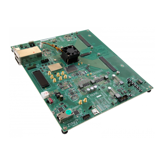
ZCU670 Evaluation Board
User Guide
UG1532 (v1.0) March 30, 2022
Xilinx is creating an environment where employees, customers, and
partners feel welcome and included. To that end, we're removing non-
inclusive language from our products and related collateral. We've
launched an internal initiative to remove language that could exclude
people or reinforce historical biases, including terms embedded in our
software and IPs. You may still find examples of non-inclusive
language in our older products as we work to make these changes and
align with evolving industry standards. Follow this
link
for more
information.
Advertisement
Table of Contents

Related Manuals for AMD Xilinx ZCU670


Summary of Contents for AMD Xilinx ZCU670
- Page 1 ZCU670 Evaluation Board User Guide UG1532 (v1.0) March 30, 2022 Xilinx is creating an environment where employees, customers, and partners feel welcome and included. To that end, we’re removing non- inclusive language from our products and related collateral. We’ve launched an internal initiative to remove language that could exclude people or reinforce historical biases, including terms embedded in our software and IPs.
-
Page 2: Table Of Contents
Table of Contents Chapter 1: Introduction ....................4 Overview............................4 Additional Resources........................4 Block Diagram..........................5 Board Features..........................5 Board Specifications........................8 Chapter 2: Board Setup and Configuration ............10 Standard ESD Measures......................10 Board Component Location.....................10 Default Jumper and Switch Settings..................14 Zynq UltraScale+ RFSoC XCZU67DR..................18 Chapter 3: Board Component Descriptions ........... - Page 3 CoreHC2 Connector Pin Out (XM755 Only)................76 Features............................77 Board Specifications......................... 79 Functional Description......................82 Appendix E: Additional Resources and Legal Notices ......92 Xilinx Resources.........................92 Documentation Navigator and Design Hubs.................92 References..........................92 Revision History......................... 94 Please Read: Important Legal Notices................... 94 UG1532 (v1.0) March 30, 2022 www.xilinx.com Send Feedback ZCU670 Board User Guide...
-
Page 4: Chapter 1: Introduction
Chapter 1: Introduction Chapter 1 Introduction Overview The ZCU670 is an evaluation board featuring the ZU67DR Zynq ® UltraScale+™ RFSoC DFE device. This board enables the evaluation of applications requiring multi-band (sub-7 GHz, mmWave), multi-std (5G, LTE, etc.), and multi-mode (TDD, FDD) radios, including Milcom and Satcom applications. -
Page 5: Block Diagram
Chapter 1: Introduction Block Diagram A block diagram of the ZCU670 evaluation board is shown in the following figure. Figure 1: Evaluation Board Block Diagram SD3.0 CPU_RESET PS_PMU_GPO[0:5] 8A34001 CLK in x1 PS PB/LED MPS430_GPIO PMU_INPUT Si5381 CLKO x1 UART0 8A34001 CLKO x1 PS_GPIO1 Si5381 CLKinx1... - Page 6 Chapter 1: Introduction Micro-SD card ○ USB-to-JTAG bridge ○ PC4 2x7 2 mm JTAG pod flat cable header ○ • Clocks SI5381 (various frequencies) ○ For additional details on this clock, see Table Table 18, and SI5381A 10 Independent Output Any-Frequency Clock Generator U43.
- Page 7 Chapter 1: Introduction • PS GTR (bank 505) assignment USB3 (1 GTR) ○ FMCP HSPC DP (3 GTR) ○ • PL GTY assignment (2 quads, 8 total GTY) 2x2 zSFP+ (4 GTY on bank GTY127) ○ FMCP HSPC DP (4 GTY, bank GTY128) ○...
-
Page 8: Board Specifications
Chapter 1: Introduction The ZCU670 provides a rapid prototyping platform that uses the XCZU67DR-2FSVE1156I device. The ZU67DR contains many useful processor system (PS) hard block peripherals exposed through the multi-use I/O (MIO) interface and a variety of FPGA programmable logic. The following table lists a brief summary of the resources available within the ZU67DR. - Page 9 Chapter 1: Introduction See the ZCU670 Evaluation Board website for the XDC listing and board schematics. Environmental Note: The operating temperature range is not fully tested across the specified temperature range. It is for general guidelines only. Customers should use the ZCU670 evaluation board for evaluation purposes only in a normal lab environment and should not operate beyond room temperature.
-
Page 10: Chapter 2: Board Setup And Configuration
Chapter 2: Board Setup and Configuration Chapter 2 Board Setup and Configuration Standard ESD Measures CAUTION! ESD can damage electronic components when they are improperly handled, and can result in total or intermittent failures. Always follow ESD-prevention procedures when removing and replacing components. - Page 11 Chapter 2: Board Setup and Configuration IMPORTANT! The following figure is for visual reference only and might not reflect the current revision of the board. IMPORTANT! There could be multiple revisions of this board. The specific details concerning the differences between revisions are not captured in this document. This document is not intended to be a reference design guide and the information herein should not be used as such.
- Page 12 Chapter 2: Board Setup and Configuration Board Component Descriptions The following table identifies the components and references the respective schematic (038-05023-01) page numbers. Table 2: ZCU670 Board Component Locations Feature Ref. Schematic Callout Notes Des. [B]=Bottom Page Zynq UltraScale+™ RFSoC fansink XCZU67DR-FFVE115 Ironwood P/N: ®...
- Page 13 Chapter 2: Board Setup and Configuration Table 2: ZCU670 Board Component Locations (cont'd) Feature Ref. Schematic Callout Notes [B]=Bottom Des. Page User pushbutton switches, active-High E-switch TL3301EP100QG SW13 CPU_RESET pushbutton, active-High E-switch TL3301EP100QG DS54- Four single color LEDs, active-High PL GPIO LEDs, LUMEX SML-LX0603GW- DS57 PS (MIO22) pushbutton E-switch TL3301EP100QG...
-
Page 14: Default Jumper And Switch Settings
Chapter 2: Board Setup and Configuration Table 2: ZCU670 Board Component Locations (cont'd) Feature Ref. Schematic Callout Notes [B]=Bottom Des. Page U118 DAC AVTT regulator [B] MPS MPM3833C Default Jumper and Switch Settings The following figure shows the ZCU670 board jumper header and switch locations. Each numbered component shown in the figure is keyed to the applicable table in this section. - Page 15 Chapter 2: Board Setup and Configuration Figure 3: Board Jumper Header and Switch Locations Round callout references a component Square callout references a component on the front side of the board on the back side of the board X25710-091021 UG1532 (v1.0) March 30, 2022 www.xilinx.com Send Feedback ZCU670 Board User Guide...
- Page 16 Chapter 2: Board Setup and Configuration Jumpers The following table lists the default jumper settings. Table 3: Default Jumper Settings Reference Schematic Callout Function Default Design Page POR_OVERRIDE 1-2: Enable 2-3: Disable SYSMON I2C Address OFF: SYSMON_VP_R floating ON: SYSMON_VP_P pulled down SYSMON I2C Address OFF: SYSMON_VN_R floating ON: SYSMON_VP_N pulled down...
- Page 17 Chapter 2: Board Setup and Configuration Table 3: Default Jumper Settings (cont'd) Reference Schematic Callout Function Default Design Page zSFP0 J29 LT enable jumper ON: zSFP0 TX_DISABLE = GND = enabled OFF: zSFP0 TX_DISABLE = high = disabled zSFP1 J29 LL enable jumper ON: zSFP1 TX_DISABLE = GND = enabled OFF: zSFP1 TX_DISABLE = high = disabled zSFP2 J29 RT enable jumper...
-
Page 18: Zynq Ultrascale+ Rfsoc Xczu67Dr
Chapter 2: Board Setup and Configuration Zynq UltraScale+ RFSoC XCZU67DR Zynq UltraScale+ RFSoC ZU67DR uses a multi-stage boot process documented in the Boot and Configuration chapter of the Zynq UltraScale+ Device Technical Reference Manual (UG1085). Switch SW2 configuration option settings are identified in the following table. Table 5: Mode Switch SW2 Configuration Option Settings Mode Mode Pins [3:0]... - Page 19 Chapter 2: Board Setup and Configuration See the Zynq UltraScale+ Device Technical Reference Manual (UG1085) for more information about Zynq UltraScale+ RFSoC configuration options. UG1532 (v1.0) March 30, 2022 www.xilinx.com Send Feedback ZCU670 Board User Guide...
-
Page 20: Chapter 3: Board Component Descriptions
Chapter 3: Board Component Descriptions Chapter 3 Board Component Descriptions Overview This chapter provides a description of the board’s components and features. Table 2 identifies the components and references the respective schematic page numbers. Component locations are shown in Figure Component Descriptions Zynq UltraScale+ RFSoC XCZU67DR [Figure... - Page 21 Chapter 3: Board Component Descriptions Figure 4: Zynq UltraScale+ RFSoC Top-level Block Diagram Processing System Cortex-A53 Cortex-A53 Cortex-A53 Cortex-A53 32 KB I/D 32 KB I/D 32 KB I/D 32 KB I/D Cortex-R5 Cortex-R5 32 KB I/D 32 KB I/D 128 KB TCM 128 KB TCM 1 MB L2 Low Power Switch...
- Page 22 Chapter 3: Board Component Descriptions The Zynq UltraScale+ RFSoC PS block has three major processing units: • Cortex-A53 application processing unit (APU) Arm v8 architecture-based 64-bit quad-core multiprocessing CPU. • Cortex-R5F real-time processing unit (RPU) Arm v7 architecture-based 32-bit dual RPU with dedicated tightly-coupled memory (TCM).
- Page 23 Chapter 3: Board Component Descriptions Figure 5: Zynq UltraScale+ RFSoC DFE Block Diagram Clocking Prog. DUC & P/Q re- iFFT channel mixer sampler filter P/Q re- PRACH sampler filter & Prog. Complex P/Q re- Mixer channel equalizer sampler & DDC filter Adaptable Logic Fabric Processor Subsystem...
- Page 24 Chapter 3: Board Component Descriptions Figure 6: Encryption Key Battery Backup Circuit X25697-090221 The Seiko TS621E rechargeable 1.5V lithium button-type battery B1 is soldered to the board with the positive output connected to the ZU67DR RFSoC U1 VCC_PSBATT pin AE29. The battery supply current IBATT specification is 150 nA maximum when board power is off.
- Page 25 Chapter 3: Board Component Descriptions Table 6: I/O Voltage Rails (cont'd) Power Net ZU67DR Voltage Connected To Name PS Bank 504 VCC1V2 1.2V PS_DDR4_SODIMM (64-BIT) I/F PS DDR4 SODIMM Socket [Figure 2, callout 2] The PS-side memory is wired to the Zynq UltraScale+ RFSoC DDRC Bank 504 hard memory controller.
- Page 26 Chapter 3: Board Component Descriptions The 4 GB, 32-bit wide DDR4 memory system is comprised of four 1 Gb x 8 SDRAM (Micron MT40A1G8SA-075), U96-U99. This memory system is connected to PL-side ZU67DR banks 64 and 65. The DDR4 0.6V PL_DDR4_C0_VTT termination voltage is supplied from TPS51200DRCT sink-source regulator U79.
- Page 27 Chapter 3: Board Component Descriptions Table 7: MIO Peripheral Mapping (cont'd) MIO[0:25] Bank 500 MIO[26:51] Bank 501 MIO[52:77] Bank 502 QSPI_UPR PMU GPO USB0 QSPI_UPR PMU GPO USB0 QSPI_UPR PMU GPO USB0 QSPI_UPR PMU GPO USB0 QSPI_UPR PMU GPO USB0 QSPI_UPR GPIO GEM3...
- Page 28 Chapter 3: Board Component Descriptions • Data rate: Various depending on Single/Dual/Quad mode The configuration and Quad-SPI section of the Zynq UltraScale+ Device Technical Reference Manual (UG1085) provides details on using the Quad-SPI flash memory. For more QSPI details, see the Micron MT25QU02GCBB8E12-0SIT data sheet on the Micron Technology website.
- Page 29 Chapter 3: Board Component Descriptions Figure 7: I2C0 and I2C1 Bus Connectivity Overview I2C0 I2C1 System Controller EEPROM 0x74 SI5381 USER_SI570_C0 U38 MSP430 USER_MGT_S1570 Zynq UltraScale+ PS_I2C1 8A34001 PS_I2C0 RFSoc PS-Side CLK104 RFMC_2 N.C. RFSoC PL-Side U20 TCA9548A U1 XCZU67DR 0x20 0x75 MAX6643_OT_B...
- Page 30 Chapter 3: Board Component Descriptions The following figure shows a high-level view of the I2C0 bus connectivity. Figure 8: I2C0 Bus Topology TCA6416A MAX6643_OT_B MAX6643_FANFAIL_B MI026_PMU_INPUT_LS DAC_AVTT_VOUT_SEL BANK 500 SI5381_INT_ALM PS I2C0 IIC_MUX_RESET_B GEM3_EXP_RESET_B I2C0_SDA/SCL SDA/ MIO15/ MAX6643_FULL_SPEED MIO14 FMC_HSPC_PRSNT_M2C_B CLK_SPI_MUX_SEL0 CLK_SPI_MUX_SEL1 IRPS5401_ALERT_B...
- Page 31 Chapter 3: Board Component Descriptions Table 9: I2C0 Port Expander TCA6416A U15 Connections (cont'd) TCA6416A U15 Connected To Schematic Net Name Pin Name Pin Name Ref. Designator Device IIC_MUX_RESET_B RESET_B TCA9548A GEN3_EXP_RESET_B SN74LVC1G08 MAX6643_FULL_SPEED FULLSPD MAX6643 FMCP_HSPC_PRSNT_M PRSNT_M2C_L J28(H) ASP_184329_01 2C_B PRSNT_M2C_L J28(N)
- Page 32 Chapter 3: Board Component Descriptions Figure 9: I2C1 Bus Topology BANK 500 TCA9548A IIC_EEPROM_SDA/SCL SD0/SC0 PS I2C1 S15381_SDA/SCL SD1/SC1 USER_S1570__C0_SDA/SCL I2C1_SDA/SCL MIO17/ SD2/SC2 SDA/SCL MIO16 USER_MGT_S1570_SDA/SCL SD3/SC3 8A34001_SDA/SCL SD4/SC5 CLK104_SDA/SCL SD5/SC5 RFMC_I2C_SDA/SCL SD6/SC6 Not Connected SD7/SC7 0x74 MPS430 P4_1 P4_2 TCA9548A FMCP_HSPC_II_SDA/SCL SD0/SC0...
- Page 33 Chapter 3: Board Component Descriptions Table 12: I2C1 TCA9548A U22 Target Device Addresses TCA9548A U22 (Addr 0x75) Port I2C1 Bus Device Target Device Address FMCP HSPC J28 0x## USER Si570 C1 Clock U130 0X5D SYSMON U1 BANK 65 0x32 PS DDR4 SODIMM SKT. J48 0x51 SFP3 P3 0x50...
- Page 34 Chapter 3: Board Component Descriptions Figure 10: ZCU670 FT4232HL Connectivity X25702-090221 For more information on the FT4232HL, see the Future Technology Devices International Ltd. website. The detailed RFSoC connections for the feature described in this section are documented in the ZCU670 board XDC file, referenced in Appendix B: Xilinx Design Constraints.
- Page 35 Chapter 3: Board Component Descriptions PMU GPO (MIO 32-37) The platform management unit (PMU) within the Zynq UltraScale+ RFSoC signals power domain changes using the PMU output pins for deep-sleep mode. The Zynq UltraScale+ RFSoC PMU GPO pins are connected to inputs of the MSP430 system controller through the TXS0108E level- shifter U37.
- Page 36 Chapter 3: Board Component Descriptions The SDIO signals are connected to ZU67DR RFSoC PS bank 501 which has its VCCMIO set to 1.8V. The SD interface nets MIO[46:49]_SDIO_DAT[0:3], MIO50_SDIO_CMD, and MIO51_SDIO_CLK each have a series 30Ω resistor at the Bank 501 source. An NXP NVT4857UK SD 3.0-compliant voltage level-translator U23 is present between the ZU67DR RFSoC and the SD card connector (J23).
- Page 37 Chapter 3: Board Component Descriptions Table 15: NVT4857UK U23 Adapter Pinout (cont'd) Adapter Pin Number NVT4857UKAZ Pin Number NVT4857UKAZ Pin Name VCCB Unused Unused Unused Unused VCCA Unused Unused DAT0A DAT3A DAT1A Unused Unused DAT2A DAT1B DAT0B CLKB CMDB DAT3B DAT2B Unused Unused...
- Page 38 Chapter 3: Board Component Descriptions The ZCU670 board uses a Standard Microsystems Corporation USB3320 USB 2.0 ULPI Transceiver (U6) to support a USB connection to the host computer. A USB cable is supplied in the ZCU670 Evaluation Kit (standard-A connector to host computer, USB 3.0 A connector to ZCU670 board connector J18).
- Page 39 Chapter 3: Board Component Descriptions Figure 13: USB3320 ULPI USB 2.0 Transceiver Circuit X25882-101921 The detailed RFSoC connections for the feature described in this section are documented in the ZCU670 board XDC file, referenced in Appendix B: Xilinx Design Constraints. GEM3 Ethernet (MIO 64-77) [Figure 2, callout 16]...
- Page 40 Chapter 3: Board Component Descriptions 10/100/1000 MHz Tri-Speed Ethernet PHY [Figure 2, callout 16] The ZCU670 board uses the TI DP83867IRPAP Ethernet RGMII PHY (U33) (see Texas Instruments website) for Ethernet communications at 10 Mb/s, 100 Mb/s, or 1000 Mb/s. The board supports RGMII mode only.
- Page 41 Chapter 3: Board Component Descriptions Table 16: Ethernet PHY LED Functional Description (cont'd) Pin Name Type Description By default, this pin indicates that link is established. LED_0 S, I/O, PD Additional functionality is configurable by means of LEDCR1[3:0] register bits. The LED functions can be re-purposed with a LEDCR1 register write available through the PHYs management data interface, MDIO/MDC.
- Page 42 Chapter 3: Board Component Descriptions Figure 16: JTAG Chain Block Diagram JTAG 2 mm 2X7 Header FT4232HL UART BRIDGE JTAG N.C. J28 (D) JTAG FMCP HSPC Connector PS Config Bank 503 JTAG X23652-012220 Clock Generation The ZCU670 board provides fixed and variable clock sources for the ZU67DR Zynq UltraScale+ RFSoC.
- Page 43 Chapter 3: Board Component Descriptions Table 17: ZCU670 Board Clock Sources (cont'd) Clock (Net) Name Frequency Clock Source Programmable Frequency Clocks USER_SI570_C0 300 MHz (Default) U47 SI570 I2C PROG. OSC. (0x5D) USER_MGT_SI570_CLOCK 156.25 MHz (Default) U48 SI570 I2C PROG. OSC. (0x5D) BUF_GTR_REF_CLK0 –...
- Page 44 Chapter 3: Board Component Descriptions Table 18: Clock Connections to ZU67DR U1 (cont'd) Clock Source Ref. Des. and Net Name I/O Standard U43.38 SI5381_GTR_REF_CLK_P U43.37 SI5381_GTR_REF_CLK_N U43.42 SI5381_PL_CLK_P LVDS U43.41 SI5381_PL_CLK_N LVDS U43.45 SI5381_GTR_REFCLK_USB3_P U43.44 SI5381_GTR_REFCLK_USB3_N U43.51 SI5381_CLK_125_P LVDS U43.50 SI5381_CLK_125_N LVDS U43.54...
- Page 45 Chapter 3: Board Component Descriptions SI5381A 10 Independent Output Any-Frequency Clock Generator [Figure 2, callout 10] • Clock generator: Skyworks Solutions, Inc. (SiLabs) SI5381A-E13960-GMR • I2C programmable • Jitter: <72 fs RMS typical • Differential and single-ended factory default outputs The SI5381A data sheet addendum for the Skyworks Solutions, Inc.
- Page 46 Chapter 3: Board Component Descriptions OUT7: Unused ○ OUT8: 10 MHz ○ Enabled, LVCMOS (J147) ○ OUT9: Unused ○ Programmable User SI570 Clocks [Figure 2, callouts 4, 11, and 12] The ZCU670 board has three I2C programmable SI570 low-jitter 3.3V LVDS differential oscillators, one assigned to the DDR4 component memory interface bank (Bank 65 I/F C0: U47), one assigned to the PS reference clock (Bank 503 U1.M25 PS_REF_CLK), and one assigned to GTY131 (U48).
- Page 47 Chapter 3: Board Component Descriptions GTY SI570: • Programmable oscillator: Skyworks Solutions, Inc. (SiLabs) SI570BAB000544DG (10 MHz-810 MHz, 156.250 MHz default) • I2C 0x5D • LVDS differential output • Total stability: 61.5 ppm The SI5341A and SI570 data sheets can be found on the Silicon Labs website.
- Page 48 Chapter 3: Board Component Descriptions Figure 17: Quad-zSFP Connector zSFP Locations Looking at the J29 front opening: First character: L = Left, R = Right, Second character: T = Top, L = Lower SFP0 SFP2 SFP1 SFP3 X24156-062520 The detailed RFSoC connections for the feature described in this section are documented in the ZCU670 board XDC file, referenced in Appendix B: Xilinx Design Constraints.
- Page 49 Chapter 3: Board Component Descriptions Table 19: zSFP Control and Status Board Connections (cont'd) zSFP Control/ Status Signal Board Connection SFP_RS1 PU R271 / PD R274 PU R271 = Full TX bandwidth PD R274 = Reduced TX bandwidth SFP_LOS Test Point TP16 High = Loss of receiver signal Low = Normal operation SFP2 J29 RT...
- Page 50 Chapter 3: Board Component Descriptions • Four single color LEDs (callout 23) LED_0: DS54 ○ LED_1: DS55 ○ LED_2: DS56 ○ LED_3: DS57 ○ • One user pushbutton and a CPU reset PB switch (callouts 24 and 25) GPIO_SW_PL: SW8 ○...
- Page 51 Chapter 3: Board Component Descriptions Table 20: Power and Status LEDs (cont'd) Schematic Net Ref. Des. Description Name Color DS20 VCCINT_PG Green VCCINT 0.85VDC power On DS21 VCCINT_IO_BRAM_PS_ Green VCCPSINTFP/LP/block RAM/I/O 0.85VDC power on DS22 VCC1V8_PG Green VCC1V8 1.8VDC power on DS23 VCC1V2_PG Green...
- Page 52 Chapter 3: Board Component Descriptions Figure 18: GPIO and Power Status LED Areas X25721-090921 Multi-Gigabit Transceivers The ZU67DR Zynq UltraScale+ RFSoC has 4 GTR gigabit transceivers (6 Gb/s capable) on the PS- side and 8 GTY gigabit transceivers (28 Gb/s capable) on the PL-side. All 4 GTR and all 8 GTY transceivers are allocated.
- Page 53 Chapter 3: Board Component Descriptions GTY Transceivers The GTY transceivers in the ZU67DR are grouped into two channels or quads. The reference clock for a quad can be sourced from the quad above or the quad below the GTY quad of interest.
- Page 54 Chapter 3: Board Component Descriptions Bank 505 lanes 0, 1, and 3 support FMC+ over J28. Bank 505 reference clocks are connected to the U43 SI5341A clock generator as described in SI5381A 10 Independent Output Any-Frequency Clock Generator U43. The detailed RFSoC connections for the feature described in this section are documented in the ZCU670 board XDC file, referenced in Appendix B: Xilinx Design Constraints.
- Page 55 Chapter 3: Board Component Descriptions See the FPGA Mezzanine Card (FMC) VITA 57.4 specification on the VITA FMC Marketing Alliance website for additional information on the FMCP HSPC connector. The detailed RFSoC connections for the feature described in this section are documented in the ZCU670 board XDC file, referenced in Appendix B: Xilinx Design Constraints.
- Page 56 Chapter 3: Board Component Descriptions At power on, the system controller detects if an FMC module is installed on J28: • If no card is attached to the FMCP connector, the VADJ voltage is set to 1.8V. • When an FMC card is attached, its IIC EEPROM is read to find a VADJ voltage supported by both the ZCU670 board and the FMC module, within the available choices of 0.0V, 1.2V, 1.5V, and 1.8V.
- Page 57 Chapter 3: Board Component Descriptions 6. Launch the board user interface application. On first use of the board user interface, go to the FMC → Set VADJ → Boot-up tab and click USE FMC EEPROM Voltage. The board user interface buttons gray out during command execution and return to their original appearance when ready to accept a new command.
- Page 58 Chapter 3: Board Component Descriptions CAUTION! Do NOT plug a PC ATX power supply 6-pin connector into the ZCU670 board power connector J50. The ATX 6-pin connector has a different pinout than J50. Connecting an ATX 6-pin connector into J50 damages the ZCU670 board and voids the board warranty. The following figure shows the power connector J50, power switch SW2, and LED indicator DS19.
- Page 59 Chapter 3: Board Component Descriptions Figure 21: POR_B SW4 and PS SRST_B SW5 Pushbutton Switches X25886-101921 PS_POR_B Reset Depressing and then releasing pushbutton SW4 causes net PS_POR_B to strobe Low. This reset is used to hold the PS in reset until all PS power supplies are at the required voltage levels. It must be held Low through PS power-up.
- Page 60 Chapter 3: Board Component Descriptions Table 22: ZCU670 Power System Devices INA226 INA226 Ref. Des., PMBUS Controller or Voltage Max. Sense Schem. Rail Name Power PMBUS ADDR Regulator Current (A) Resistor (Ω) Page Monitor ADDR IR35215_PWM1/2 0.85 0x40 R440: 0.0005 CCINT PMIC1 U104 (0X40) IR35215_PWM1_L2...
- Page 61 Chapter 3: Board Component Descriptions Table 23: Device Rail Maximum Current Device Rail Maximum Current (Amps) CCINT CCINT_IO CCBRAM CC_PSINTLP CC_PSINTFP CC_PSINTFP_DDR MGTYV CCAUX PS_MGTRAVTT MGTYA PS_MGTRAVCC MGTYA CC_PSPLL CCINT_AMS ADC_AVCC ADC_AVCCAUX DAC_AVCC DAC_AVCCAUX DAC_AVTT 1.8V + V CCAUX CCAUX_IO CCAUX_IO CC_PSAUX CC_PSDDR_PLL...
- Page 62 Chapter 3: Board Component Descriptions As described in I2C0 (MIO 14-15), the I2C0 bus provides access to the PMBus power controllers and the INA226 power monitors through the U17 PCA9544A bus switch. All PMBus controlled Infineon regulators are tied to the IRPS5401_SDA/SCL PMBUS, while the INA226 power monitors are separated on to INA226_PMBUS.
-
Page 63: Appendix A: Vita57.4 Fmcp Connector Pinout
Appendix A: VITA57.4 FMCP Connector Pinout Appendix A VITA57.4 FMCP Connector Pinout The following figure shows the pinout of the FPGA plus mezzanine card (FMCP) high pin count (HSPC) connector defined by the VITA 57.4 FMC specification. For a description of how the ZCU670 evaluation board implements the FMCP specification, see FPGA Mezzanine Card Interface. -
Page 64: Appendix B: Xilinx Design Constraints
Appendix B: Xilinx Design Constraints Appendix B Xilinx Design Constraints Overview The Xilinx design constraints (XDC) file template for the ZCU670 board provides for designs targeting the ZCU670 evaluation board. Net names in the constraints listed correlate with net names on the latest ZCU670 evaluation board schematic. Identify the appropriate pins and replace the net names with net names in the user RTL. -
Page 65: Appendix C: Regulatory And Compliance Information
Appendix C: Regulatory and Compliance Information Appendix C Regulatory and Compliance Information This product is designed and tested to conform to the European Union directives and standards described in this section. For Technical Support, open a Support Service Request. CE Information CE Directives 2006/95/EC, Low Voltage Directive (LVD) 2004/108/EC, Electromagnetic Compatibility (EMC) Directive... -
Page 66: Compliance Markings
Appendix C: Regulatory and Compliance Information Compliance Markings In August of 2005, the European Union (EU) implemented the EU Waste Electrical and Electronic Equipment (WEEE) Directive 2002/96/EC and later the WEEE Recast Directive 2012/19/EU. These directives require Producers of electronic and electrical equipment (EEE) to manage and finance the collection, reuse, recycling and to appropriately treat WEEE that the Producer places on the EU market after August 13, 2005. -
Page 67: Appendix D: Hw-Xm650/755 Balun Daughter Cards For Rfsoc Evm
Appendix D: HW-XM650/755 Balun Daughter Cards for RFSoC EVM Appendix D HW-XM650/755 Balun Daughter Cards for RFSoC EVM Overview XM650 and XM755 are the RFMC 2.0 add-on cards for use with the Zynq ® UltraScale+™ RFSoC DFE ZCU670 evaluation board. These add-on cards enable ZCU670 connectivity from DAC and ADC for loopback evaluation and for instrumentation use cases. -
Page 68: Block Diagram
Appendix D: HW-XM650/755 Balun Daughter Cards for RFSoC EVM Block Diagram XM755: 16T16R Breakout Add-on Card Figure 23: XM755 Block Diagram XM650: 16T16R N79 Band Loopback Demo Add-on Card Figure 24: XM650 Block Diagram UG1532 (v1.0) March 30, 2022 www.xilinx.com Send Feedback ZCU670 Board User Guide... -
Page 69: Connector
Appendix D: HW-XM650/755 Balun Daughter Cards for RFSoC EVM Connector Table 25: RFMC 2.0 Connector Parameters Parameter Value Part number LPAM-50-01.0-L-08-2-K-TR Data rate 18 Gb/s Connector type LP array (.050"/1.27 mm pitch) I/O pins 8x50 Stack height .157"/4.00 mm (Mated with LPAF-50-03.0-L-08-2-K-TR) Make SAMTEC Description... - Page 70 Appendix D: HW-XM650/755 Balun Daughter Cards for RFSoC EVM Figure 26: LPAM Connector Drawing UG1532 (v1.0) March 30, 2022 www.xilinx.com Send Feedback ZCU670 Board User Guide...
-
Page 71: Xm650/755 Connector Pinouts
Appendix D: HW-XM650/755 Balun Daughter Cards for RFSoC EVM XM650/755 Connector Pinouts The following table lists the connector pinouts for XM650/755. Table 26: Connector Pinouts J55 DAC DACIO_VADJ DACIO_VADJ DAC_AVTT Spare 1 DACIO_00 DACIO_04 DACIO_08 DACIO_12 DACIO_02 DACIO_06 DACIO_10 DACIO_14 DACIO_01 DACIO_05 DACIO_09... - Page 72 Appendix D: HW-XM650/755 Balun Daughter Cards for RFSoC EVM Table 26: Connector Pinouts (cont'd) J55 DAC DAC_T1_CH1_N DAC_T1_CH1_P DAC_T1_CH0_N DAC_T1_CH0_P DAC_T0_CH3_N DAC_T0_CH3_P DAC_T0_CH2_N DAC_T0_CH2_P DAC_T0_CH1_N DAC_T0_CH1_P DAC_T0_CH0_N DAC_T0_CH0_P UG1532 (v1.0) March 30, 2022 www.xilinx.com Send Feedback ZCU670 Board User Guide...
- Page 73 Appendix D: HW-XM650/755 Balun Daughter Cards for RFSoC EVM Table 26: Connector Pinouts (cont'd) J55 DAC Table 27: Connector Pinouts J49 ADC ADC_T2_CH ADC_T2_CH 23_N 23_P ADC_T1_CH ADC_T1_CH ADC_T2_CH ADC_T2_CH 01_N 01_P ADC_T1_CH ADC_T1_CH ADC_T1_CH ADC_T1_CH UG1532 (v1.0) March 30, 2022 www.xilinx.com Send Feedback ZCU670 Board User Guide...
- Page 74 Appendix D: HW-XM650/755 Balun Daughter Cards for RFSoC EVM Table 27: Connector Pinouts (cont'd) J49 ADC ADC_T1_CH ADC_T1_CH ADC_T0_CH ADC_T0_CH ADC_T0_CH ADC_T0_CH ADC_T0_CH ADC_T0_CH ADC_T0_CH ADC_T0_CH UG1532 (v1.0) March 30, 2022 www.xilinx.com Send Feedback ZCU670 Board User Guide...
- Page 75 Appendix D: HW-XM650/755 Balun Daughter Cards for RFSoC EVM Table 27: Connector Pinouts (cont'd) J49 ADC VCM_ADC_T VCM_ADC_T VCM_ADC_T VCM_ADC_T 0_CH23 1_CH23 2_CH23 3_CH23 VCM_ADC_T VCM_ADC_T VCM_ADC_T VCM_ADC_T 0_CH01 1_CH01 2_CH01 3_CH01 ADCIO_02 ADCIO_06 ADCIO_10 ADCIO_14 ADCIO_00 ADCIO_04 ADCIO_08 ADCIO_12 ADCIO_03 ADCIO_07 ADCIO_11...
-
Page 76: Corehc2 Connector Pin Out (Xm755 Only)
Appendix D: HW-XM650/755 Balun Daughter Cards for RFSoC EVM CoreHC2 Connector Pin Out (XM755 Only) Figure 27: ADC: Eight Receiver Signal Lanes Plus Two Observation Lanes JHC5 JHC6 ADC_T0_CH0 ADC_T0_CH1 Tile Channel ADC_T0_CH2 ADC_T0_CH3 ADC_T1_CH0 ADC_T1_CH1 ADC_T1_CH2 ADC_T2_CH01 ADC_T1_CH3 ADC_T2_CH23 JHC7 JHC8 X25992-112321... -
Page 77: Features
Appendix D: HW-XM650/755 Balun Daughter Cards for RFSoC EVM Figure 28: DAC: Eight Transmitter Signal Lanes JHC1 JHC2 DAC_T0_CH0 DAC_T0_CH1 Tile Channel DAC_T0_CH2 DAC_T0_CH3 DAC_T1_CH0 DAC_T1_CH1 DAC_T1_CH2 DAC_T1_CH3 JHC3 JHC4 X25995-112321 Note: For ZCU670-specific mapping, see XM755 to ZCU670 Signal Mapping (XTP719). Features The XM755 balun add-on card uses the 8 x 50 x 2 female LPAM-50-01.0-L-08-2-K-TR connectors and pinout as defined in... - Page 78 Appendix D: HW-XM650/755 Balun Daughter Cards for RFSoC EVM • 2 ADC inputs – compression mount SMAs through mid frequency baluns – Anaren BD1631J50100AHF • 2 ADC inputs – compression mount SMAs through high frequency baluns – Anaren BD3150N50100AHF • 2 ADC inputs - compression mount SMAs through high freq baluns – Anaren BD60120N50100AHF •...
-
Page 79: Board Specifications
Appendix D: HW-XM650/755 Balun Daughter Cards for RFSoC EVM Board Specifications Board Dimensions/Form Factor When the module is mated with ZCU670 RFMC 2.0 connectors (Samtec LPAF-50-03.0-L-08-2- K-TR), the mated height between the boards will be 4.0 mm. No component is placed on the bottom side of the module. - Page 80 Appendix D: HW-XM650/755 Balun Daughter Cards for RFSoC EVM Figure 29: XM755 Board Dimensions • XM650 Dimensions: Length: 9.85" (250.19 mm) UG1532 (v1.0) March 30, 2022 www.xilinx.com Send Feedback ZCU670 Board User Guide...
- Page 81 Appendix D: HW-XM650/755 Balun Daughter Cards for RFSoC EVM Width: 2.65" (67.31 mm) Thickness: 0.065" (1.651 mm) Figure 30: XM650 Board Dimensions Mounting Holes/Keepouts There are four jack screws on the module and two edge standoff, as shown in the figure above. The boards are screwed to the ZCU670 board.
-
Page 82: Functional Description
Appendix D: HW-XM650/755 Balun Daughter Cards for RFSoC EVM Table 28: Mounting Screws and Standoff Details Parameters Screw Standoff Part number JSO-0415-01 Keystone 1894 Length 4 mm board stack height 0.625" + rubber bumper Ordering part number JSO-0415-01 1894 Description Jack screw press-in standoff #4-40 0.625"... - Page 83 Appendix D: HW-XM650/755 Balun Daughter Cards for RFSoC EVM Figure 32: TM40-0157-00 Landing Pad O .085[2.150] O .012+001[0:] 070± 0.025 .530± 0.013 .016[0.411] .031[0.790] .024[0.600] .024[0.600] .078[1.986] X23659-041420 SMAs: Carlisle Compression – Mount SMA, TMB-V5F2-1L1 UG1532 (v1.0) March 30, 2022 www.xilinx.com Send Feedback ZCU670 Board User Guide...
- Page 84 Appendix D: HW-XM650/755 Balun Daughter Cards for RFSoC EVM Figure 33: TMB-V5F2-1L1 SMA Drawing Figure 34: SMA to SMA Cable: Carlisle TM40-0159-00 6" UG1532 (v1.0) March 30, 2022 www.xilinx.com Send Feedback ZCU670 Board User Guide...
- Page 85 Appendix D: HW-XM650/755 Balun Daughter Cards for RFSoC EVM Balun/Filter XM755 Table 29: Low Frequency Balun Part Number Parameter Value Part number TCM2-33WX+ Manufacturer Minicircuits Order P/N TCM2-33WX+ Vendor Minicircuits Description 10 to 3000 MHz RF transformer Data sheet See the Minicircuits website Table 30: Low Frequency Balun Specifications - Electrical Specifications at 25°...
- Page 86 Appendix D: HW-XM650/755 Balun Daughter Cards for RFSoC EVM Figure 35: Low Frequency Balun Drawing MODEL MARKING (ORIENTATION) D TYP C MAX E TYP COMPONENT AREA F TYP G TYP SEE NOTE 3 IOP-HAT/PICK & PLACE SURFACE AREA PCB Land Pattern (.10x.10) MIN Total thickness: .013 inches MAX.
- Page 87 Appendix D: HW-XM650/755 Balun Daughter Cards for RFSoC EVM Figure 36: Medium Frequency Balun Specifications Figure 37: Medium Frequency Balun Drawing TOP VIEW (Near Side) SIDE VIEW BOTTOM VIEW (Far Side) 4x 0.37 2.04+0.10 0.68+0.07 2x 0.15 1.29+0.10 6x 0.98 6x 0.22 6x 0.30 Orientation Marker...
- Page 88 Appendix D: HW-XM650/755 Balun Daughter Cards for RFSoC EVM Figure 38: High Frequency Balun Specifications Figure 39: High Frequency Balun Drawing Table 34: High Frequency Balun (6-12 GHz) Part Number Parameter Value Part number BD60120N50100AHF Manufacturer Anaren Order P/N BD60120N50100AHF-ND Vendor Digikey Description...
- Page 89 Appendix D: HW-XM650/755 Balun Daughter Cards for RFSoC EVM Figure 40: High Frequency Balun Specifications Figure 41: High Frequency Balun Drawing RF Cages Table 35: RF Cages Parameter Value Part number LT-7925 Manufacturer Leader Tech Order P/N LT-7925 Vendor Leader Tech Description EMI cage UG1532 (v1.0) March 30, 2022...
- Page 90 Appendix D: HW-XM650/755 Balun Daughter Cards for RFSoC EVM Table 35: RF Cages (cont'd) Parameter Value Data sheet See the Leader Tech website XM650 Table 36: N79 Band Pass Filter Parameter Value Part number LFB184G70CT6F122TEMP Manufacturer Murata Order P/N LFB184G70CT6F122TEMP Vendor Murata Description...
- Page 91 Appendix D: HW-XM650/755 Balun Daughter Cards for RFSoC EVM Figure 42: High ADCIO and DACIO Digital I/O Header Pins UG1532 (v1.0) March 30, 2022 www.xilinx.com Send Feedback ZCU670 Board User Guide...
-
Page 92: Appendix E: Additional Resources And Legal Notices
Appendix E: Additional Resources and Legal Notices Appendix E Additional Resources and Legal Notices Xilinx Resources For support resources such as Answers, Documentation, Downloads, and Forums, see Xilinx Support. Documentation Navigator and Design Hubs Xilinx ® Documentation Navigator (DocNav) provides access to Xilinx documents, videos, and support resources, which you can filter and search to find information. - Page 93 Appendix E: Additional Resources and Legal Notices These documents provide supplemental material useful with this guide: 1. Zynq UltraScale+ RFSoC Data Sheet: Overview (DS889) 2. Zynq UltraScale+ RFSoC DFE Data Sheet: Overview (DS883) 3. Zynq UltraScale+ RFSoC Data Sheet: DC and AC Switching Characteristics (DS926) 4.
-
Page 94: Revision History
Appendix E: Additional Resources and Legal Notices Revision History The following table shows the revision history for this document. Section Revision Summary 03/30/2022 Version 1.0 Initial release. Please Read: Important Legal Notices The information disclosed to you hereunder (the "Materials") is provided solely for the selection and use of Xilinx products.
Need help?
Do you have a question about the Xilinx ZCU670 and is the answer not in the manual?
Questions and answers