Table of Contents
Advertisement
Quick Links
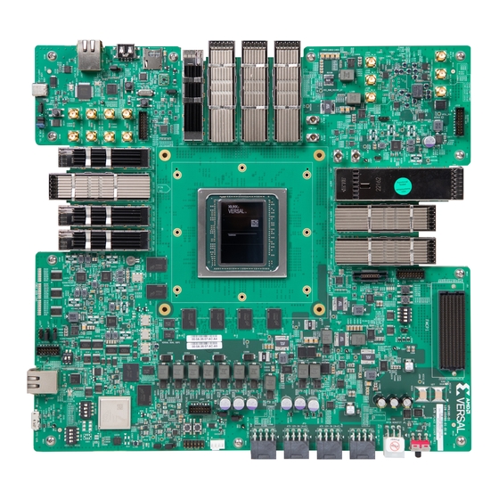
VPK180 Evaluation Board
User Guide
UG1582 (v1.0) February 21, 2023
Xilinx is creating an environment where employees, customers, and
partners feel welcome and included. To that end, we're removing non-
inclusive language from our products and related collateral. We've
launched an internal initiative to remove language that could exclude
people or reinforce historical biases, including terms embedded in our
software and IPs. You may still find examples of non-inclusive language
in our older products as we work to make these changes and align
with evolving industry standards. Follow this
link
for more
information.
Advertisement
Table of Contents

Related Manuals for AMD XILINX VPK180


Summary of Contents for AMD XILINX VPK180
- Page 1 VPK180 Evaluation Board User Guide UG1582 (v1.0) February 21, 2023 Xilinx is creating an environment where employees, customers, and partners feel welcome and included. To that end, we’re removing non- inclusive language from our products and related collateral. We’ve launched an internal initiative to remove language that could exclude people or reinforce historical biases, including terms embedded in our software and IPs.
-
Page 2: Table Of Contents
Table of Contents Chapter 1: Introduction ....................4 Overview............................4 Navigating Content by Design Process..................5 Additional Resources........................5 Block Diagram..........................6 Board Features..........................7 Board Specifications......................... 10 Chapter 2: Board Setup and Configuration ............12 Standard ESD Measures......................12 Board Component Location.....................12 Default Jumper and Switch Settings.................. - Page 3 Revision History......................... 77 Please Read: Important Legal Notices................... 77 UG1582 (v1.0) February 21, 2023 www.xilinx.com Send Feedback VPK180 Board User Guide...
-
Page 4: Chapter 1: Introduction
Chapter 1: Introduction Chapter 1 Introduction Overview The VPK180 evaluation board features the Xilinx ® Versal ® ACAP XCVP1802 device. The VPK180 board enables the demonstration, evaluation, and development of the applications listed here, as well as other customer applications. Many features found on the VPK180 board are subsets of existing Versal ACAP boards (e.g., the VCK190 and VMK180 boards). -
Page 5: Navigating Content By Design Process
Chapter 1: Introduction Table 1: Models of VPK180 Evaluation Boards Description EK-VPK180-G Xilinx Versal ACAP VPK180 evaluation kit EK-VPK180-G-J Xilinx Versal ACAP VPK180 evaluation kit, Japan specific Versal ACAP Kit Numbering The Versal ACAP kit numbering is illustrated in the following figure. Figure 1: Kit Numbering Product Number ROHS... -
Page 6: Block Diagram
Chapter 1: Introduction Block Diagram A block diagram of the VPK180 evaluation board is shown in the following figure. Figure 2: Evaluation Board Block Diagram Versal XCVP1802 QSFPDD_6 QSFPDD_5 112G capable 112G capable LSVC4072 1588 SMA SLR Crossing QSFPDD_4 56G capable SFPDD_4 56G/112G capable OSFP... -
Page 7: Board Features
Chapter 1: Introduction Board Features The VPK180 evaluation board features are listed here. Detailed information for each feature is provided in Chapter 3: Board Component Descriptions. • XCVP1802, LSVC4072 package • Form factor: see Board Specifications • Onboard configuration from: USB-to-JTAG bridge ○... - Page 8 Chapter 1: Introduction • PL GPIO connections PL UART1 to FTDI ○ PL GPIO DIP switch (4-position) ○ PL GPIO LEDs (four) ○ PL GPIO pushbuttons (two) ○ PL trace connector (J332) ○ PL SYSCTLR_GPIO[0:15] ○ PL 8A34001_GPIO[0:7, 10:15] ○ •...
- Page 9 Chapter 1: Introduction User SMA connectors (1, bank GTM219) ○ 8A34001 CLK (1, bank GTM219) ○ • PS PMC MIO connectivity PS MIO[0:12]: boot configuration QSPI ○ - DC QSPI support PS MIO[13:25]: USB2.0 ○ PS MIO[26:36, 51]: SD1 I/F ○...
-
Page 10: Board Specifications
Chapter 1: Introduction Board Specifications Dimensions Height: 12.360 inches (31.394 cm) Length: 11.504 inches (29.22016 cm) Thickness: 131.5 mil ±10% (3.3401 ±10%) Note: A 3D model of this board is not available. See the VPK180 Evaluation Board website for the XDC listing and board schematics. Environmental Note: The operating temperature range is not fully tested across the specified temperature range. - Page 11 Chapter 1: Introduction With power and other cabling unplugged, carefully align the PCBA standoff holes to the sheet metal tray (stiffener) standoffs. Next, it is suggested to insert two screws in opposite corners of the board/tray combination. Loosely tighten the screws to aid in alignment. Add the remaining seven screws and loosely tighten.
-
Page 12: Chapter 2: Board Setup And Configuration
Chapter 2: Board Setup and Configuration Chapter 2 Board Setup and Configuration Standard ESD Measures CAUTION! ESD can damage electronic components when they are improperly handled, and can result in total or intermittent failures. Always follow ESD-prevention procedures when removing and replacing components. - Page 13 Chapter 2: Board Setup and Configuration IMPORTANT! The following figure is for visual reference only and might not reflect the current revision of the board. IMPORTANT! There could be multiple revisions of this board. The specific details concerning the differences between revisions are not captured in this document. This document is not intended to be a reference design guide and the information herein should not be used as such.
- Page 14 Chapter 2: Board Setup and Configuration Figure 3: Evaluation Board Component Locations Round callout references a component Square callout references a component on the front side of the board on the back side of the board X27290-101422 UG1582 (v1.0) February 21, 2023 www.xilinx.com Send Feedback VPK180 Board User Guide...
- Page 15 Chapter 2: Board Setup and Configuration Board Component Descriptions The following table identifies the components and references the respective schematic (038-05088-01) page numbers. CAUTION! Do NOT plug a PC ATX power supply 6-pin connector into the VPK180 board power connector J16. The ATX 6-pin connector has a different pinout than J16. Connecting an ATX 6-pin connector into J16 damages the VPK180 board and voids the board warranty.
- Page 16 Chapter 2: Board Setup and Configuration Table 2: Board Component Locations (cont'd) Callout Schematic Ref. Des. Feature Notes Page J307 GEM0 SGMII Ethernet PHY, Halo HFJ11-1G01E-L12RL 0x01, RJ45 w/mag RJ-45 Gigabit connector FMCP1 Samtec ASP-184329-01 46-50 560 pos. connector 14x40 1.27 mm Various ACAP power management Infineon regulators...
- Page 17 Chapter 2: Board Setup and Configuration Table 2: Board Component Locations (cont'd) Callout Schematic Ref. Des. Feature Notes Page U248 LPDDR4 CLK1, 200 MHz, 3.3V Skyworks/Silicon Labs 570BAB000299DGR LVDS, 0x60 Osc. XO 10-810 MHz Bottom of board LPDDR4 CLK2, 200 MHz, 3.3V Skyworks/Silicon Labs 570BAB000299DGR LVDS, 0x60 Osc.
-
Page 18: Default Jumper And Switch Settings
Chapter 2: Board Setup and Configuration Default Jumper and Switch Settings The following figure shows the VPK180 board jumper header and switch locations. Each numbered component shown in the figure is keyed to the applicable table in this section. Both tables reference the respective schematic page numbers. - Page 19 Chapter 2: Board Setup and Configuration Jumpers The following table lists the default jumper settings. Table 3: Default Jumper Settings Callout Schematic Ref. Des. Function Default Number Page SYSMON VREFP SEL 1-2: External VREF 2-3: Disable external VREF POR_B supervisor SENSE input 1-2: VCCO_MIO ramp-up sense (1.8V) 2-3: VCCAUX_PMC ramp-up sense (1.5V) J326...
- Page 20 Chapter 2: Board Setup and Configuration Switches The following table lists the default switch settings. Table 4: Default Switch Settings Callout Schematic Ref. Des. Function Default Number Page U1 mode 4-pole DIP switch ON, ON, ON, ON Switch OFF = 1 = high; ON = 0 = low Mode = SW1[1:4] = Mode[0:3] SD = ON,OFF,OFF,OFF = 0111 QSPI32 = ON,OFF,ON,ON = 0100...
-
Page 21: Versal Acap Configuration
Chapter 2: Board Setup and Configuration Versal ACAP Configuration The Versal XCVP1802 ACAP boot process is described in the “Platform Boot, Control, and Status” section of the Versal ACAP Technical Reference Manual (AM011). The VPK180 board supports a subset of the modes documented in the technical reference manual via onboard boot options. - Page 22 Chapter 2: Board Setup and Configuration On the 3-pin JTAG MUX, enable header J37 to inhibit the JTAG MUX. Move the 2-pin ○ jumper to be installed on pins 1-2 for high-z mode. See Default Jumper and Switch Settings for defaults and Board Component Location for location.
-
Page 23: Chapter 3: Board Component Descriptions
Chapter 3: Board Component Descriptions Chapter 3 Board Component Descriptions Overview This chapter provides a detailed functional description of the board’s components and features. The "Board Component Locations" table in Board Component Descriptions identifies the components and references the respective schematic page numbers. Component locations are shown in the "Evaluation Board Component Locations"... - Page 24 Chapter 3: Board Component Descriptions Figure 5: Encryption Key Backup Circuit X26015-080522 The Seiko TS621E rechargeable 1.5V lithium button-type battery B1 is soldered to the board with the positive output connected to the XCVP1802 ACAP U1 VCC_BATT bank pin AN20. The battery supply current IBATT specification is 150 nA maximum when board power is off.
- Page 25 Chapter 3: Board Component Descriptions Table 6: I/O Voltage Rails (cont'd) Power Supply Rail ACAP (U1) Bank Voltage Description Net Name XPIO Bank 706 VCC1V1_LP4 1.1V LPDDR4 TRIP3 CH1 XPIO Bank 707 VCC1V1_LP4 1.1V LPDDR4 TRIP3 CH0, LPDDR4 TRIP3 CH1 XPIO Bank 708 VCC1V1_LP4 1.1V...
- Page 26 Chapter 3: Board Component Descriptions Figure 6: LPDDR4 Component Memory XPIO XPIO XPIO Triplet 1 Triplet 2 Triplet 3 LPDDR4 LPDDR4 LPDDR4 2x (1x32) 2x (1x32) 2x (1x32) X26003-080522 XCVP1802 U1 has been configured with three triplet banks. • XPIO triplet 1 (banks 700/701/702) •...
- Page 27 Chapter 3: Board Component Descriptions System Reset POR_B [Figure 4, callout 2] POR_B is the Versal ACAP processor reset, which can be controlled by: • SYSCTLR (U125) • PC4 header (J36) • FTDI USB JTAG chip (U20) In the following figure, U235 allows directional open drain level shifting for all of these masters, and J326 allows them to be bused together if desired.
- Page 28 Chapter 3: Board Component Descriptions Figure 7: POR_B Reset Circuit X26016-111821 UG1582 (v1.0) February 21, 2023 www.xilinx.com Send Feedback VPK180 Board User Guide...
- Page 29 Chapter 3: Board Component Descriptions PMC and LPD MIO The following sections provide the MIO peripheral mapping implemented on the VPK180 evaluation board. See the Versal ACAP Technical Reference Manual (AM011) for more information on MIO peripheral mapping. Additional signal connectivity can be located in the following schematic sections: •...
- Page 30 Chapter 3: Board Component Descriptions Table 7: MIO Peripheral Mapping Bank MIO # Device Signal Notes QSPI PMC_MIO0_QSPI_CLK PMC_MIO1_QSPI_DQ1 PMC_MIO2_QSPI_DQ2 PMC_MIO3_QSPI_DQ3 PMC_MIO4_QSPI_DQ0 PMC_MIO5_QSPI_CS_B (Reserved for QSPI LOOPBACK) Not routed on the PCB PMC_MIO7_QSPI_CS_B PMC_MIO8_QSPI_DQ0 PMC_MIO9_QSPI_DQ1 PMC_MIO10_QSPI_DQ2 PMC_MIO11_QSPI_DQ3 PMC_MIO12_QSPI_CLK PMC_MIO13_USB_RST_B USB RESET_B PMC_MIO14_USB_DAT0 USB Data0 PMC_MIO15_USB_DAT1...
- Page 31 Chapter 3: Board Component Descriptions Table 7: MIO Peripheral Mapping (cont'd) Bank MIO # Device Signal Notes PMC_MIO26_SD_CLK SD CLK PMC_MIO27_SD_DIR1 SD CLK PMC_MIO28_SD_DET SD DETECT PMC_MIO29_SD_CMD SD CMD PMC_MIO30_SD_DAT0 SD DAT0 PMC_MIO31_SD_DAT1 SD DAT1 PMC_MIO32_SD_DAT2 SD DAT2 PMC_MIO33_SD_DAT3 SD DAT3 PMC_MIO34_SD_SEL SD SEL PMC_MIO35_SD_DIR_CMD...
- Page 32 Chapter 3: Board Component Descriptions Table 7: MIO Peripheral Mapping (cont'd) Bank MIO # Device Signal Notes GEM0 LPD_MIO0_GEM_TX_CLK GEM_TX_CLK LPD_MIO1_GEM_TX_D0 GEM_TX_D0 LPD_MIO2_GEM_TX_D1 GEM_TX_D1 LPD_MIO3_GEM_TX_D2 GEM_TX_D2 LPD_MIO4_GEM_TX_D3 GEM_TX_D3 LPD_MIO5_GEM_TX_CTL GEM_TX_CTL LPD_MIO6_GEM_RX_CLK GEM_RX_CLK LPD_MIO7_GEM_RX_D0 GEM_RX_D0 LPD_MIO8_GEM_RX_D1 GEM_RX_D1 LPD_MIO9_GEM_RX_D2 GEM_RX_D2 LPD_MIO10_GEM_RX_D3 GEM_RX_D3 LPD_MIO11_GEM_RX_CTL GEM_RX_CTL Regulator Enable...
- Page 33 Chapter 3: Board Component Descriptions See schematic pages 12 and 33. Figure 8: Dual Parallel QSPI Circuit X26295-021422 PMC MIO[13:25] Bank 500: USB 2.0 ULPI PHY The VPK180 evaluation board uses a Standard Microsystems Corporation USB3320 USB 2.0 ULPI transceiver (U99) to support a USB 2.0 type-A connector (J308). The USB3320 is a high- speed USB 2.0 PHY supporting the UTMI+ low pin interface (ULPI) interface standard.
- Page 34 Chapter 3: Board Component Descriptions The USB3320 ULPI transceiver circuit has a Micrel MIC2544 high-side programmable current limit switch (U100). This switch has an open-drain output fault flag on pin 2, which turns on red LED DS37 if over current or thermal shutdown conditions are detected. Note: As shown in the following figure, the shield for the USB 2.0 type-A connector (J308) can be tied to GND by a jumper on header J300 pins 1-2 (see Default Jumper and Switch...
- Page 35 Chapter 3: Board Component Descriptions The VPK180 evaluation board includes a secure digital input/output (SDIO) interface to provide access to general purpose non-volatile SDIO memory cards and peripherals. This interface is used for the SD boot mode and supports SD2.0 and SD3.0 access. The SDIO interface signals PMC_MIO[26:36, 51] are connected to XCVP1802 ACAP bank 501, which has its VCCO set to 1.8V.
- Page 36 Chapter 3: Board Component Descriptions Table 8: NVT4857UK U104 Adapter Pinout (cont'd) Aries Adapter Pin Number NVT4857UKAZ Pin Number NVT4857UKAZ Pin Name Unused Unused DATA0 DAT3A DAT1A Unused Unused DAT2A DAT1B DAT0B CLKB CMDB DAT3B DAT2B Unused Unused The ACAP (U1) also has control over the power for the SDCARD, which allows the ACAP to remove power to the SD card as needed.
- Page 37 Chapter 3: Board Component Descriptions Information for the SD I/O card specification can be found at the SanDisk Corporation Association websites. The VPK180 SD card interface supports the SD1 (2.0) and SD2 (3.0) configuration boot modes documented in the Versal ACAP Technical Reference Manual (AM011). See schematic page 51 for more details.
- Page 38 Chapter 3: Board Component Descriptions Figure 12: FT4232HL UART Connections FMC+ FTDI XCVP1802 ACAP Versal JTAG TDI/TDO PortA Versal PS UART PortB PS UART Versal PL UART PortC PL UART HSDP USB2.0 SysCon UART PortD J369 12401598E4#2A MPSoC JTAG PS UART X26551-102722 For more information on the FT4232HL, see the Future Technology Devices International Ltd.
- Page 39 Chapter 3: Board Component Descriptions Figure 13: I2C1 Bus Topology I2C1 0x74 0x74 REF_CLK_I2C FMC1_IIC System OSFP_I2C Controller LPDDR4_SI570_CLK3 LPDDR4_SI570_CLK2 LPDDR4_SI570_CLK1 QSFPDD (1-6) Versal ACAP MIO 8A34001 U35 TCA9548A 0x75 SFPDD1_I2C SFPDD2_I2C SFPDD3_I2C SFPDD4_I2C RC21008A_GTCLK1 RC21008A_GTCLK2 U322 TCA9548A 0x54 & 0x5C EEPROM U34 M24128 X26552-071922...
- Page 40 Chapter 3: Board Component Descriptions Table 10: I2C1 Multiplexer TCA9548A U35 Address 0x74 Connections (cont'd) I2C Devices I2C MUX Pos. I2C Address Devices 8A34001 U219, J310 0x5B Table 11: I2C1 Multiplexer TCA9548A U322 Address 0x75 Connections I2C Devices I2C MUX Pos. I2C Address Devices SFPDD1_I2C...
- Page 41 Chapter 3: Board Component Descriptions Figure 14: I2C0 Bus Topology I2C0 0x74 PMBUS PMBUS1_INA226 System Controller PMBUS2_INA226 I2C MUX Versal ACAP MIO U33 TCA9548A 0x20 QSFPDD1_MODSELL QSFPDD2_MODSELL QSFPDD3_MODSELL QSFPDD4_MODSELL PMBUS2_INA226_ALERT QSFPDD5_MODSELL QSFPDD6_MODSELL GPIO Expander FMCP1_FMC_PRSNT_M2C_B FMCP1_FMC PRSNT_M2C_B UTIL_3V3_VRHOT_B VCCINT_VRHOT_B 8A34001_EXP_RST_B PMBUS_ALERT PMBUS1_INA226_ALERT U233 TCA9548A...
- Page 42 Chapter 3: Board Component Descriptions Table 12: I2C0 Port Expander TCA6416A U233 Address 0x20 Connections (cont'd) I2C Devices Port Direction Device FMCP1_FMC_PRSNT_M2C_B J51 FMCP HSPC FMCP1_FMCP_PRSNT_M2C_B J51 FMCP HSPC UTIL_3V3_VRHOT_B VCCINT_VRHOT_B U152 IR35215 8A34001_EXP_RST_B U221 SN74LVC1G08 PMBUS_ALERT U125 (ZU4), U152, U160, U167, U175, U185, U187, U189, U259, U291, U295 PMBUS1_INA226_ALERT U5, U65, U125 (ZU4), U161, U163, U164, U165...
- Page 43 Chapter 3: Board Component Descriptions Figure 15: RGMII Ethernet GEM0 U198 RGMII DP83867 J307 10/100/1000 MDIO RJ45 25 MHz Crystal XCVP1802 ACAP X27353-102722 Ethernet PHY (Three Resets) [Figure 3, callout 16] The DP83867 PHY (GEM0 U198) is reset by its GEM0_RESET_B generated by dedicated pushbutton switch (SW15) and PMC_MIO signals as shown in the following figure.
- Page 44 Chapter 3: Board Component Descriptions Ethernet PHY LED Interface [Figure 3, callout 16] Each DP83867 PHY (GEM0 U198) controls two LEDs in the J307 two port connector bezel. The PHY signal LED0 drives the green LED, and LED1 drives the yellow LED. The LED2 signal is not used.
- Page 45 Chapter 3: Board Component Descriptions Table 15: PMC MIO[49] and LPD MIO[13,15:16,20] Power Domains ACAP Pin Signal Power Domains PMC MIO49 VCC_PSLP_EN LPDMGTYAVCC, VCCO_502, VCC_PSLP_CPM5, LPDMGTYAVTT LPD MIO 13 VCC_SOC_EN VCC_SOC LPD MIO 15 VCC_PSFP_EN VCC_PSFP LPD MIO 16 VCC1V1_LP4_AUX_EN VCCAUX,VCC1V1_LP4 LPD MIO 20 VCC_PL_EN...
- Page 46 Chapter 3: Board Component Descriptions JTAG Chain [Figure 3, callout 6, 9, Figure 4, callout 11, 13] The JTAG chain includes: • J36 2x7 2 mm shrouded, keyed JTAG pod flat cable connector • J344 USB-A micro connector connected to U20 FT4232HL USB-JTAG bridge •...
- Page 47 Chapter 3: Board Component Descriptions See the "FT4232HL UART Connections" figure in PMC MIO[42:43] UART0 for an overview of FT4232 U20 JTAG and USB-UART connectivity. Clock Generation The VPK180 board provides fixed and variable clock sources for the XCVC1802 U1 ACAP and other function blocks.
- Page 48 Chapter 3: Board Component Descriptions • I2C address 0x60 • LVDS differential output, total stability: 61.5 ppm Programmable SI570 REF Clock [Figure 3, callout 37] The VPK180 evaluation board has an I2C programmable SI570 low-jitter 1.8V CMOS single- ended oscillator (U32). The 33.333 MHz REF_CLK clock signal is connected to XCVP1802 ACAP U1 configuration bank 503.
- Page 49 Chapter 3: Board Component Descriptions IEEE-1588 eCPRI Programmable Synchronization Management Unit [Figure 3, callout 46] The 8A34001 synchronization management unit (SMU) provides tools to manage timing references, clock sources, and timing paths for IEEE 1588 and Synchronous Ethernet (SyncE) based clocks. The PLL channels can act independently as frequency synthesizers, jitter attenuators, digitally controlled oscillators (DCO), or digital phase lock loops (DPLL).
- Page 50 Chapter 3: Board Component Descriptions Table 17: Transceiver Mapping VPK180 XCVP1802 LSVC4072 GTY/GTM Mapping [UNUSED] DCMAC ILKN [UNUSED] Quad 124 X0Y6 X0Y2 Quad 224 QSFPDD_5 Lane 8 QSFPDD_6 Lane 8 X0Y22 BQ X1Y22 CY [RN] [LN] [UNUSED] [UNUSED] QSFPDD_5 Lane 7 QSFPDD_6 Lane 7 [UNUSED] refclk1...
- Page 51 Chapter 3: Board Component Descriptions Table 17: Transceiver Mapping (cont'd) VPK180 XCVP1802 LSVC4072 GTY/GTM Mapping [UNUSED] X0Y3 Quad 220 [UNUSED] X1Y18 CU [LN] [UNUSED] (RCAL) [UNUSED] refclk1 [UNUSED] refclk0 [UNUSED] GTM_219 SMAs Quad 219 TX/RX X1Y17 CT 8A34001 1PPS [LN] Clocks CLK2 IN / Q1 [UNUSED] [UNUSED]...
- Page 52 Chapter 3: Board Component Descriptions Table 17: Transceiver Mapping (cont'd) VPK180 XCVP1802 LSVC4072 GTY/GTM Mapping [UNUSED] MRMAC DCMAC OSFP Lane 6 Quad 116 X0Y5 X1Y3 Quad 216 SFPDD_4 Lane 2 [UNUSED] X0Y14 BK X1Y14 CQ [RUC] [LUC] [UNUSED] OSFP Lane 5 (RCAL) SFPDD_4 Lane 1 [UNUSED]...
- Page 53 Chapter 3: Board Component Descriptions Table 17: Transceiver Mapping (cont'd) VPK180 XCVP1802 LSVC4072 GTY/GTM Mapping QSFPDD_3 Lane 8 DCMAC ILKN [UNUSED] Quad 112 X0Y2 X0Y0 Quad 212 QSFPDD_3 Lane 7 [UNUSED] X0Y10 BI X1Y10 CM [RC] [LC] QSFPDD_3 Lane 6 [UNUSED] QSFPDD_3 Lane 5 [UNUSED]...
- Page 54 Chapter 3: Board Component Descriptions Table 17: Transceiver Mapping (cont'd) VPK180 XCVP1802 LSVC4072 GTY/GTM Mapping QSFPDD_1 Lane 2 X0Y1 Quad 208 QSFPDD_2 Lane 2 X1Y6 CI [LC] QSFPDD_1 Lane 1 (RCAL) QSFPDD_2 Lane 1 refclk1 [UNUSED] refclk0 RC21008A_GTCLK1_ OUT0 [UNUSED] Quad 207 [UNUSED] X1Y5 CH...
- Page 55 Chapter 3: Board Component Descriptions Table 17: Transceiver Mapping (cont'd) VPK180 XCVP1802 LSVC4072 GTY/GTM Mapping [UNUSED] GTYP CPM5 DCMAC [UNUSED] (CPM5) X1Y0 Quad 205 [UNUSED] [UNUSED] Quad 105 X1Y3 CF X0Y5 BD [LLC] [UNUSED] [UNUSED] [RS] [UNUSED] [UNUSED] (RCAL) [UNUSED] refclk1 refclk1 [UNUSED]...
- Page 56 Chapter 3: Board Component Descriptions Table 17: Transceiver Mapping (cont'd) VPK180 XCVP1802 LSVC4072 GTY/GTM Mapping PCIe GTYP FMC DP3 X1Y0 Quad 200 FMC DP2 X1Y0 CA [LS] FMC DP1 FMC DP0 refclk1 [UNUSED] refclk0 FMCP1_GBTCLK0 GTYP Transceivers [Figure 3, callout 1] The ACAP (U1) bank 200 and bank 201 GTYP transceivers are wired to the FMCP connector (J51).
- Page 57 Chapter 3: Board Component Descriptions • 160 single-ended or 80 differential user-defined signals • 24 transceiver differential pairs • 6 transceiver (GBTCLK) differential clocks • 4 differential (CLK) clocks • 1 differential (REFCLK) clock (both C2M and M2C pairs) • 1 differential (SYNC) clock (both C2M and M2C pairs) •...
- Page 58 Chapter 3: Board Component Descriptions The ACAP (U1) banks 208/209/210/211 GTM transceivers are split and wired to the QSFPDD1 connector J1 and QSFPDD2 connector J2. The connectors are Molex connector 2147334000 rated at 112 Gb/s per lane. The transceivers are wired in an optimized pattern to allow the QSFPDD1 connector to be operated at 112 Gb/s per lane and QSFPDD2 can be operated at 56 Gb/s per lane.
- Page 59 Chapter 3: Board Component Descriptions GTM214/215/216/217: OSFP [Figure 3, callout 55] The ACAP (U1) banks 214/215/216/217 GTM transceivers are wired to the QSFPDD6 connector J362. The connector is TE connectivity connector 2344064-4, rated at 112 Gb/s per lane. The transceivers are wired in an optimized pattern to be operated at 112 Gb/s per lane. This configuration was chosen to provide 800GAUI-8 functionality.
- Page 60 Chapter 3: Board Component Descriptions Table 18: Transceiver Module Control Signals (cont'd) Schematic Signal Name Feature Notes Page QSFPDD1_MODSELL Module select U233 P00 6, 55, 57 QSFPDD1_RESETL Module reset U1 Bank 711 6, 57 QSFPDD1_MODPRSL Module present U1 Bank 711 6, 57 QSFPDD1_INTL Interrupt...
- Page 61 Chapter 3: Board Component Descriptions Table 18: Transceiver Module Control Signals (cont'd) Schematic Signal Name Feature Notes Page SFPDD1_CH0_TXFAULT Module to U1 - fault condition U1 Bank 709 6, 63 detected SFPDD1_CH0_TXDISABLE U1 to module - transmitter disable U1 Bank 709 6, 63 SFPDD1_CH0_SPEED1 Module receive rate selection...
- Page 62 Chapter 3: Board Component Descriptions Table 18: Transceiver Module Control Signals (cont'd) Schematic Signal Name Feature Notes Page SFPDD3_CH1_TXFAULTDD U1 to module - transmitter disable U1 Bank 710 6, 64 SFPDD3_CH1_TXDISABLEDD Module to U1 - fault condition U1 Bank 710 6, 64 interrupt/detected SFPDD3_CH1_SPEED1DD...
- Page 63 Chapter 3: Board Component Descriptions Note: The integrated HSDP Aurora interface is not available in all Versal ACAPs, which might support HSDP using a soft Aurora solution. This interface requires additional configuration in the Control, Interfaces, and Processing (CIPS) IP, a PL aurora implementation, and the use of additional gigabit transceivers.
- Page 64 Chapter 3: Board Component Descriptions Figure 19: Power and Status LEDs Schematic Ref. Voltage Name LPDMGTYVCCAUX_PG DS24 LPDMGTYAVTT_PG DS23 DS21 LPDMGTYAVCC_PG VCC1V1_LP4_PG DS22 DS20 VCCO_502_PG VCCO_MIO_PG DS19 DS41 VCC1V5_PG DS32 UTIL_3V3_PG DS43 UTIL_2V5_PG UTIL_1V8_PG DS29 MGTYVCCAUX_PG DS30 MGTYAVTT_PT DS27 DS28 MGTYVCC_PG DS26 VADJ_FMC_PG...
- Page 65 Chapter 3: Board Component Descriptions The VPK180 cooling fan connector is shown in the following figure. The VPK180 uses the system controller to autonomously control the fan speed by controlling the pulse width modulation (PWM) signal to the fan. The fan rotates slowly (acoustically quiet) when ACAP U1 is cool and rotates faster as the ACAP heats up (acoustically noisy).
- Page 66 Chapter 3: Board Component Descriptions Figure 21: System Controller Web User Interface Power On/Off Slide Switch [Figure 4, callout 18] The VPK180 board power switch is SW13. Sliding the switch actuator from the off to the on position applies 12 VDC power from the 2x3 6-pin mini-fit power input connector J16 (power from an external 120 VAC-to-12 VDC power adapter).
- Page 67 Chapter 3: Board Component Descriptions CAUTION! Do NOT plug a PC ATX power supply 6-pin connector into the VPK180 board power connector J16. The ATX 6-pin connector has a different pinout than J16. Connecting an ATX 6-pin connector into J16 damages the VPK180 board and voids the board warranty. The following figure shows the power connector J16, power switch SW13, and LED indicator DS36.
- Page 68 Chapter 3: Board Component Descriptions Table 20: Power System - PMBus Regulators and INA226 Map Regulator Ref. Vout Iout PMBUS INA226 INA226 Rail Name Type Des. Addr. Addr. Ref. Des. I2C Addr. VCCINT IR35215 U152 0x40 BUS1 0x46 0x16 VCC_SOC IR35215 U291 U161...
- Page 69 Chapter 3: Board Component Descriptions Table 21: Power System – Non-PMBus Regulators Rail Name Regulator Type Ref. Des. Vout (V) Iout (A) VCC12_SW SW13 Up to 50A UTIL_5V0 IR3889 U191 SYS_VCC0V85 TPS62480 U143 0.85 SYS_MGTAVCC TPS62097RWKR U146 SYS_VCC1V1 TPS7A8300ARGRR U145 SYS_VCC1V2 TPS62097RWKR U147...
- Page 70 Chapter 3: Board Component Descriptions The I2C0 bus topology figure and I2C0 port expander TCA6416A U233 address 0x20 connections table in PMC MIO[46:47] I2C0 Bus document the I2C0 bus access path to the Infineon PMBus controllers and INA226 power monitor op amps. Refer to schematic for connectivity details.
-
Page 71: Appendix A: Vita 57.4 Fmcp Connector Pinouts
Appendix A: VITA 57.4 FMCP Connector Pinouts Appendix A VITA 57.4 FMCP Connector Pinouts Overview The following figure shows the pinout of the FPGA plus mezzanine card (FMCP) high pin count (HSPC) connector defined by the VITA 57.4 FMC specification. For a description of how the VPK180 evaluation board implements the FMCP specification, see GTYP200/201: FPGA Mezzanine Card... -
Page 72: Appendix B: Xilinx Design Constraints
Appendix B: Xilinx Design Constraints Appendix B Xilinx Design Constraints Overview The Xilinx ® design constraints (XDC) file template for the VPK180 board provides for designs targeting the VPK180 evaluation board. Net names in the constraints listed correlate with net names on the latest VPK180 evaluation board schematic. -
Page 73: Appendix C: Regulatory And Compliance Information
Appendix C: Regulatory and Compliance Information Appendix C Regulatory and Compliance Information This product is designed and tested to conform to the European Union directives and standards described in this section. For Technical Support, open a Support Service Request. CE Information CE Directives 2006/95/EC, Low Voltage Directive (LVD) 2004/108/EC, Electromagnetic Compatibility (EMC) Directive... -
Page 74: Compliance Markings
Appendix C: Regulatory and Compliance Information Compliance Markings In August of 2005, the European Union (EU) implemented the EU Waste Electrical and Electronic Equipment (WEEE) Directive 2002/96/EC and later the WEEE Recast Directive 2012/19/EU. These directives require Producers of electronic and electrical equipment (EEE) to manage and finance the collection, reuse, recycling and to appropriately treat WEEE that the Producer places on the EU market after August 13, 2005. -
Page 75: Appendix D: Additional Resources And Legal Notices
Appendix D: Additional Resources and Legal Notices Appendix D Additional Resources and Legal Notices Xilinx Resources For support resources such as Answers, Documentation, Downloads, and Forums, see Xilinx Support. Documentation Navigator and Design Hubs Xilinx ® Documentation Navigator (DocNav) provides access to Xilinx documents, videos, and support resources, which you can filter and search to find information. -
Page 76: References
Appendix D: Additional Resources and Legal Notices References The most up to date information related to the VPK180 board and its documentation is available on these websites: VPK180 Evaluation Kit VPK180 Evaluation Kit — Master Answer Record 000033990 These documents provide supplemental material useful with this guide: 1. - Page 77 Appendix D: Additional Resources and Legal Notices Maxim Integrated Circuits (MAX6643) Infineon Integrated Circuits (IR35215, IRPS5401, IR38164, IR3897) Future Technology Devices International Ltd. (FT4232HL) Integrated Device Technology, Inc. (IDT) (8A34001, RC21008A) NXP Semiconductors (NVT4857UK) Versal Evaluation Board - System Controller BEAM Wiki Revision History The following table shows the revision history for this document.
- Page 78 Appendix D: Additional Resources and Legal Notices www.xilinx.com/legal.htm#tos; IP cores may be subject to warranty and support terms contained in a license issued to you by Xilinx. Xilinx products are not designed or intended to be fail-safe or for use in any application requiring fail-safe performance; you assume sole risk and liability for use of Xilinx products in such critical applications, please refer to Xilinx's Terms of Sale which can be viewed at https:/...
Need help?
Do you have a question about the XILINX VPK180 and is the answer not in the manual?
Questions and answers