Table of Contents
Advertisement
Quick Links
VCU118 Evaluation Board
User Guide
UG1224 (v1.5) March 15, 2023
AMD Adaptive Computing is creating an environment where
employees, customers, and partners feel welcome and included.
To that end, we're removing non-inclusive language from our
products and related collateral. We've launched an internal
initiative to remove language that could exclude people or
reinforce historical biases, including terms embedded in our
software and IPs. You may still find examples of non-inclusive
language in our older products as we work to make these
changes and align with evolving industry standards. Follow this
link
for more information.
Advertisement
Table of Contents

Related Manuals for AMD VCU118


Summary of Contents for AMD VCU118
- Page 1 VCU118 Evaluation Board User Guide UG1224 (v1.5) March 15, 2023 AMD Adaptive Computing is creating an environment where employees, customers, and partners feel welcome and included. To that end, we’re removing non-inclusive language from our products and related collateral. We’ve launched an internal...
-
Page 2: Table Of Contents
Installing the VCU118 Board in a PC Chassis ....... . . - Page 3 VCU118 Board Power System ........
- Page 4 Please Read: Important Legal Notices ..........132 VCU118 Board User Guide Send Feedback UG1224 (v1.5) March 15, 2023...
-
Page 5: Chapter 1: Introduction
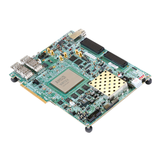
The VCU118 evaluation board for the AMD Virtex UltraScale+ FPGA provides a hardware environment for developing and evaluating designs targeting the UltraScale+ XCVU9P-L2FLGA2104 device. The VCU118 evaluation board provides features common to many evaluation systems, including: • DDR4 and RLD3 component memory •... -
Page 6: Block Diagram
Chapter 1: Introduction Block Diagram A block diagram of the VCU118 evaluation board is shown in Figure 1-1. X-Ref Target - Figure 1-1 X18010-102517 Figure 1‐1: VCU118 Evaluation Board Block Diagram VCU118 Board User Guide Send Feedback UG1224 (v1.5) March 15, 2023... -
Page 7: Board Features
Chapter 1: Introduction Board Features The VCU118 evaluation board features are listed here. Detailed information for each feature is provided in Component Descriptions in Chapter • Virtex UltraScale+ XCVU9P-L2FLGA2104 device ™ • Zynq 7000 SoC XC7Z010 based system controller • Two 2.5 GB DDR4 80-bit component memory interfaces (five [256 Mb x 16] devices each) •... -
Page 8: Board Specifications
Thickness (±5%): 0.061 inch (0.1549 cm) Length: 9.5 inch (24.13 cm) A 3D model of this board is not available. Note: The VCU118 board height exceeds the standard 4.376 inch (11.15 cm) height of a PCI IMPORTANT: ® Express card. -
Page 9: Operating Voltage
Chapter 1: Introduction Operating Voltage +12 V VCU118 Board User Guide Send Feedback UG1224 (v1.5) March 15, 2023... -
Page 10: Chapter 2: Board Setup And Configuration
Figure 2-1 is for visual reference only and might not reflect the current revision of the IMPORTANT: board. The VCU118 board can be damaged by electrostatic discharge (ESD). Follow standard ESD CAUTION! prevention measures when handling the board. Electrostatic Discharge Caution... - Page 11 Chapter 2: Board Setup and Configuration • If you are returning the adapter to AMD Product Support, place it back in its antistatic bag immediately. X-Ref Target - Figure 2-1 Round callout references a component Square callout references a component on the front side of the board...
- Page 12 Chapter 2: Board Setup and Configuration Table 2‐1: VCU118 Board Component Descriptions (Cont’d) Schematic Callout Feature Notes Page Number RLD3 Component Memory, RLD3 72-bit Micron MT44K32M36RB-083F 31-32 component memory I/F C3 (U141-U142) VCU118 Rev. 2.0 board hosts dual clam-shelled Quad SPI Flash...
- Page 13 Chapter 2: Board Setup and Configuration Table 2‐1: VCU118 Board Component Descriptions (Cont’d) Schematic Callout Feature Notes Page Number I2C Bus, Topology, and Switches, I C bus, TI TCA9548APWR C bus MUX (U28) (bottom) I2C Bus, Topology, and Switches, I C bus,...
-
Page 14: Default Switch And Jumper Settings
(J7) PBC36DAAN Notes: 1. VCU118 boards earlier than Rev. 2.0 host a linear BPI 16-bit flash configuration memory, 1 Gb (U133) Micron MT28GU01GAAA1EGC-0SIT at location 6 and on their respective schematic page 54. See Appendix C, BPI Flash Memory for VCU118 Boards Prior to Revision 2.0. -
Page 15: Jumpers
Chapter 2: Board Setup and Configuration Jumpers Figure 2-2 shows the VCU118 board jumper header locations. Each numbered component shown in the figure is keyed to Table 2-3, which identifies the default jumper settings and references the respective schematic page numbers. -
Page 16: Installing The Vcu118 Board In A Pc Chassis
Installation of the VCU118 board inside a computer chassis is required when developing or testing PCI Express® functionality. When the VCU118 board is used inside a computer chassis (that is, plugged in to the PCIe® slot), power is provided from the ATX power supply 4-pin peripheral connector through the... -
Page 17: Fpga Configuration
Figure 2-3. a. Plug the 6-pin 2 x 3 Molex connector on the adapter cable into J15 on the VCU118 board. b. Plug the 4-pin 1 x 4 peripheral power connector from the ATX power supply into the 4-pin adapter cable connector. - Page 18 DIP switch SW16 JTAG switch positions. X-Ref Target - Figure 2-4 ON Position = 1 OFF Position = 0 Figure 2‐4: SW16 JTAG Mode Settings See the VCU118 Software Install and Board Setup Tutorial (XTP449) [Ref 15] for more information. System Controller, page 111 for an overview of query and control of select programmable board features such as clocks, FMC functionality, and power systems.
-
Page 19: Chapter 3: Board Component Descriptions
CCINT • = 0.72V xcvu9p-flga2104-2LV-e CCINT The V value on your board can be found using the VCU118 System Controller Tutorial CCINT (XTP447) [Ref 14] or via the FPGA internal SYSMON function: after Vivado has discovered the XCVU9P in the JTAG chain, the SYSMON module is displayed on the upper left pane. - Page 20 Chapter 3: Board Component Descriptions Encryption Key Battery Backup Circuit The XCVU9P device U1 implements bitstream encryption key technology. The VCU118 board provides the encryption key backup battery circuit shown in Figure 3-1. The Seiko TS518FE rechargeable 1.5V lithium button-type battery B1 is soldered to the board with the positive output connected to the XCVU9P device U1 VBATT pin AT11.
- Page 21 Chapter 3: Board Component Descriptions I/O Voltage Rails There are 16 I/O banks available on the XCVU9P device and the VCU118 board. The voltages applied to the FPGA I/O banks used by the VCU118 board are listed in Table 3-1. Table 3‐1: I/O Bank Voltage Rails...
-
Page 22: Ddr4 Component Memory
° DDR4-2400 ° The VCU118 XCVU9P DDR interface performance is documented in the Virtex UltraScale+ FPGAs Data Sheet: DC and AC Switching Characteristics (DS923) [Ref This dual memory system is connected in 80-bit wide interfaces to the U1 XCVU9P HP banks 71, 72, 73 (C1) and 40, 41, 42 (C2). - Page 23 POD12_DCI DQU6 DDR4_C1_DQ31 POD12_DCI DQU7 DDR4_C1_DQS2_T DIFF_POD12_DCI DQSL_T DDR4_C1_DQS2_C DIFF_POD12_DCI DQSL_C DDR4_C1_DQS3_T DIFF_POD12_DCI DQSU_T DDR4_C1_DQS3_C DIFF_POD12_DCI DQSU_C DDR4_C1_DM2 POD12_DCI DML_B/DBIL_B DDR4_C1_DM3 POD12_DCI DMU_B/DBIU_B DDR4_C1_DQ32 POD12_DCI DQL0 DDR4_C1_DQ33 POD12_DCI DQL1 VCU118 Board User Guide Send Feedback UG1224 (v1.5) March 15, 2023...
- Page 24 POD12_DCI DQL4 DDR4_C1_DQ53 POD12_DCI DQL5 DDR4_C1_DQ54 POD12_DCI DQL6 DDR4_C1_DQ55 POD12_DCI DQL7 DDR4_C1_DQ56 POD12_DCI DQU0 DDR4_C1_DQ57 POD12_DCI DQU1 DDR4_C1_DQ58 POD12_DCI DQU2 DDR4_C1_DQ59 POD12_DCI DQU3 DDR4_C1_DQ60 POD12_DCI DQU4 DDR4_C1_DQ61 POD12_DCI DQU5 VCU118 Board User Guide Send Feedback UG1224 (v1.5) March 15, 2023...
- Page 25 DIFF_POD12_DCI DQSL_T DDR4_C1_DQS8_C DIFF_POD12_DCI DQSL_C DDR4_C1_DQS9_T DIFF_POD12_DCI DQSU_T DDR4_C1_DQS9_C DIFF_POD12_DCI DQSU_C DDR4_C1_DM8 POD12_DCI DML_B/DBIL_B DDR4_C1_DM9 POD12_DCI DMU_B/DBIU_B DDR4_C1_A0 SSTL12_DCI U60-U64 DDR4_C1_A1 SSTL12_DCI U60-U64 DDR4_C1_A2 SSTL12_DCI U60-U64 DDR4_C1_A3 SSTL12_DCI U60-U64 VCU118 Board User Guide Send Feedback UG1224 (v1.5) March 15, 2023...
- Page 26 LVCMOS12 RESET_B U60-U64 DDR4_C1_TEN SSTL12_DCI U60-U64 The connections between the C2 80-bit interface DDR4 component memories (U135-U139) and XCVU9P banks 40, 41, and 42 are listed in Table 3-3. VCU118 Board User Guide Send Feedback UG1224 (v1.5) March 15, 2023...
- Page 27 DDR4_C2_DQ21 POD12_DCI DQL5 U136 AU31 DDR4_C2_DQ22 POD12_DCI DQL6 U136 AV31 DDR4_C2_DQ23 POD12_DCI DQL7 U136 AR33 DDR4_C2_DQ24 POD12_DCI DQU0 U136 AT34 DDR4_C2_DQ25 POD12_DCI DQU1 U136 AT29 DDR4_C2_DQ26 POD12_DCI DQU2 U136 VCU118 Board User Guide Send Feedback UG1224 (v1.5) March 15, 2023...
- Page 28 DDR4_C2_DQS4_C DIFF_POD12_DCI DQSL_C U137 BE39 DDR4_C2_DQS5_T DIFF_POD12_DCI DQSU_T U137 BF39 DDR4_C2_DQS5_C DIFF_POD12_DCI DQSU_C U137 BC34 DDR4_C2_DM4 POD12_DCI DML_B/DBIL_B U137 BE40 DDR4_C2_DM5 POD12_DCI DMU_B/DBIU_B U137 BB36 DDR4_C2_DQ48 POD12_DCI DQL0 U138 VCU118 Board User Guide Send Feedback UG1224 (v1.5) March 15, 2023...
- Page 29 DDR4_C2_DQ71 POD12_DCI DQL7 U139 BC25 DDR4_C2_DQ72 POD12_DCI DQU0 U139 BC26 DDR4_C2_DQ73 POD12_DCI DQU1 U139 BB28 DDR4_C2_DQ74 POD12_DCI DQU2 U139 BC28 DDR4_C2_DQ75 POD12_DCI DQU3 U139 AY27 DDR4_C2_DQ76 POD12_DCI DQU4 U139 VCU118 Board User Guide Send Feedback UG1224 (v1.5) March 15, 2023...
- Page 30 AV26 DDR4_C2_A16_RAS_B SSTL12_DCI RAS_B/A16 U135-U139 AT26 DDR4_C2_CK_T DIFF_SSTL12_DCI CK_T U135-U139 AT27 DDR4_C2_CK_C DIFF_SSTL12_DCI CK_C U135-U139 AW28 DDR4_C2_CKE SSTL12_DCI U135-U139 AN25 DDR4_C2_ACT_B SSTL12_DCI ACT_B U135-U139 BF29 DDR4_C2_PAR SSTL12_DCI ALERT_B U135-U139 VCU118 Board User Guide Send Feedback UG1224 (v1.5) March 15, 2023...
-
Page 31: Rld3 Component Memory
U135-U139 AY35 DDR4_C2_TEN SSTL12_DCI U135-U139 The VCU118 dual DDR4 80-bit memory component interfaces adhere to the constraints guidelines documented in the “DDR3/DDR4 Design Guidelines” section of the UltraScale Architecture-Based FPGAs Memory IP LogiCORE IP Product Guide (PG150) [Ref 4]. The VCU118 board DDR4 memory component interface is a 40... - Page 32 U141 RLD3_C3_72B_DQ26 SSTL12 DQ26 U141 RLD3_C3_72B_DQ27 SSTL12 DQ27 U141 RLD3_C3_72B_DQ28 SSTL12 DQ28 U141 RLD3_C3_72B_DQ29 SSTL12 DQ29 U141 RLD3_C3_72B_DQ30 SSTL12 DQ30 U141 RLD3_C3_72B_DQ31 SSTL12 DQ31 U141 RLD3_C3_72B_DQ32 SSTL12 DQ32 U141 VCU118 Board User Guide Send Feedback UG1224 (v1.5) March 15, 2023...
- Page 33 U142 RLD3_C3_72B_DQ48 SSTL12 DQ12 U142 RLD3_C3_72B_DQ49 SSTL12 DQ13 U142 RLD3_C3_72B_DQ50 SSTL12 DQ14 U142 RLD3_C3_72B_DQ51 SSTL12 DQ15 U142 RLD3_C3_72B_DQ52 SSTL12 DQ16 U142 RLD3_C3_72B_DQ53 SSTL12 DQ17 U142 RLD3_C3_72B_DQ54 SSTL12 DQ18 U142 VCU118 Board User Guide Send Feedback UG1224 (v1.5) March 15, 2023...
- Page 34 DIFF_SSTL12 U142 RLD3_C3_72B_QK7_N DIFF_SSTL12 QK3_B U142 RLD3_C3_72B_QVLD2 DIFF_SSTL12 QVLD0 U142 RLD3_C3_72B_QVLD3 DIFF_SSTL12 QVLD1 U142 RLD3_C3_72B_A0 SSTL12 U141-U142 RLD3_C3_72B_A1 SSTL12 U141-U142 RLD3_C3_72B_A2 SSTL12 U141-U142 RLD3_C3_72B_A3 SSTL12 U141-U142 RLD3_C3_72B_A4 SSTL12 U141-U142 VCU118 Board User Guide Send Feedback UG1224 (v1.5) March 15, 2023...
- Page 35 U141-U142 RLD3_C3_72B_DK0_P DIFF_SSTL12 U141 RLD3_C3_72B_DK0_N DIFF_SSTL12 DK0_B U141 RLD3_C3_72B_DK1_P DIFF_SSTL12 U141 RLD3_C3_72B_DK1_N DIFF_SSTL12 DK1_B U141 RLD3_C3_72B_DK2_P DIFF_SSTL12 U142 RLD3_C3_72B_DK2_N DIFF_SSTL12 DK0_B U142 RLD3_C3_72B_DK3_P DIFF_SSTL12 U142 RLD3_C3_72B_DK3_N DIFF_SSTL12 DK1_B U142 VCU118 Board User Guide Send Feedback UG1224 (v1.5) March 15, 2023...
-
Page 36: Quad Spi Flash Memory
MT44K32M36RB-083E Data Sheet [Ref 18]. Quad SPI Flash Memory VCU118 boards earlier than Rev. 2.0 host a linear BPI 16-bit flash configuration memory, 1 Gb (U133) Micron MT28GU01GAAA1EGC-0SIT. See Appendix C, BPI Flash Memory for VCU118 Boards Prior to Revision 2.0. - Page 37 Chapter 3: Board Component Descriptions X-Ref Target - Figure 3-2 X19992-102617 Figure 3‐2: Dual Quad SPI (2 Gbit) Flash Memory VCU118 Board User Guide Send Feedback UG1224 (v1.5) March 15, 2023...
-
Page 38: System Controller Micro-Sd Card Interface
[Figure 2-1, callout 7] The VCU118 board includes a secure digital input/output (SDIO) interface allowing the U111 XC7Z010 Zynq 7000 SoC system controller access to general purpose nonvolatile micro-SD memory cards and peripherals. The micro-SD card slot is designed to support 50 MHz high speed micro-SD cards. -
Page 39: Digilent Usb Jtag Module
(host side) to micro-B (VCU118 board side J106) USB cable. A 2 mm JTAG header (J3) is also provided in parallel for access by AMD download cables, such as the Platform Cable USB II. JTAG initiated configuration takes priority over the configuration method selected through the FPGA mode pins M[2:0], wired to SW16 positions [2:4]. -
Page 40: Fmc Connector Jtag Bypass
Chapter 3: Board Component Descriptions FMC Connector JTAG Bypass When an FMC is attached to the VCU118 board, it is automatically added to the JTAG chain through electronically controlled single-pole single-throw (SPST) switches U26 (HSPC) and U132 (HPC1). The SPST switches are in a normally closed state and transition to an open state when the FMC is attached. - Page 41 Fixed 250 MHz U14/U21 MHz. U14 output drives U21 dual clock buffer. (250MHZ_CLK1_P/N and 250MHZ_CLK2_P/N) Table 3-7 lists the VCU118 clock sources to FPGA U1 connections. Table 3‐7: VCU118 Clock Sources to XCVU9P FPGA U1 Connections Clock Source Schematic Net Name I/O Standard FPGA (U1) Pin Device/U#.Pin#...
-
Page 42: System Clock
Chapter 3: Board Component Descriptions Table 3‐7: VCU118 Clock Sources to XCVU9P FPGA U1 Connections (Cont’d) Clock Source Schematic Net Name I/O Standard FPGA (U1) Pin Device/U#.Pin# SMA/J35.1 USER_SMA_CLOCK_N LVDS SMA/U38.4 QSFP_SI570_CLOCK_P SMA/U38.5 QSFP_SI570_CLOCK_N ICS85411A/U21.1 250MHZ_CLK1_P LVDS ICS85411A/U21.2 250MHZ_CLK1_N LVDS ICS85411A/U21.3 250MHZ_CLK2_P... - Page 43 Figure 3-4. X-Ref Target - Figure 3-4 X18004-102616 Figure 3‐4: VCU118 System Clock The VCU118 SYSCLKn_300 clocks have an optional clock oscillator source U18 as shown in ² Figure 3-4. SI570 I C programmable low-jitter 3.3V LVDS differential oscillator U18 is connected to the CLK1 P/N inputs (pins 3 (P) and 4 (N)) of clock MUX/quad buffer SI53340 U157.
-
Page 44: Programmable User Clock 1
On power-up, the U18 SI570 user clock defaults to an output frequency of 156.250 MHz. The system controller and user applications can change the output frequency within the range of 10 MHz to 810 MHz. Power cycling the VCU118 evaluation board resets the user clock to the default frequency of 156.250 MHz. - Page 45 The system controller and user applications can change the output frequency within the range of 10 MHz to 810 MHz through an I C interface. Power cycling the VCU118 evaluation board resets the user clock to the default frequency of 156.250 MHz.
-
Page 46: Programmable User Clock 2 (Qsfp Clock)
The Zynq 7000 SoC system controller or FPGA user IP can change the output frequency within the range of 10 MHz to 810 MHz through an I²C interface. Power cycling the VCU118 evaluation board resets the user clock to the default frequency of 156.250 MHz. -
Page 47: 250 Mhz Clock
250 MHz Clock [Figure 2-1, callout 14] The VCU118 evaluation board has an Epson SG5032 3.3V LVDS differential fixed 250 MHz oscillator (U14) connected to 1-to-2 ICS85411 clock buffer U21. The 3.3V ICS85411 U21 has two LVDS output clock pairs: •... -
Page 48: User Sma Clock
[Figure 2-1, callout 15] The VCU118 board provides a pair of SMAs for differential user clock input into FPGA U1 HP bank 45. The P-side SMA J34 signal USER_SMA_CLOCK_P is connected to FPGA U1 HP bank 45 GC pin R32, with the N-side SMA J35 signal USER_SMA_CLOCK_N connected to U1 HP bank 45 GC pin P32. -
Page 49: Jitter Attenuated Clock
[Figure 2-1, callout 16] The VCU118 board includes a Silicon Labs Si5328B jitter attenuator U57 on the back side of the board. The FPGA U1 QSFP1/QSFP2 control interface bank 64 can output QSFP RX differential clocks (QSFP1_RECCLK_P, pin AM23 and QSFP1_RECCLK_N, pin AM22, and QSFP2_RECCLK_P, pin AP23 and QSFP2_RECCLK_N, pin AP22) for jitter attenuation. - Page 50 Chapter 3: Board Component Descriptions X-Ref Target - Figure 3-9 X17999-100416 Figure 3‐9: VCU118 Board QSFP Jitter Attenuated Clock The Silicon Labs Si5328 U57 pin 1 reset net SI5328_RST_B must be driven High to enable IMPORTANT: the device. U57 pin 1 net SI5328_RST_B is level-shifted to 1.8V by U3 and is connected to FPGA U1 bank 64 pin BC21.
-
Page 51: Gty Transceivers
The reference clock for a quad can be sourced from the quad above or quad below the GTY quad of interest. Right Side Quads The six GTY quads on the right side of the VCU118 board have connectivity as listed here: Quad 120: •... - Page 52 Four GTY transceivers allocated to FMC+ HSPC DP[4:7] (J22) Quad 127: • MGTREFCLK0 - FMCP_HSPC_GBTCLK4_M2C_C_P/N (J22) • MGTREFCLK1 - FMCP_HSPC_GBT1_4_M2C_C_P/N (U39) • Four GTY transceivers allocated to FMC+ HSPC DP[16:19] (J22) VCU118 Board User Guide Send Feedback UG1224 (v1.5) March 15, 2023...
- Page 53 Chapter 3: Board Component Descriptions Table 3-8 through Table 3-13 list the VCU118 FPGA U1 GTY transceiver bank 120, 122, 123, 125, 126, 127 connections, respectively. Table 3‐8: VCU118 FPGA U1 GTY Transceiver Bank 120 Connections FPGA FPGA (U1) Pin Connected Connected Pin...
- Page 54 Chapter 3: Board Component Descriptions Table 3‐9: VCU118 FPGA U1 GTY Transceiver Bank 121 Connections FPGA FPGA (U1) Pin Connected Connected Pin Connected Schematic Net Name Bank (U1) Pin Name Name Device AT42 MGTYTXP0_121 FMCP_HSPC_DP0_C2M_P DP0_C2M_P AT43 MGTYTXN0_121 FMCP_HSPC_DP0_C2M_N DP0_C2M_N AR45 MGTYRXP0_121...
- Page 55 Chapter 3: Board Component Descriptions Table 3‐10: VCU118 FPGA U1 GTY Transceiver Bank 122 Connections FPGA FPGA (U1) Pin Connected Connected Pin Connected (U1) Schematic Net Name Bank Name Name Device AK42 MGTYTXP0_122 FMCP_HSPC_DP8_C2M_P DP8_C2M_P AK43 MGTYTXN0_122 FMCP_HSPC_DP8_C2M_N DP8_C2M_N AG45 MGTYRXP0_122 FMCP_HSPC_DP8_M2C_P...
- Page 56 Chapter 3: Board Component Descriptions Table 3‐11: VCU118 FPGA U1 GTY Transceiver Bank 125 Connections FPGA FPGA (U1) Pin Connected Connected Pin Connected (U1) Schematic Net Name Bank Name Name Device AC40 MGTYTXP0_125 FMCP_HSPC_DP12_C2M_P DP12_C2M_P AC41 MGTYTXN0_125 FMCP_HSPC_DP12_C2M_N DP12_C2M_N AC45 MGTYRXP0_125 FMCP_HSPC_DP12_M2C_P...
- Page 57 Chapter 3: Board Component Descriptions Table 3‐12: VCU118 FPGA U1 GTY Transceiver Bank 126 Connections FPGA FPGA (U1) Pin Connected Connected Pin (U1) Schematic Net Name Connected Device Bank Name Name MGTYTXP0_126 FMCP_HSPC_DP4_C2M_P DP4_C2M_P MGTYTXN0_126 FMCP_HSPC_DP4_C2M_N DP4_C2M_N MGTYRXP0_126 FMCP_HSPC_DP4_M2C_P DP4_M2C_P MGTYRXN0_126 FMCP_HSPC_DP4_M2C_N...
- Page 58 Chapter 3: Board Component Descriptions Table 3‐13: VCU118 FPGA U1 GTY Transceiver Bank 127 Connections FPGA FPGA (U1) Pin Connected Connected Pin Connected (U1) Schematic Net Name Bank Name Name Device MGTYTXP0_127 FMCP_HSPC_DP16_C2M_P DP16_C2M_P MGTYTXN0_127 FMCP_HSPC_DP16_C2M_N DP16_C2M_N MGTYRXP0_127 FMCP_HSPC_DP16_M2C_P DP16_M2C_P MGTYRXN0_127 FMCP_HSPC_DP16_M2C_N...
- Page 59 Chapter 3: Board Component Descriptions Left Side Quads The seven GTY quads on the left side of the VCU118 board have connectivity as listed here: Quad 224: • MGTREFCLK0 - not connected • MGTREFCLK1 - not connected • Four GTY transceivers allocated to PCIe lanes 15:12 Quad 225: •...
- Page 60 Four GTY transceivers allocated to FIREFLY (J6) Table 3-14 through Table 3-20 list the VCU118 FPGA U1 GTY transceiver bank 224, 225, 226, 227, 231, 232 and 233 connections, respectively. Table 3‐14: VCU118 FPGA U1 GTY Transceiver Bank 224 Connections FPGA...
- Page 61 Chapter 3: Board Component Descriptions Table 3‐15: VCU118 FPGA U1 GTY Transceiver Bank 225 Connections FPGA FPGA (U1) Pin Name Schematic Net Name Connected Connected (U1) Connected Device Bank Pin Name MGTYTXP0_225 PCIE_TX11_P HSIP(11) MGTYTXN0_225 PCIE_TX11_N HSIN(11) MGTYRXP0_225 PCIE_RX11_P HSOP(11) MGTYRXN0_225 PCIE_RX11_N...
- Page 62 Chapter 3: Board Component Descriptions Table 3‐16: VCU118 FPGA U1 GTY Transceiver Bank 226 Connections FPGA Schematic Net Connected Pin Connected (U1) FPGA (U1) Pin Name Connected Pin Bank Name Name Device MGTYTXP0_226 PCIE_TX7_P HSIP(7) MGTYTXN0_226 PCIE_TX7_N HSIN(7) MGTYRXP0_226 PCIE_RX7_P HSOP(7) MGTYRXN0_226...
- Page 63 Chapter 3: Board Component Descriptions Table 3‐17: VCU118 FPGA U1 GTY Transceiver Bank 227 Connections FPGA FPGA (U1) Pin Name Schematic Net Connected Pin Connected (U1) Connected Pin Bank Name Name Device MGTYTXP0_227 PCIE_TX3_P HSIN(3) MGTYTXN0_227 PCIE_TX3_N HSIP(3) MGTYRXP0_227 PCIE_RX3_P HSIN(3) MGTYRXN0_227...
- Page 64 Chapter 3: Board Component Descriptions Table 3‐18: VCU118 FPGA U1 GTY Transceiver Bank 231 Connections FPGA FPGA (U1) Pin Name Schematic Net Name Connected Connected Pin Connected (U1) Bank Name Device MGTYTXP0_231 QSFP1_TX1_P TX1P MGTYTXN0_231 QSFP1_TX1_N TX1N MGTYRXP0_231 QSFP1_RX1_P RX1P MGTYRXN0_231 QSFP1_RX1_N...
- Page 65 Chapter 3: Board Component Descriptions Table 3‐19: VCU118 FPGA U1 GTY Transceiver Bank 232 Connections FPGA Connected Connected Pin Connected (U1) FPGA (U1) Pin Name Schematic Net Name Bank Name Device MGTYTXP0_232 QSFP2_TX1_P TX1P MGTYTXN0_232 QSFP2_TX1_N TX1N MGTYRXP0_232 QSFP2_RX1_P RX1P MGTYRXN0_232 QSFP2_RX1_N...
- Page 66 Chapter 3: Board Component Descriptions Table 3‐20: VCU118 FPGA U1 GTY Transceiver Bank 233 Connections FPGA Connected Connected Pin Connected (U1) Pin FPGA (U1) Pin Name Schematic Net Name Bank Name Device MGTYTXP0_233 FIREFLY_TX1_P TX1P MGTYTXN0_233 FIREFLY_TX1_N TX1N MGTYRXP0_233 FIREFLY_RX1_P RX1P MGTYRXN0_233...
-
Page 67: Pci Express Endpoint Connectivity
The PCIe transmit and receive signal data paths have a characteristic impedance of 85Ω ±10%. The PCIe clock is routed as a 100Ω differential pair. The XCVU9P-L2FLGA2104 (-2 speed grade) is deployed on the VCU118 to support up to Gen3 x8 on VCU118 pre-Rev. 2.0 boards where V = 0.72V. - Page 68 Chapter 3: Board Component Descriptions X-Ref Target - Figure 3-10 PCI Express Eight-Lane Edge Connector 0.22 μf PCIE_CLK_Q0_C_P PCIE_CLK_Q0_P REFCLK+ PCIE_CLK_Q0_C_N PCIE_CLK_Q0_N REFCLK- 0.22 μf X18024-100616 Figure 3‐10: PCIe Edge Connector Clock VCU118 Board User Guide Send Feedback UG1224 (v1.5) March 15, 2023...
- Page 69 Figure 3-12. The default lane size selection is 16-lane (J7 pins 7 and 8 jumpered). X-Ref Target - Figure 3-12 X17997-100416 Figure 3‐12: PCI Express Lane Size Select Jumper J7 VCU118 Board User Guide Send Feedback UG1224 (v1.5) March 15, 2023...
- Page 70 Chapter 3: Board Component Descriptions Table 3-21 lists the PCIe U2 edge connector wiring to FPGA U1. Table 3‐21: VCU118 Board FPGA U1 to PCIe Edge U2 Connections PCIe Edge U2 FPGA (U1) Pin Schematic Net FPGA (U1) Pin Name Name Pin Num...
- Page 71 Chapter 3: Board Component Descriptions Table 3‐21: VCU118 Board FPGA U1 to PCIe Edge U2 Connections (Cont’d) PCIe Edge U2 FPGA (U1) Pin Schematic Net FPGA (U1) Pin Name Name Pin Num Pin Name MGTYRXP3_227 PCIE_RX0_P HSIN(0) MGTYRXN3_227 PCIE_RX0_N HSIP(0) MGTYRXP2_227 PCIE_RX1_P...
-
Page 72: 28 Gb/S Qsfp+ Module Connectors
[Figure 2-1, callout 18] The VCU118 board contains two quad (4-channel) small form-factor pluggable (28 Gb/s QSFP+) connectors, QSFP1 U145 and QSFP2 U123, which accept 28 Gb/s QSFP+ optical modules. Each connector is housed within a single 28 Gb/s QSFP+ cage assembly. - Page 73 Chapter 3: Board Component Descriptions The connections between the 28 Gb/s QSFP+ module connector U145 and the FPGA are listed in Table 3-22. Table 3‐22: VCU118 Board FPGA U1 to QSFP+ Module QSFP1 U145 Connections QSFP1 U145 FPGA Schematic Net FPGA (U1)
- Page 74 Chapter 3: Board Component Descriptions Table 3‐23: VCU118 Board FPGA U1 to QSFP+ Module QSFP2 U123 Connections QSFP2 U123 FPGA FPGA (U1) FPGA (U1) Pin Name Schematic Net Name (U1) Pin Direction Pin Num Pin Name MGTYTXP0_232 QSFP2_TX1_P Output TX1P MGTYTXN0_232 QSFP2_TX1_N...
-
Page 75: Firefly Connector
[Figure 2-1, callout 41] The VCU118 board contains a 4x28 Gb/s FireFly composite connector pair J6. The FireFly connector system is a two part connector designed for applications up to 28 Gb/s. It is based on two connectors, a micro high-speed edge connector (UEC5 Series, shown rear left) with two rows of 19 positions providing 12 differential lanes and a 10-position positive latch control signal and power connector (UCC8 Series, shown front right). - Page 76 Chapter 3: Board Component Descriptions Figure 3-15 shows the schematic representation. X-Ref Target - Figure 3-15 X17995-100416 Figure 3‐15: FireFly Connector Schematic VCU118 Board User Guide Send Feedback UG1224 (v1.5) March 15, 2023...
- Page 77 Chapter 3: Board Component Descriptions The connections between the J6 and the FPGA are listed in Table 3-24. Table 3‐24: VCU118 Board FPGA U1 to FireFly J6 Connections FireFly J6 FPGA FPGA (U1) FPGA (U1) Pin Name Schematic Net Name (U1) Pin...
-
Page 78: 10/100/1000 Mb/S Tri-Speed Ethernet Phy
[Figure 2-1, callout 19] The VCU118 evaluation board uses the TI PHY device DP83867ISRGZ (U7) for Ethernet communications at 10 Mb/s, 100 Mb/s, or 1000 Mb/s. The board supports SGMII mode only. The PHY connection to a user-provided Ethernet cable is through RJ-45 connector J10, a Wurth 7499111221A with built-in magnetics and status LEDs. -
Page 79: Ethernet Phy Status Leds
Two Ethernet PHY status LEDs are integrated into the metal frame of the J10 RJ-45 connector. These LEDs are visible on the left edge of the VCU118 board when it is installed into a PCIe slot in a PC chassis. The two PHY status LEDs are visible within the frame of the... -
Page 80: Dual Usb-To-Uart Bridge
VCU118 evaluation kit (standard type-A end to host computer, type micro-B end to VCU118 evaluation board connector J4). The CP2105GM is powered by the USB 5V provided by the host PC when the USB cable is plugged into the USB port on the VCU118 evaluation board. -
Page 81: I2C Bus, Topology, And Switches
For more technical information on the CP2105GM and the VCP drivers, see the Silicon Labs website [Ref 22]. AMD UART IP is expected to be implemented in the FPGA logic using IP. See the AXI UART Lite LogiCORE IP Product Guide (PG142) [Ref 10] for more information. - Page 82 0x74 SYSMON IIC X18025-041818 Figure 3‐18: VCU118 IIC Bus The TCA9548 U28 and U80 RESET_B pin 3 is connected to FPGA U1 Bank 64 pin AL25. IMPORTANT: FPGA pin AL25 LVCMOS18 net IIC_MUX_RESET_B must be driven High to enable I²C bus transactions with the devices connected to U28 and U80.
- Page 83 PMBus INA226AIDGS power 0b1000000- U8,U23,U27,U29,U35,U36,U37 0x40-0x48 monitor 0b1001000 SI570_2 clock U38 SI570 0b1011101 0x5D Not used Not used Information about the TCA9548 is available on the TI Semiconductor website [Ref 25]. VCU118 Board User Guide Send Feedback UG1224 (v1.5) March 15, 2023...
-
Page 84: Status And User Leds
Chapter 3: Board Component Descriptions Status and User LEDs [Figure 2-1, callouts 24] Table 3-28 defines VCU118 board status and user LEDs. Table 3‐28: VCU118 Board Status and User LEDs Reference Designator Description ENET PHY link FPGA INIT Combined power good SYS_2V2 ON... -
Page 85: User I/O
EPHY J10 LFT. GREEN ENET link activity User I/O [Figure 2-1, callouts 23, 24, 25, 26] The VCU118 board provides these user and general purpose I/O capabilities: • Eight user LEDs (callout 24) GPIO_LED[7-0]: DS31, DS32, DS33, DS10, DS19, DS8, DS6, DS7 °... -
Page 86: User Gpio Leds
Chapter 3: Board Component Descriptions User GPIO LEDs [Figure 2-1, callouts 24] Figure 3-19 shows the GPIO LED circuit. X-Ref Target - Figure 3-19 X17992-100416 Figure 3‐19: User LEDs VCU118 Board User Guide Send Feedback UG1224 (v1.5) March 15, 2023... -
Page 87: User Pushbuttons
Chapter 3: Board Component Descriptions User Pushbuttons [Figure 2-1, callout 25] Figure 3-20 shows the user pushbuttons circuit. X-Ref Target - Figure 3-20 X17991-100416 Figure 3‐20: User Pushbuttons VCU118 Board User Guide Send Feedback UG1224 (v1.5) March 15, 2023... -
Page 88: Cpu Reset Pushbutton
Figure 3‐21: CPU Reset Pushbutton GPIO DIP Switch [Figure 2-1, callout 26] Figure 3-22 shows the GPIO DIP switch circuit. X-Ref Target - Figure 3-22 X17989-100416 Figure 3‐22: GPIO DIP Switch VCU118 Board User Guide Send Feedback UG1224 (v1.5) March 15, 2023... - Page 89 Chapter 3: Board Component Descriptions Table 3-29 lists the GPIO connections to FPGA U1. Table 3‐29: VCU118 GPIO Connections to FPGA U1 Schematic Net FPGA (U1) FPGA (U1) Pin I/O Standard Device Name Direction GPIO LEDs (Active-High) GPIO_LED signals are wired to FET LED drivers...
-
Page 90: User Pmod Gpio Headers
U41 (PMOD0 J52) and U42 (PMOD1 J53). The level shifters are wired to XCVU9P FPGA U1 banks 47 and 67. The VCU118 complies to PMOD Spec Version 1.2. You must add pull-up to PMOD module for both LVCMOS, LVTTL and I2C. - Page 91 PMOD1_5 J53.4 PMOD1_6_LS LVCMOS12 U42.9 U42.12 PMOD1_6 J53.6 PMOD1_7_LS LVCMOS12 U42.10 U42.11 PMOD1_7 J53.8 For more information about Pmod connector compatible Pmod modules, see the Digilent website [Ref 21]. VCU118 Board User Guide Send Feedback UG1224 (v1.5) March 15, 2023...
-
Page 92: Switches
[Figure 2-1, callout 30] The VCU118 board power switch is SW1. Sliding the switch actuator from the off to on position applies 12VDC power from the 6-pin mini-fit power input connector J15. Green LED DS20 illuminates when power is available at the VCU118 power connector J15, and DS26 illuminates when the VCU118 board power switch is on. - Page 93 The VCU118 evaluation kit provides the adapter cable shown in Figure 3-24 for powering the VCU118 board from the ATX power supply 4-pin peripheral connector. The AMD part number for this cable is 2600304, and is equivalent to the Sourcegate Technologies part number AZCBL-WH-1109-RA4. See [Ref 29] for ordering information.
-
Page 94: Fpga Mezzanine Card Interface
J2 (HPC1). HPC connectors use a 10 x 40 form factor, populated with 400 pins. The connector is keyed so that a mezzanine card, when installed on the VCU118 evaluation board, faces away from the board. - Page 95 The HPC connector at J2 implements a subset of the full FMC HPC connectivity: • 68 single-ended or 34 differential user-defined pairs (34 LA pairs: LA[00:33]) • Two differential clocks • 159 ground and 15 power connections VCU118 Board User Guide Send Feedback UG1224 (v1.5) March 15, 2023...
- Page 96 FMC_HPC1_LA26_N LVDS AL15 VCC12_SW FMC_HPC1_TCK_BUF (2) U19.16 U132.1,U VCC12_SW FMCP_HSPC_TDO_HPC1_TDI (3) 26.2,J22. U132.2,U UTIL_3V3 FMC_HPC1_TDO (3) 13.8 UTIL_3V3 FMC_HPC1_TMS_BUF (2) U19.19 GA1 = 0 = GND UTIL_3V3 UTIL_3V3 UTIL_3V3 VCU118 Board User Guide Send Feedback UG1224 (v1.5) March 15, 2023...
- Page 97 AK14 FMC_HPC1_LA30_P LVDS AK12 FMC_HPC1_LA33_N LVDS AK13 FMC_HPC1_LA30_N LVDS AL12 VADJ_1V8_FPGA FMC_HPC1_LA32_P LVDS AJ13 FMC_HPC1_LA32_N LVDS AJ12 VADJ_1V8_FPGA J2 Sections J/K are no connects (not connected to FPGA U1) VCU118 Board User Guide Send Feedback UG1224 (v1.5) March 15, 2023...
- Page 98 FMCP) specification by providing a subset implementations of the high pin count connectors at J22 (HSPC). FMC+ connectors use a 14 x 40 form factor, populated with 560 pins. The connector is keyed so that a mezzanine card, when installed on the VCU118 evaluation board, faces away from the board.
- Page 99 AM43 FMCP_HSPC_DP8_C2M_P LVDS AK42 FMCP_HSPC_DP3_C2M_P LVDS AL40 FMCP_HSPC_DP8_C2M_N LVDS AK43 FMCP_HSPC_DP3_C2M_N LVDS AL41 FMCP_HSPC_DP7_C2M_P LVDS FMCP_HSPC_DP4_C2M_P LVDS FMCP_HSPC_DP7_C2M_N LVDS FMCP_HSPC_DP4_C2M_N LVDS FMCP_HSPC_DP6_C2M_P LVDS FMCP_HSPC_DP5_C2M_P LVDS FMCP_HSPC_DP6_C2M_N LVDS FMCP_HSPC_DP5_C2M_N LVDS VCU118 Board User Guide Send Feedback UG1224 (v1.5) March 15, 2023...
- Page 100 FMCP_HSPC_IIC_SCL FMCP_HSPC_LA23_N LVDS FMCP_HSPC_IIC_SDA FMCP_HSPC_LA26_P LVDS GA0 = 0 = GND FMCP_HSPC_LA26_N LVDS VCC12_SW FMCP_HSPC_TCK_BUF VCC12_SW FPGA_TDO_FMC_TDI_BUF UTIL_3V3 FMCP_HSPC_TDO_HPC1_TDI UTIL_3V3 FMCP_HSPC_TMS_BUF GA1 = 0 = GND UTIL_3V3 UTIL_3V3 UTIL_3V3 VCU118 Board User Guide Send Feedback UG1224 (v1.5) March 15, 2023...
- Page 101 LVDS FMCP_HSPC_HA13_P LVDS FMCP_HSPC_HA08_N LVDS FMCP_HSPC_HA13_N LVDS FMCP_HSPC_HA12_P LVDS FMCP_HSPC_HA16_P LVDS FMCP_HSPC_HA12_N LVDS FMCP_HSPC_HA16_N LVDS FMCP_HSPC_HA15_P LVDS FMCP_HSPC_HA20_P LVDS FMCP_HSPC_HA15_N LVDS FMCP_HSPC_HA20_N LVDS FMCP_HSPC_HA19_P LVDS FMCP_HSPC_HA19_N LVDS VADJ_1V8_FPGA VADJ_1V8_FPGA VCU118 Board User Guide Send Feedback UG1224 (v1.5) March 15, 2023...
- Page 102 LVDS FMCP_HSPC_LA24_P LVDS FMCP_HSPC_LA29_N LVDS FMCP_HSPC_LA24_N LVDS FMCP_HSPC_LA31_P LVDS FMCP_HSPC_LA28_P LVDS FMCP_HSPC_LA31_N LVDS FMCP_HSPC_LA28_N LVDS FMCP_HSPC_LA33_P LVDS FMCP_HSPC_LA30_P LVDS FMCP_HSPC_LA33_N LVDS FMCP_HSPC_LA30_N LVDS VADJ_1V8_FPGA FMCP_HSPC_LA32_P LVDS FMCP_HSPC_LA32_N LVDS VADJ_1V8_FPGA VCU118 Board User Guide Send Feedback UG1224 (v1.5) March 15, 2023...
- Page 103 LVDS FMCP_HSPC_HA10_P LVDS FMCP_HSPC_HA14_P LVDS FMCP_HSPC_HA10_N LVDS FMCP_HSPC_HA14_N LVDS FMCP_HSPC_HA17_CC_P LVDS FMCP_HSPC_HA18_P LVDS FMCP_HSPC_HA17_CC_N LVDS FMCP_HSPC_HA18_N LVDS FMCP_HSPC_HA21_P LVDS FMCP_HSPC_HA22_P LVDS FMCP_HSPC_HA21_N LVDS FMCP_HSPC_HA22_N LVDS FMCP_HSPC_HA23_P LVDS FMCP_HSPC_HA23_N LVDS VCU118 Board User Guide Send Feedback UG1224 (v1.5) March 15, 2023...
- Page 104 LVDS FMCP_HSPC_REFCLK_M2C_N LVDS AL34 FMCP_HSPC_DP16_C2M_P LVDS FMCP_HSPC_SYNC_M2C_P LVDS AM36 FMCP_HSPC_DP16_C2M_N LVDS FMCP_HSPC_SYNC_M2C_N LVDS AN36 FMCP_HSPC_DP17_C2M_P LVDS FMCP_HSPC_DP17_C2M_N LVDS FMCP_HSPC_DP18_C2M_P LVDS VCC12_SW FMCP_HSPC_DP18_C2M_N LVDS VCC12_SW FMCP_HSPC_DP19_C2M_P LVDS VCC12_SW FMCP_HSPC_DP19_C2M_N LVDS VCU118 Board User Guide Send Feedback UG1224 (v1.5) March 15, 2023...
- Page 105 3. FMCP_HSPC_H_PRSNT_M2C_B is level-shifted by U44 and is connected to FPGA pin U1.AM33. 4. FMCP_HSPC_Z_PRSNT_M2C_B is level-shifted by U44 and is connected to FPGA pin U1.AM29. 5. FMCP_HSPC_GBTCLKn_M2C_P/N are series capacitor coupled, the nets connected to FPGA U1 are FMCP_HSPC_GBTCLKn_M2C_C_P/N. VCU118 Board User Guide Send Feedback UG1224 (v1.5) March 15, 2023...
-
Page 106: Vcu118 Board Power System
Chapter 3: Board Component Descriptions VCU118 Board Power System [Figure 2-1, callout 31] The VCU118 hosts a Maxim PMBus based power system. Figure 3-27 shows the VCU118 power system block diagram. X-Ref Target - Figure 3-27 X17984-100416 Figure 3‐27: VCU118 Power System Block Diagram... - Page 107 Chapter 3: Board Component Descriptions The VCU118 evaluation board uses power regulators and PMBus compliant point of load (POL) controllers from Maxim Integrated Circuits to supply the core and auxiliary voltages listed in Table 3-33. Table 3‐33: Onboard Power System Devices Reference...
-
Page 108: Fmc Vadj_1V8 Power Rail
1.2V, 1.5V, 1.8V, and 0.0V. • When two FMC cards are attached with differing VADJ requirements, VADJ_1V8 is set to the lowest value compatible with the VCU118 board and the FMC modules, within the available choices of 1.2V, 1.5V, 1.8V, and 0.0V. •... - Page 109 Chapter 3: Board Component Descriptions The Maxim PMBus controller and INA226 power monitor I C bus mapping is shown in Table 3-34. Table 3‐34: VCU118 Voltage Regulators and INA226 Power Monitors PMBus Regulators and INA226 Map Schematic PMBus INA226 Rail Regulator Type...
-
Page 110: Cooling Fan
The XCVU9P FPGA U1 cooling fan connector is shown in Figure 3-28. The VCU118 fan circuit uses a Maxim MAX6643 fan controller that autonomously monitors the FPGA die temperature pins DXP and DXN. The fan circuit is set up to increase fan speed as the FPGA temperature increases. -
Page 111: System Controller
[Figure 2-1, callout 36] The VCU118 board includes an onboard Zynq 7000 SoC as the system controller. A host PC resident graphical user interface for the system controller (SCUI) is provided on the VCU118 website. The SCUI can be used to query and control select programmable features such as clocks, FMC functionality, and power systems. -
Page 112: Configuration Options
Controller utility. Configuration Options [Figure 2-1, callout 35] VCU118 boards earlier than Rev. 2.0 host a linear BPI 16-bit flash configuration memory, 1 Gb (U133) Micron MT28GU01GAAA1EGC-0SIT. See Appendix C, BPI Flash Memory for VCU118 Boards Prior to Revision 2.0. - Page 113 Si5335A U122 is wired to the EMCCLK pin of the FPGA on bank 65 pin AL20. This allows the creation of bitstreams to configure the FPGA over the 8-bit datapath from the dual Quad SPI flash memory at a maximum synchronous read rate of 90 MHz. VCU118 Board User Guide Send Feedback UG1224 (v1.5) March 15, 2023...
-
Page 114: Appendix A: Vita 57.1 And 57.4 Fmc Connector Pinouts
Figure A-1 shows the pinout of the FPGA mezzanine card (FMC) high pin count (HPC) J2 defined by the VITA 57.1 FMC specification. For a description of how the VCU118 evaluation board implements the FMC specification, see FPGA Mezzanine Card Interface, page X-Ref Target - Figure A-1 Figure A‐1: FMC Connector Pinouts... - Page 115 Figure A-2 shows the pinout of the FPGA mezzanine card plus (FMCP) connector J22 defined by the VITA 57.4 FMC specification. For a description of how the VCU118 evaluation board implements the FMC specification, see FPGA Mezzanine Card Interface, page X-Ref Target - Figure A-2 Figure A‐2: FMCP Connector Pinouts...
-
Page 116: Appendix B: Xilinx Constraints File
Xilinx Constraints File Overview The Xilinx design constraints (XDC) file template for the VCU118 board provides for designs targeting the VCU118 evaluation board. Net names in the constraints correlate with net names on the latest VCU118 evaluation board schematic. Users must identify the appropriate pins and replace the net names with net names in the user RTL. -
Page 117: Appendix C: Bpi Flash Memory For Vcu118 Boards Prior To Revision
BPI Flash Memory for VCU118 Boards Prior to Revision 2.0 Configuration Options [Figure 2-1, callout 35] The VCU118 board supports two of the seven UltraScale FPGA configuration modes: • Master BPI using the onboard linear BPI flash memory • JTAG using: USB JTAG configuration port (Digilent module U115) °... - Page 118 Appendix C: BPI Flash Memory for VCU118 Boards Prior to Revision 2.0 Figure C-1 shows mode switch SW16. X-Ref Target - Figure C-1 ON Position = 1 OFF Position = 0 X18009-091818 Figure C‐1: SW16 JTAG Mode Setting The mode pins settings on SW16 determine if the linear BPI flash is used for configuring the FPGA.
-
Page 119: Linear Bpi Flash Memory
Appendix C: BPI Flash Memory for VCU118 Boards Prior to Revision 2.0 Linear BPI Flash Memory [Figure 2-1, callout 6] The linear BPI flash memory located at U133 provides 128 MB (1 Gbit) of nonvolatile storage that can be used for configuration or software storage. The data, address, and control signals are connected to the U1 XCVU9P bank 65. - Page 120 Appendix C: BPI Flash Memory for VCU118 Boards Prior to Revision 2.0 Add these constraints for compression to designs targeted for the VCU118 board. • When loading from the BPI flash memory: set_property BITSTREAM.CONFIG.EXTMASTERCCLK_EN div-1 [current_design] set_property BITSTREAM.CONFIG.BPI_SYNC_MODE Type1 [current_design] set_property CONFIG_MODE BPI16 [current_design] *set_property BITSTREAM.GENERAL.COMPRESS TRUE [current_design]...
- Page 121 Appendix C: BPI Flash Memory for VCU118 Boards Prior to Revision 2.0 The connections between the BPI flash memory and the FPGA are listed in Table C-2. Table C‐2: BPI Flash Memory Connections to FPGA U1 U58 BPI Flash Memory FPGA (U1) Pin...
- Page 122 Appendix C: BPI Flash Memory for VCU118 Boards Prior to Revision 2.0 Table C‐2: BPI Flash Memory Connections to FPGA U1 (Cont’d) U58 BPI Flash Memory FPGA (U1) Pin Net Name I/O Standard Pin # Pin Name BB18 BPI_FLASH_A16 LVCMOS18 BC18 BPI_FLASH_A17...
-
Page 123: Bpi Flash Memory Constraints
Appendix C: BPI Flash Memory for VCU118 Boards Prior to Revision 2.0 BPI Flash Memory Constraints # BPI FLASH # BPI_FLASH_D[3:0] are wired to FPGA U1 Bank 0 # CONFIGURATION BITS D[3:0} ARE NOT USER ACCESSIBLE # PACKAGE_PIN AP11 - BPI_FLASH_D0 Bank 0 - D00_MOSI_0... - Page 124 Appendix C: BPI Flash Memory for VCU118 Boards Prior to Revision 2.0 set_property IOSTANDARD LVCMOS18 [get_ports "BPI_FLASH_A1"]; set_property PACKAGE_PIN AV20 [get_ports "BPI_FLASH_A2"]; set_property IOSTANDARD LVCMOS18 [get_ports "BPI_FLASH_A2"]; set_property PACKAGE_PIN AW20 [get_ports "BPI_FLASH_A3"]; set_property IOSTANDARD LVCMOS18 [get_ports "BPI_FLASH_A3"]; set_property PACKAGE_PIN AU19 [get_ports "BPI_FLASH_A4"];...
- Page 125 Appendix C: BPI Flash Memory for VCU118 Boards Prior to Revision 2.0 set_property IOSTANDARD LVCMOS18 [get_ports "BPI_FLASH_A20"]; set_property PACKAGE_PIN BD17 [get_ports "BPI_FLASH_A21"]; set_property IOSTANDARD LVCMOS18 [get_ports "BPI_FLASH_A21"]; set_property PACKAGE_PIN BC20 [get_ports "BPI_FLASH_A22"]; set_property IOSTANDARD LVCMOS18 [get_ports "BPI_FLASH_A22"]; set_property PACKAGE_PIN BD20 [get_ports "BPI_FLASH_A23"];...
-
Page 126: Appendix D: Regulatory And Compliance Information
Regulatory and Compliance Information Overview This product is designed and tested to conform to the European Union directives and standards described in this section. VCU118 Evaluation Kit — Master Answer Record (AR 68268) For Technical Support, open a Support Service Request. -
Page 127: Safety
This product complies with Directive 2002/95/EC on the restriction of hazardous substances (RoHS) in electrical and electronic equipment. This product complies with CE Directives 2006/95/EC, Low Voltage Directive (LVD) and 2004/108/EC, Electromagnetic Compatibility (EMC) Directive. VCU118 Board User Guide Send Feedback UG1224 (v1.5) March 15, 2023... -
Page 128: Appendix E: Additional Resources And Legal Notices
Topics include design assistance, advisories, and troubleshooting tips. Finding Additional Documentation The AMD Adaptive Computing Documentation Portal is an online tool that provides robust search and navigation for documentation using your web browser. To access the Documentation Portal, go to https://docs.xilinx.com. -
Page 129: Design Hubs
Note: on the Xilinx website. References The most up to date information related to the VCU118 board and its documentation is available on the following websites. VCU118 Evaluation Kit VCU118 Evaluation Kit – Master Answer Record (AR 68268) These documents provide supplemental material useful with this guide: 1. - Page 130 InTune™ Digital PowerTool Software Version 1.08.02 is available. Users will have to create a Maxim account and login before they can see the link to download the GUI. 29. The AMD ATX cable part number 2600304 is manufactured by Sourcegate Technologies and is equivalent to the Sourcegate Technologies part number AZCBL-WH-11009.
- Page 131 Configuration. Added Quad SPI Flash Memory Finding Additional Documentation. Revised Appendix B, Master Constraints File Listing. Reorganized appendices to include a new Appendix C, BPI Flash Memory for VCU118 Boards Prior to Revision 2.0. 10/15/2016 Initial Xilinx release. VCU118 Board User Guide Send Feedback UG1224 (v1.5) March 15, 2023...
- Page 132 AMD assumes no obligation to update or otherwise correct or revise this information. However, AMD reserves the right to revise this information and to make changes from time to time to the content hereof without obligation of AMD to notify any person of such revisions or changes.
Need help?
Do you have a question about the VCU118 and is the answer not in the manual?
Questions and answers