Table of Contents
Advertisement
Quick Links
Advertisement
Table of Contents

Related Manuals for Alinx AX7Z100


Summarization of Contents
Part 2: AC7Z100 Core Board Components
Part 2.1: AC7Z100 Core Board Introduction
Overview of the AC7Z100 core board, its ZYNQ chip, and memory.
Part 2.2: ZYNQ Chip Details
Detailed specifications of the Xilinx Zynq7000 series chip, including PS and PL parameters.
Part 2.3: DDR3 DRAM Configuration
Explains the DDR3 DRAM setup, including PS and PL side pin assignments.
Part 2.4: QSPI Flash Specification
Details the QSPI FLASH configuration and its role as a boot device.
Part 2.5: eMMC Flash Interface
Covers the 8GB eMMC FLASH chip, its interface, and system use.
Part 2.6: Clock Configuration
Describes the system clock sources for PS, PL, and GTX transceivers.
Part 2.7: Core Board LED Indicators
Details the core board's LED indicators for power and configuration status.
Part 2.8: Reset Circuit
Explains the reset circuit and its connection to the carrier board's reset button.
Part 2.9: Power Supply Design
Details the power supply architecture and voltage distribution on the core board.
Part 2.10: Core Board Dimensions
Provides the physical size and dimension drawing of the AC7Z100 core board.
Part 2.11: Board-to-Board Connector Pin Assignments
Lists the pin assignments for the four 120-pin inter-board connectors.
Part 3: Carrier Board Interfaces and Features
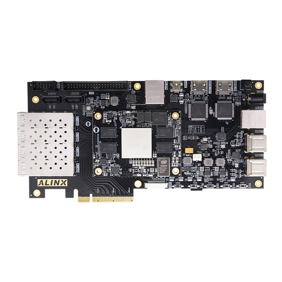
Part 3.1: Carrier Board Introduction
Overview of the carrier board's features and interfaces.
Part 3.2: USB to Serial Port
Details the USB to serial interface for debugging using a CP2102GM chip.
Part 3.3: Gigabit Ethernet Interface
Explains the dual Gigabit Ethernet interfaces connected to PS and PL.
Part 3.4: USB2.0 Host Interface
Describes the four USB 2.0 HOST interfaces utilizing USB3320C and USB2514 chips.
Part 3.5: HDMI Output Interface
Covers the HDMI output interface using the ADV7511 chip.
Part 3.6: HDMI Input Interface
Details the HDMI input interface using SIL9011/SIL9013 chips.
Part 3.7: SFP Interface
Explains the four SFP optical interfaces for high-speed data communication.
Part 3.8: PCIe Slot
Describes the PCIe x8 interface for high-speed data communication.
Part 3.9: SD Card Slot
Covers the Micro SD card slot for system storage and boot files.
Part 3.10: Expansion Header
Details the 40-pin expansion header for connecting external modules.
Part 3-11: Carrier Board LED Lights
Describes the 7 LEDs on the carrier board, including user-controlled LEDs.
Part 3-12: Reset and User Buttons
Details the reset button and four user buttons for system interaction.
Part 3-13: JTAG Debug Port
Explains the JTAG interface for programming and debugging the ZYNQ chip.
Part 3-14: DIP Switch Configuration
Covers the DIP switch for configuring the ZYNQ system's startup mode.
Part 3-15: Carrier Board Power Supply
Details the power supply design and voltage regulation for the carrier board.
Part 3.16: Fan Control
Explains the fan for cooling the ZYNQ chip and its control mechanism.
Part 3.17: Dimensional Structure
Provides the physical dimensions and top view diagram of the carrier board.
Need help?
Do you have a question about the AX7Z100 and is the answer not in the manual?
Questions and answers