
Related Manuals for Altera Cyclone III 3C120


Summary of Contents for Altera Cyclone III 3C120
- Page 1 Cyclone III 3C120 Development Board Reference Manual 101 Innovation Drive Document Version: San Jose, CA 95134 Document Date: March 2009 www.altera.com Arrow.com. Downloaded from...
- Page 2 Altera warrants performance of its semiconductor products to current specifications in accordance with Altera's standard warranty, but reserves the right to make changes to any products and services at any time without notice. Altera assumes no responsibility or liability arising out of the application or use of any information, product, or service described herein except as expressly agreed to in writing by Altera Corporation.
-
Page 3: Table Of Contents
Graphics LCD (J13) ..............2–33 © March 2009 Altera Corporation Cyclone III 3C120 Development Board Reference Manual Arrow.com. Arrow.com. - Page 4 How to Contact Altera ........
-
Page 5: Chapter 1. Overview
® enable the inter-operability of the Cyclone III device, allowing application-specific customization of the development board. For more information about the Altera Video and Image Processing Suite MegaCore functions, refer to the Video and Image Processing Suite User Guide. -
Page 6: Board Component Blocks
■ Quartus II development software’s power optimization tools Board Component Blocks The board features the following major component blocks: ■ 780-pin Altera Cyclone III EP3C120 FPGA in a BGA package 119K logic elements (LEs) ■ 3,888 Kbits of memory ■... - Page 7 Speaker header ■ ■ Displays 128 × 64 graphics LCD ■ 16 × 2 line character LCD ■ © March 2009 Altera Corporation Cyclone III 3C120 Development Board Reference Manual Arrow.com. Arrow.com. Arrow.com. Arrow.com. Arrow.com. Arrow.com. Arrow.com. Downloaded from Downloaded from...
-
Page 8: Block Diagram
256MB DDR2 Audio Amp Dual Channel (x72) Speaker 50 MHz Header Buttons/ Quad 7-Seg/ Switches User LEDs Cyclone III 3C120 Development Board Reference Manual © March 2009 Altera Corporation Arrow.com. Arrow.com. Arrow.com. Arrow.com. Arrow.com. Arrow.com. Arrow.com. Arrow.com. Downloaded from Downloaded from... -
Page 9: Handling The Board
When handling the board, it is important to observe the following precaution: Static Discharge Precaution: Without proper anti-static handling, the board can be damaged. Therefore, use anti-static handling precautions when touching the board. © March 2009 Altera Corporation Cyclone III 3C120 Development Board Reference Manual Arrow.com. Arrow.com. Arrow.com. Arrow.com. - Page 10 1–6 Chapter 1: Overview Handling the Board Cyclone III 3C120 Development Board Reference Manual © March 2009 Altera Corporation Arrow.com. Arrow.com. Arrow.com. Arrow.com. Arrow.com. Arrow.com. Arrow.com. Arrow.com. Arrow.com. Arrow.com. Downloaded from Downloaded from Downloaded from Downloaded from Downloaded from Downloaded from...
-
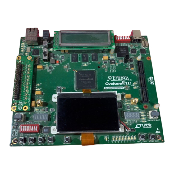
Page 11: Introduction
This section provides an overview of the Cyclone III development board, including an annotated board image and component descriptions. Figure 2–1 shows the top view of the Cyclone III development board. © March 2009 Altera Corporation Cyclone III 3C120 Development Board Reference Manual Arrow.com. Arrow.com. Arrow.com. Arrow.com. Arrow.com. - Page 12 Green LED that illuminates when the FPGA is successfully configured. D12 through D15 Channel activity LEDs Green LEDs that indicate the RX and TX activity on the HSMC Ports A or B. Cyclone III 3C120 Development Board Reference Manual © March 2009 Altera Corporation Arrow.com.
- Page 13 14-pin LCD display. Graphics LCD 30-position dot matrix graphics LCD display. Memory Flash 64 MB of flash memory with a 16-bit data bus. © March 2009 Altera Corporation Cyclone III 3C120 Development Board Reference Manual Arrow.com. Arrow.com. Arrow.com. Arrow.com. Arrow.com. Arrow.com. Arrow.com.
-
Page 14: Featured Fpga (U20)
Table 2–3. Cyclone III Component Reference and Manufacturing Information Manufacturing Manufacturer Board Reference Description Manufacturer Part Number Website Memory rich FPGA device Altera Corporation EP3C120F780 www.altera.com Cyclone III 3C120 Development Board Reference Manual © March 2009 Altera Corporation Arrow.com. Arrow.com. Arrow.com. Arrow.com. Arrow.com. Arrow.com. Arrow.com. Arrow.com. Arrow.com. Arrow.com. -
Page 15: I/O And Clocking Resources
2.5-V LVDS (1 single-ended, 2 differential) Device I/O total: 491 For additional information about Altera devices, go to www.altera.com/products/devices. I/O and Clocking Resources This section lists specific I/O and clocking resources available with the EP3C120F780C7 device, which is the largest of the Cyclone III devices. -
Page 16: Max Ii Cpld
65 I/O 73 I/O 71 I/O MAX II CPLD The board utilizes an Altera MAX II CPLD for the following purposes: ■ Power-up configuration of the FPGA from flash memory Embedded USB-Blaster core for USB-based configuration of the FPGA ■... - Page 17 2.5 V Input FACTORY_CONFIGn 1.8 V Output FLASH_ACTIVE 1.8 V Output FLASH_BYTEn 1.8 V Output FLASH_CEn © March 2009 Altera Corporation Cyclone III 3C120 Development Board Reference Manual Arrow.com. Arrow.com. Arrow.com. Arrow.com. Arrow.com. Arrow.com. Arrow.com. Arrow.com. Arrow.com. Arrow.com. Arrow.com. Arrow.com. Arrow.com.
- Page 18 FSA[5] 1.8 V Output FSA[6] 1.8 V Output FSA[7] 1.8 V Output FSA[8] 1.8 V Output FSA[9] Cyclone III 3C120 Development Board Reference Manual © March 2009 Altera Corporation Arrow.com. Arrow.com. Arrow.com. Arrow.com. Arrow.com. Arrow.com. Arrow.com. Arrow.com. Arrow.com. Arrow.com. Arrow.com.
- Page 19 — GNDINT — GNDINT — GNDINT — GNDINT — GNDINT — GNDINT — © March 2009 Altera Corporation Cyclone III 3C120 Development Board Reference Manual Arrow.com. Arrow.com. Arrow.com. Arrow.com. Arrow.com. Arrow.com. Arrow.com. Arrow.com. Arrow.com. Arrow.com. Arrow.com. Arrow.com. Arrow.com. Arrow.com. Arrow.com.
- Page 20 MAX_FACTORY 2.5 V Output MAX_LOAD 1.8 V Input MAX_OEn 1.8 V Input MAX_RESERVE[0] 1.8 V Input MAX_RESERVE[1] Cyclone III 3C120 Development Board Reference Manual © March 2009 Altera Corporation Arrow.com. Arrow.com. Arrow.com. Arrow.com. Arrow.com. Arrow.com. Arrow.com. Arrow.com. Arrow.com. Arrow.com. Arrow.com.
- Page 21 RESERVED_INPUT — — RESERVED_INPUT — — RESERVED_INPUT — — RESERVED_INPUT — — RESERVED_INPUT © March 2009 Altera Corporation Cyclone III 3C120 Development Board Reference Manual Arrow.com. Arrow.com. Arrow.com. Arrow.com. Arrow.com. Arrow.com. Arrow.com. Arrow.com. Arrow.com. Arrow.com. Arrow.com. Arrow.com. Arrow.com. Arrow.com. Arrow.com.
- Page 22 USB_PHY_FD[12] 2.5 V Bidirectional USB_PHY_FD[13] 2.5 V Bidirectional USB_PHY_FD[14] 2.5 V Bidirectional USB_PHY_FD[15] 2.5 V Bidirectional USB_PHY_FD[2] Cyclone III 3C120 Development Board Reference Manual © March 2009 Altera Corporation Arrow.com. Arrow.com. Arrow.com. Arrow.com. Arrow.com. Arrow.com. Arrow.com. Arrow.com. Arrow.com. Arrow.com. Arrow.com.
- Page 23 VCCIO1 — Power VCCIO2 — Power VCCIO2 — Power VCCIO2 — Power VCCIO2 © March 2009 Altera Corporation Cyclone III 3C120 Development Board Reference Manual Arrow.com. Arrow.com. Arrow.com. Arrow.com. Arrow.com. Arrow.com. Arrow.com. Arrow.com. Arrow.com. Arrow.com. Arrow.com. Arrow.com. Arrow.com. Arrow.com. Arrow.com.
-
Page 24: Configuration, Status, And Setup Elements
Note to Table 2–5: (1) For more information about the MAX II pin-out, refer to the Altera website at www.altera.com/literature/lit-dp.jsp. Table 2–6 lists the MAX II component reference and manufacturing information. Table 2–6. MAX II Component Reference and Manufacturing Information... -
Page 25: Configuration
USB cable along with the embedded USB-Blaster. Using an external USB-Blaster with the JTAG header requires disabling the embedded USB-Blaster function. See Table 2–7. © March 2009 Altera Corporation Cyclone III 3C120 Development Board Reference Manual Arrow.com. Arrow.com. Arrow.com. Arrow.com. Arrow.com. -
Page 26: Fpga Programming From Flash Memory
(1) for this feature to be enabled. If the SW1 switch is in the closed (0) position, the PFL megafunction in the MAX II CPLD is disabled. Cyclone III 3C120 Development Board Reference Manual © March 2009 Altera Corporation Arrow.com. -
Page 27: Flash Programming Over Usb Interface
USB 2.0 interface and the Quartus II Programmer ’s JTAG mode. The development kit implements the Altera PFL megafunction for flash programming. The PFL is a block of logic that is programmed into an Altera programmable logic device (FPGA or CPLD). The PFL functions as a utility for writing to a compatible flash device. -
Page 28: Power Display (U28)
This section discusses: JTAG control DIP switch ■ ■ MAX II device control DIP switch System reset and configuration push buttons ■ Cyclone III 3C120 Development Board Reference Manual © March 2009 Altera Corporation Arrow.com. Arrow.com. Arrow.com. Arrow.com. Arrow.com. -
Page 29: Jtag Control Dip Switch
Table 2–11. JTAG Control Switch Component Reference and Manufacturing Information Board Manufacturing Reference Description Manufacturer Part Number Four-position slider DIP switch C&K Components ITT industries TDA04H0SB1 © March 2009 Altera Corporation Cyclone III 3C120 Development Board Reference Manual Arrow.com. Arrow.com. Arrow.com. Arrow.com. Arrow.com. Arrow.com. Arrow.com. Arrow.com. Arrow.com. Arrow.com. Arrow.com. -
Page 30: Max Ii Device Control Dip Switch
MAX II device. The FACTORY_CONFIG pin forces a reconfiguration of the FPGA with the factory default FPGA design, which is located at the base of flash memory. See Table 2–14. Cyclone III 3C120 Development Board Reference Manual © March 2009 Altera Corporation Arrow.com. Arrow.com. Arrow.com. -
Page 31: Power Select Rotary Switch
2.5V (Ethernet, LEDs, LCD) — All 3.3-V power (voltage only) 3.3V — All 5.0-V power (voltage only) 5.0V © March 2009 Altera Corporation Cyclone III 3C120 Development Board Reference Manual Arrow.com. Arrow.com. Arrow.com. Arrow.com. Arrow.com. Arrow.com. Arrow.com. Arrow.com. Arrow.com. Arrow.com. -
Page 32: Pgm Config Select Rotary Switch
Table 2–19. Power Select Rotary Switch Component Reference and Manufacturing Information Manufacturing Manufacturer Board Reference Description Manufacturer Part Number Website Speaker header Samtec TSW-104-07-G-S www.samtec.com Cyclone III 3C120 Development Board Reference Manual © March 2009 Altera Corporation Arrow.com. Arrow.com. Arrow.com. Arrow.com. Arrow.com. Arrow.com. Arrow.com. Arrow.com. Arrow.com. Arrow.com. -
Page 33: Clocking Circuitry
CLK7 Bank 3 Bank 4 1.8 V 1.8 V 3.3V 1.8V HSMA_CLK_IN0 HSMA_CONN_CLK_IN0 SMA Input 50 MHz © March 2009 Altera Corporation Cyclone III 3C120 Development Board Reference Manual Arrow.com. Arrow.com. Arrow.com. Arrow.com. Arrow.com. Arrow.com. Arrow.com. Arrow.com. Arrow.com. Arrow.com. Arrow.com. -
Page 34: Cyclone Iii Fpga Clock Outputs
1.8 V 1.8 V ENET_GTX_CLK ENET PLL4 DDR2 DDR2 SRAM SMA Output Table 2–20 shows the clocking parts list. Cyclone III 3C120 Development Board Reference Manual © March 2009 Altera Corporation Arrow.com. Arrow.com. Arrow.com. Arrow.com. Arrow.com. Arrow.com. Arrow.com. Arrow.com. Arrow.com. -
Page 35: Oscillators
Crystal oscillator for Ethernet PHY 50.000 MHz Crystal oscillator for Cyclone III FPGA PLL 125.000 MHz Crystal oscillator for Cyclone III FPGA PLL © March 2009 Altera Corporation Cyclone III 3C120 Development Board Reference Manual Arrow.com. Arrow.com. Arrow.com. Arrow.com. Arrow.com. Arrow.com. -
Page 36: General User Interfaces
Manufacturing Manufacturer Board Reference Description Manufacturer Part Number Website S1 through S5 Push button switch Panasonic EVQPAC07K www.panasonic.com Cyclone III 3C120 Development Board Reference Manual © March 2009 Altera Corporation Arrow.com. Arrow.com. Arrow.com. Arrow.com. Arrow.com. Arrow.com. Arrow.com. Arrow.com. Arrow.com. Arrow.com. -
Page 37: User-Defined Dip Switches
Cyclone III device. There is no board-specific function for these LEDs. Table 2–27 lists the general user LED reference number, schematic signal name, and corresponding Cyclone III device pin number. © March 2009 Altera Corporation Cyclone III 3C120 Development Board Reference Manual Arrow.com. Arrow.com. Arrow.com. Arrow.com. Arrow.com. -
Page 38: Hsmc User-Defined Leds
User-defined but labeled RX in silk-screen for 1.8 V HSMB_RX_LED HSMC Port B. Table 2–30 lists the HSMC user-defined LED component reference and manufacturing information. Cyclone III 3C120 Development Board Reference Manual © March 2009 Altera Corporation Arrow.com. Arrow.com. Arrow.com. Arrow.com. Arrow.com. -
Page 39: Ddr2 User-Defined Leds
Part Number Website D11 and D16 Green LED, 1206, Lumex, Inc. SML-LX1206GC-TR www.lumex.com SMT, clear lens 2.1 V © March 2009 Altera Corporation Cyclone III 3C120 Development Board Reference Manual Arrow.com. Arrow.com. Arrow.com. Arrow.com. Arrow.com. Arrow.com. Arrow.com. Arrow.com. Arrow.com. Arrow.com. -
Page 40: 7-Segment Displays
SEVEN_SEG_SEL3 U30 pin 4 User-defined display select signal 1.8 V SEVEN_SEG_SEL4 U30 pin 6 User-defined display select signal 1.8 V SEVEN_SEG_MINUS Cyclone III 3C120 Development Board Reference Manual © March 2009 Altera Corporation Arrow.com. Arrow.com. Arrow.com. Arrow.com. Arrow.com. Arrow.com. Arrow.com. -
Page 41: Power 7-Segment Display
LCD. These two share a common bus but have separate control signals so they can operate simultaneously. This section describes both displays. © March 2009 Altera Corporation Cyclone III 3C120 Development Board Reference Manual Arrow.com. Arrow.com. Arrow.com. Arrow.com. -
Page 42: Character Lcd (J4)
Lumex LCD display device. The 8-bit data bus is shared with the graphics LCD, but the control signals are all separate. Cyclone III 3C120 Development Board Reference Manual © March 2009 Altera Corporation Arrow.com. -
Page 43: Graphics Lcd (J13)
For the graphics LCD data sheet and related documentation, visit www.optrex.com. Table 2–39 lists the graphics LCD pin name, description, and type. Signal name and direction are relative to the Cyclone III FPGA. © March 2009 Altera Corporation Cyclone III 3C120 Development Board Reference Manual Arrow.com. Arrow.com. Arrow.com. Arrow.com. Arrow.com. - Page 44 (1) For the corresponding Cyclone III device pin number, refer to the MAX II device pin-out information in Table 2–5 on page 2–7. For more information about the data sheet and related documentation, visit Lumex at www.lumex.com Cyclone III 3C120 Development Board Reference Manual © March 2009 Altera Corporation Arrow.com. Arrow.com. Arrow.com.
- Page 45 Board defaults graphics LCD interface to 80 series CPU mode and parallel interface. These defaults can be modified by writing to the appropriate register in the MAX II CPLD using the FSM bus. © March 2009 Altera Corporation Cyclone III 3C120 Development Board Reference Manual Arrow.com. Arrow.com. Arrow.com. Arrow.com.
- Page 46 Status Status Busy Flag Bus Holder Decoder Internal Bus Line Reset MPU Interface D5 to D0 (SI) (SCL) Cyclone III 3C120 Development Board Reference Manual © March 2009 Altera Corporation Arrow.com. Arrow.com. Arrow.com. Arrow.com. Arrow.com. Arrow.com. Arrow.com. Arrow.com. Arrow.com. Arrow.com.
-
Page 47: Communication Ports And Interfaces
Cyclone III device. The board supports the following communication ports: ■ USB 2.0 MAC/PHY 10/100/1000 Ethernet ■ ■ HSMC © March 2009 Altera Corporation Cyclone III 3C120 Development Board Reference Manual Arrow.com. Arrow.com. Arrow.com. Arrow.com. Arrow.com. Arrow.com. Arrow.com. Arrow.com. Arrow.com. -
Page 48: Usb 2.0 Mac/Phy
EEDATA 3V3OUT TEST Reset RESET# Generator RSTOUT# For more information about the data sheet and related documentation, contact FTDI at www.ftdichip.com. Cyclone III 3C120 Development Board Reference Manual © March 2009 Altera Corporation Arrow.com. Arrow.com. Arrow.com. Arrow.com. Arrow.com. Arrow.com. Arrow.com. - Page 49 Manufacturer Board Reference Description Manufacturer Part Number Web Site FTDI USB device FTDI Ltd FT245BL www.ftdichip.com © March 2009 Altera Corporation Cyclone III 3C120 Development Board Reference Manual Arrow.com. Arrow.com. Arrow.com. Arrow.com. Arrow.com. Arrow.com. Arrow.com. Arrow.com. Arrow.com. Arrow.com. Arrow.com. Arrow.com.
-
Page 50: 10/100/1000 Ethernet
U5 pin 94 RGMII interface receive control 2.5 V ENET_RX_DV U5 pin 11 RGMII interface transmit data bus bit 0 2.5 V ENET_TX_D0 Cyclone III 3C120 Development Board Reference Manual © March 2009 Altera Corporation Arrow.com. Arrow.com. Arrow.com. Arrow.com. Arrow.com. Arrow.com. - Page 51 Ethernet PHY Base-T device Marvell Semiconductor 88E1111-B2-CAA1C000 www.marvell.com For more information about the data sheet and related documentation, contact Marvell at www.marvell.com. © March 2009 Altera Corporation Cyclone III 3C120 Development Board Reference Manual Arrow.com. Arrow.com. Arrow.com. Arrow.com. Arrow.com. Arrow.com.
-
Page 52: High-Speed Mezzanine Connector
Samtec ASP-122953-01. The HSM connector interface also allows for JTAG, SMBus, clock outputs and inputs, as well as power for compatible HSMC daughter cards. The HSMC is an Altera-developed specification, which allows users to expand the functionality of the development board through the addition of HSMC daughter cards. - Page 53 LVDS or 2.5 V HSMA_TX_D_P5 J8 pin 78 LVDS RX 5p or CMOS I/O data bit 25 LVDS or 2.5 V HSMA_RX_D_P5 © March 2009 Altera Corporation Cyclone III 3C120 Development Board Reference Manual Arrow.com. Arrow.com. Arrow.com. Arrow.com. Arrow.com. Arrow.com. Arrow.com.
- Page 54 LVDS TX 13n or CMOS I/O data bit 62 LVDS or 2.5 V HSMA_TX_D_N13 J8 pin 134 LVDS RX 13n or CMOS I/O data bit 63 LVDS or 2.5 V HSMA_RX_D_N13 Cyclone III 3C120 Development Board Reference Manual © March 2009 Altera Corporation Arrow.com. Arrow.com. Arrow.com. Arrow.com. Arrow.com.
- Page 55 LVDS or 2.5 V HSMB_TX_D_P0 J9 pin 48 LVDS RX 0p or CMOS I/O data bit 5 LVDS or 2.5 V HSMB_RX_D_P0 © March 2009 Altera Corporation Cyclone III 3C120 Development Board Reference Manual Arrow.com. Arrow.com. Arrow.com. Arrow.com. Arrow.com. Arrow.com. Arrow.com.
- Page 56 LVDS TX 8n or CMOS I/O data bit 42 LVDS or 2.5 V HSMB_TX_D_N8 J9 pin 104 LVDS RX 8n or CMOS I/O data bit 43 LVDS or 2.5 V HSMB_RX_D_N8 Cyclone III 3C120 Development Board Reference Manual © March 2009 Altera Corporation Arrow.com. Arrow.com. Arrow.com. Arrow.com. Arrow.com.
- Page 57 LVDS or CMOS clock out 2.5 V HSMB_CLK_OUT_N2 AD28 J9 pin 158 LVDS or CMOS clock in 2.5 V HSMB_CLK_IN_N2 © March 2009 Altera Corporation Cyclone III 3C120 Development Board Reference Manual Arrow.com. Arrow.com. Arrow.com. Arrow.com. Arrow.com. Arrow.com. Arrow.com. Arrow.com. Arrow.com.
-
Page 58: On-Board Memory
×8 device for the ECC bits for a total of 5 devices (3 to TOP, 2 to BOT). The Micron part numbers are MT47H32M16CC-3 for the ×16 devices and MT47H32M8BP-3 for the ×8 device. Cyclone III 3C120 Development Board Reference Manual © March 2009 Altera Corporation Arrow.com. - Page 59 Clocks are terminated using a single 100Ω resistor across each P/N pair. Altera recommends using the 50Ω OCT on the FPGA for data, and the 10 mA setting for the address and control pins. The DDR2 devices should use the reduced drive strength setting available as a register option.
- Page 60 DDR2_DQ39 U26 pin H1 Data 4 SSTL18 Class 1 DDR2_DQ4 AD17 U11 pin C8 Data 40 SSTL18 Class 1 DDR2_DQ40 Cyclone III 3C120 Development Board Reference Manual © March 2009 Altera Corporation Arrow.com. Arrow.com. Arrow.com. Arrow.com. Arrow.com. Arrow.com. Arrow.com. Arrow.com.
- Page 61 Data strobe 0 SSTL18 Class 1 DDR2_DQS0 AE18 U26 pin B7 Data strobe 1 SSTL18 Class 1 DDR2_DQS1 AF17 © March 2009 Altera Corporation Cyclone III 3C120 Development Board Reference Manual Arrow.com. Arrow.com. Arrow.com. Arrow.com. Arrow.com. Arrow.com. Arrow.com. Arrow.com. Arrow.com. Arrow.com.
- Page 62 U11, U12 pin M3, U13 pin H3 Top address 1 SSTL18 Class 1 DDR2TOP_A1 U11, U12 pin M2, U13 pin H2 Top address 10 SSTL18 Class 1 DDR2TOP_A10 Cyclone III 3C120 Development Board Reference Manual © March 2009 Altera Corporation Arrow.com. Arrow.com. Arrow.com. Arrow.com. Arrow.com. Arrow.com.
- Page 63 DDR2 SDRAM 34 M × 16 Micron Technology, Inc. MT47H32M16CC-3:B www.micron.com DDR2 SDRAM 32 M × 8 Micron Technology, Inc. MT47H32M8BP-3:B www.micron.com © March 2009 Altera Corporation Cyclone III 3C120 Development Board Reference Manual Arrow.com. Arrow.com. Arrow.com. Arrow.com. Arrow.com. Arrow.com. Arrow.com. Arrow.com. Arrow.com.
-
Page 64: Sram
The SRAM devices are part of a shared bus with connectivity to the MAX II CPLD as well as the flash memory, which is called the FSM bus. All three devices use 1.8-V CMOS signaling. Altera recommends using the 50-Ω OCT setting on the FPGA and the one-half drive setting on the SRAM. - Page 65 U24 pin E2 Data bit 28 1.8 V FSD28 U24 pin F2 Data bit 29 1.8 V FSD29 © March 2009 Altera Corporation Cyclone III 3C120 Development Board Reference Manual Arrow.com. Arrow.com. Arrow.com. Arrow.com. Arrow.com. Arrow.com. Arrow.com. Arrow.com. Arrow.com. Arrow.com.
- Page 66 4(0:0:1) Read latency (min) 3/5th First read data fetch clock 3rd/5th 4th/6th 5th/8th Write latency (min) First write data loading clock Cyclone III 3C120 Development Board Reference Manual © March 2009 Altera Corporation Arrow.com. Arrow.com. Arrow.com. Arrow.com. Arrow.com. Arrow.com. Arrow.com.
- Page 67 ADDR UB, LB Data Out WAIT Figure 2–16. SRAM Write Timing Waveforms ADDR UB, LB Data In WAIT © March 2009 Altera Corporation Cyclone III 3C120 Development Board Reference Manual Arrow.com. Arrow.com. Arrow.com. Arrow.com. Arrow.com. Arrow.com. Arrow.com. Arrow.com. Arrow.com. Arrow.com.
-
Page 68: Flash Memory
The flash device is part of a shared bus with connectivity to the MAX II CPLD as well as the SRAM memory, which is called the FSM bus. All three devices use 1.8-V CMOS signaling. Altera recommends using the 50-Ω OCT setting on the FPGA. The flash does not have a drive strength setting. - Page 69 (1) For the corresponding Cyclone III device pin number, refer to the MAX II device pin-out information in Table 2–5 on page 2–7. © March 2009 Altera Corporation Cyclone III 3C120 Development Board Reference Manual Arrow.com. Arrow.com. Arrow.com. Arrow.com. Arrow.com.
- Page 70 FPGA design 7 0x01BE.EBE1 0x0188.0000 FPGA design 6 0x0186.EBE1 0x0150.0000 FPGA design 5 0x014E.EBE1 0x0118.0000 FPGA design 4 0x0116.EBE1 0x00E0.0000 Cyclone III 3C120 Development Board Reference Manual © March 2009 Altera Corporation Arrow.com. Arrow.com. Arrow.com. Arrow.com. Arrow.com. Arrow.com. Arrow.com. Arrow.com. Arrow.com. Arrow.com.
- Page 71 Manufacturer Board Reference Description Manufacturer Number Website 64 MB of flash memory Spansion LLC S29GL512N11FFIV1 www.spansion.com © March 2009 Altera Corporation Cyclone III 3C120 Development Board Reference Manual Arrow.com. Arrow.com. Arrow.com. Arrow.com. Arrow.com. Arrow.com. Arrow.com. Arrow.com. Arrow.com. Arrow.com. Arrow.com. Arrow.com.
-
Page 72: Power Supply
“POWER SELECT Rotary Switch” on page 2–21. Regulator inefficiencies and sharing are reflected in the currents shown. Cyclone III 3C120 Development Board Reference Manual © March 2009 Altera Corporation Arrow.com. Arrow.com. Arrow.com. - Page 73 1.2V 3.3V 1.2V Linear 1.2V_VCCD 0.120A 0.120A 0.120A Regulator Partial Plane (LTC1963A) FPGA VCCD © March 2009 Altera Corporation Cyclone III 3C120 Development Board Reference Manual Arrow.com. Arrow.com. Arrow.com. Arrow.com. Arrow.com. Arrow.com. Arrow.com. Arrow.com. Arrow.com. Arrow.com. Arrow.com. Arrow.com. Arrow.com. Arrow.com.
-
Page 74: Power Measurement
Part Name Lead (Pb) (Cd) (Cr6+) (Hg) biphenyls (PBB) (PBDE) Cyclone III development board 12-V power supply Type A-B USB cable Cyclone III 3C120 Development Board Reference Manual © March 2009 Altera Corporation Arrow.com. Arrow.com. Arrow.com. Arrow.com. Arrow.com. Arrow.com. Arrow.com. Arrow.com. - Page 75 (2) X* indicates that the concentration of the hazardous substance of at least one of all homogeneous materials in the parts is above the relevant threshold of the SJ/T11363-2006 standard, but it is exempted by EU RoHS. © March 2009 Altera Corporation Cyclone III 3C120 Development Board Reference Manual Arrow.com. Arrow.com. Arrow.com.
- Page 76 2–66 Chapter 2: Board Components Statement of China-RoHS Compliance Cyclone III 3C120 Development Board Reference Manual © March 2009 Altera Corporation Arrow.com. Arrow.com. Arrow.com. Arrow.com. Arrow.com. Arrow.com. Arrow.com. Arrow.com. Arrow.com. Arrow.com. Arrow.com. Arrow.com. Arrow.com. Arrow.com. Arrow.com. Arrow.com. Arrow.com. Arrow.com. Arrow.com.
-
Page 77: Additional Information
Updated power measurement table. ■ Updated flash memory map table. ■ Added flash memory map definition table. ■ October 2007 First publication © March 2009 Altera Corporation Cyclone III 3C120 Development Board Reference Manual Arrow.com. Arrow.com. Arrow.com. Arrow.com. Arrow.com. Arrow.com. Arrow.com. Arrow.com. Arrow.com. -
Page 78: How To Contact Altera
Non-technical support (General) Email nacomp@altera.com (Software Licensing) Email authorization@altera.com Note to Table: (1) You can also contact your local Altera sales office or sales representative. Typographic Conventions This document uses the typographic conventions shown in the following table. Visual Cue Meaning... - Page 79 A warning calls attention to a condition or possible situation that can cause you injury. The angled arrow instructs you to press Enter. The feet direct you to more information about a particular topic. © March 2009 Altera Corporation Cyclone III 3C120 Development Board Reference Manual Arrow.com. Arrow.com. Arrow.com. Arrow.com. Arrow.com.
- Page 80 Info–4 Additional Information Typographic Conventions Cyclone III 3C120 Development Board Reference Manual © March 2009 Altera Corporation Arrow.com. Arrow.com. Arrow.com. Arrow.com. Arrow.com. Arrow.com. Arrow.com. Arrow.com. Arrow.com. Arrow.com. Arrow.com. Arrow.com. Arrow.com. Arrow.com. Arrow.com. Arrow.com. Arrow.com. Arrow.com. Arrow.com. Arrow.com. Arrow.com. Arrow.com. Arrow.com.
Need help?
Do you have a question about the Cyclone III 3C120 and is the answer not in the manual?
Questions and answers