
Related Manuals for Altera MAX V CPLD


Summary of Contents for Altera MAX V CPLD
- Page 1 MAX V CPLD Development Board Reference Manual MAX V CPLD Development Board Reference Manual 101 Innovation Drive San Jose, CA 95134 www.altera.com MNL-01061-1.1 Subscribe...
- Page 2 © 2015 Altera Corporation. All rights reserved. ALTERA, ARRIA, CYCLONE, HARDCOPY, MAX, MEGACORE, NIOS, QUARTUS and STRATIX are Reg. U.S. Pat. & Tm. Off. and/or trademarks of Altera Corporation in the U.S. and other countries. All other trademarks and service marks are the property of their respective holders as described at www.altera.com/common/legal.html.
-
Page 3: Table Of Contents
Featured Device: MAX V CPLD ........ - Page 4 Contents MAX V CPLD Development Board Reference Manual September 2015 Altera Corporation...
-
Page 5: Chapter 1. Overview
CPLD designs, as well as to demonstrate the features of the MAX V CPLD device. To facilitate the development of MAX V CPLD designs, the board provides connectors to interface to external functions or devices. For more information on the MAX V CPLD device family, refer to the MAX V Device Handbook. -
Page 6: Development Board Block Diagram
■ ■ Mechanical 4.1” × 3.1” board ■ Development Board Block Diagram Figure 1–1 shows the block diagram of the MAX V CPLD development board. Figure 1–1. MAX V CPLD Development Board Block Diagram Push-Button GPIO User LEDs Switches EPM240M100... -
Page 7: Introduction
2. Board Components Introduction This chapter introduces the major components on the MAX V CPLD development board. Figure 2–1 illustrates major component locations and Table 2–1 provides a brief description of all component features of the board. A complete set of schematics, a physical layout database, and GERBER files for the development board reside in the MAX V CPLD development kit documents directory. -
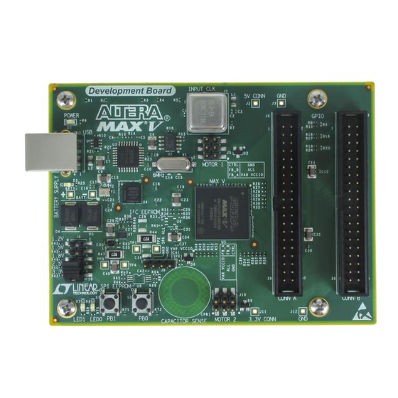
Page 8: Board Overview
2–2 Chapter 2: Board Components Board Overview Board Overview This section provides an overview of the MAX V CPLD development board, including an annotated board image and component descriptions. Figure 2–1 provides an overview of the development board features. Figure 2–1. Overview of the MAX V CPLD Development Board Features... -
Page 9: Featured Device: Max V Cpld
24-MHz input clock for the MAX II CPLD EPM240M100. Connectors J6, J7 GPIO headers Two general-purpose 2x40-pin 0.1-inch expansion headers. A 4-pin PC speaker header which connects to the MAX V CPLD I/O PC speaker header bank 2. J5, J10 DC motor headers Two motor headers which connects to the MAX V CPLD I/O bank 2. -
Page 10: I/O Resources
Table 2–4 lists the MAX V CPLD device pin count and usage by function on the development board. Table 2–4. MAX V CPLD Device I/O Pin Count and Usage (Part 1 of 2) Function I/O Standard I/O Count... -
Page 11: Configuration, Status, And Setup Elements
Chapter 2: Board Components 2–5 Configuration, Status, and Setup Elements Table 2–4. MAX V CPLD Device I/O Pin Count and Usage (Part 2 of 2) Function I/O Standard I/O Count Special Pins Push-Buttons Push-button 2: Dev_CLRn User LEDs — C EEPROM 3.3-V CMOS... -
Page 12: Cpld Configuration Using External Usb-Blaster
2 x 5 Header (Connector not mounted) The primary configuration mode for the MAX V CPLD is via JTAG using the MAX II configuration controller design (embedded USB-Blaster). The board also includes a JTAG connector which interfaces directly to the MAX V CPLD as the alternate source for configuration. -
Page 13: Setup Elements
To replace the clock input with a different frequency oscillator, unplug the current oscillator from the board and plug the desired oscillator into the 4-pin socket. Figure 2–4 shows the MAX V CPLD development board clock input. Figure 2–4. MAX V CPLD Development Board Clock Input 10 MHz... -
Page 14: Connectors
GPIO connector A pin AGPIO_23 J6.26 GPIO connector A pin AGPIO_24 J6.27 GPIO connector A pin AGPIO_25 J6.28 GPIO connector A pin AGPIO_26 J6.29 Power — 3.3VIN_CONN J6.30 Ground — — MAX V CPLD Development Board Reference Manual September 2015 Altera Corporation... - Page 15 GPIO connector B pin BGPIO_17 J7.20 GPIO connector B pin BGPIO_18 J7.21 GPIO connector B pin BGPIO_19 J7.22 GPIO connector B pin BGPIO_20 J7.23 GPIO connector B pin BGPIO_21 September 2015 Altera Corporation MAX V CPLD Development Board Reference Manual...
-
Page 16: Pc Speaker Header
The development board includes one PC speaker header which connects to the MAX V CPLD I/O bank 2. The speaker header also supports a compatible standard four-pin motherboard speaker. MAX V CPLD Development Board Reference Manual September 2015 Altera Corporation... -
Page 17: Dc Motor Headers
Note to Table 2–12: (1) This component is a compatible unit which can be used on the development board. The MAX V CPLD development kit does not include this component. DC Motor Headers The development board includes two DC motor headers which are driven by six open-drain I/Os from the MAX V CPLD. - Page 18 Note to Table 2–14: (1) This component is a compatible unit which can be used on the development board. The MAX V CPLD development kit does not include this component. MAX V CPLD Development Board Reference Manual September 2015 Altera Corporation...
-
Page 19: General User Input/Output
The development board includes two user-defined push-button switches. Board references S1 (USER_PB1) and S2 (USER_PB0) are push-button switches that allow you to interact with the MAX V CPLD device. There is no board-specific function for these user-defined push-button switches. Table 2–15 lists the user-defined push-button switch schematic signal names and their corresponding MAX V CPLD device pin numbers. -
Page 20: Off-Chip Eeprom
Table 2–19 lists the I C EEPROM device pin assignments, signal names, and functions. The signal names and types are relative to the MAX V CPLD device in terms of I/O setting and direction. Table 2–19. I C EEPROM Pin Assignments, Schematic Signal Names, and Functions... -
Page 21: Spi Eeprom
Note to Table 2–20: (1) This component is a compatible unit which can be used on the development board. The MAX V CPLD development kit does not include this component. SPI EEPROM Board reference U8 is a footprint to mount a SPI EEPROM device onto the development board. -
Page 22: Power Supply
(2) X* indicates that the concentration of the hazardous substance of at least one of all homogeneous materials in the parts is above the relevant threshold of the SJ/T11363-2006 standard, but it is exempted by EU RoHS. MAX V CPLD Development Board Reference Manual September 2015 Altera Corporation... -
Page 23: Additional Information
Product literature Website www.altera.com/literature Non-technical support (General) Email nacomp@altera.com (Software Licensing) Email authorization@altera.com Note to Table: (1) You can also contact your local Altera sales office or sales representative. September 2015 Altera Corporation MAX V CPLD Development Board Reference Manual... -
Page 24: Typographic Conventions
A warning calls attention to a condition or possible situation that can cause you injury. The envelope links to the Email Subscription Management Center page of the Altera website, where you can sign up to receive update notifications for Altera documents. MAX V CPLD Development Board Reference Manual September 2015 Altera Corporation...
Need help?
Do you have a question about the MAX V CPLD and is the answer not in the manual?
Questions and answers