
Related Manuals for Altera DE1


Summary of Contents for Altera DE1
-
Page 1: User Manual
Altera DE1 Board Development and Education Board User Manual Version 1.1 Copyright © 2006 Altera Corporation... -
Page 2: Table Of Contents
Control Panel Setup ......................10 Controlling the LEDs and 7-Segment Displays ..............12 SDRAM/SRAM Controller and Programmer..............13 Flash Memory Programmer ....................14 Overall Structure of the DE1 Control Panel ..............16 TOOLS – Multi-Port SRAM/SDRAM/Flash Controller ...........18 VGA Display Control......................19 Chapter 4 Using the DE1 Board .....................24 Configuring the Cyclone II FPGA ..................24... -
Page 3: Chapter 1 De1 Package
DE1 User Manual Chapter 1 DE1 Package The DE1 package contains all components needed to use the DE1 board in conjunction with a computer that runs the Microsoft Windows software. 1.1 Package Contents Figure 1.1 shows a photograph of the DE1 package. -
Page 4: The De1 Board Assembly
DE1 User Manual embedded processor • Bag of six rubber (silicon) covers for the DE1 board stands. The bag also contains some extender pins, which can be used to facilitate easier probing with testing equipment of the board’s I/O expansion headers •... -
Page 5: Chapter 2 Altera De1 Board
DE1 User Manual • Terasic Technologies No. 356, Sec. 1, Fusing E. Rd. Jhubei City, HsinChu County, Taiwan, 302 Email: support@terasic.com Web: www.de1.terasic.com Chapter 2 Altera DE1 Board This chapter presents the features and design characteristics of the DE1 board. -
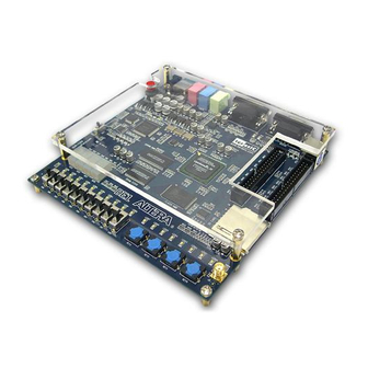
Page 6: Layout And Components
DE1 User Manual 2.1 Layout and Components A photograph of the DE1 board is shown in Figure 2.1. It depicts the layout of the board and indicates the location of the connectors and key components. Figure 2.1. The DE1 board. -
Page 7: Block Diagram Of The De1 Board
DE1 board. In order to use the DE1 board, the user has to be familiar with the Quartus II software. The necessary knowledge can be acquired by reading the tutorials Getting Started with Altera’s DE1 Board and Quartus II Introduction (which exists in three versions based on the design entry method used, namely Verilog, VHDL or schematic entry). - Page 8 • On-board USB Blaster for programming and user API control • JTAG and AS programming modes are supported SRAM • 512-Kbyte Static RAM memory chip • Organized as 256K x 16 bits • Accessible as memory for the Nios II processor and by the DE1 Control Panel SDRAM...
- Page 9 • Normally high; generates one active-low pulse when the switch is pressed Toggle switches • 10 toggle switches for user inputs • A switch causes logic 0 when in the DOWN (closest to the edge of the DE1 board) position and logic 1 when in the UP position Clock inputs •...
-
Page 10: Power-Up The De1 Board
4. Connect your headset to the Line-out audio port on the DE1 board 5. Turn the RUN/PROG switch on the left edge of the DE1 board to RUN position; the PROG position is used only for the AS Mode programming 6. - Page 11 • Set the toggle switch to the UP position and connect the output of an audio player to the Line-in connector on the DE1 board; on your headset you should hear the music played from the audio player (MP3, PC, iPod, or the like) •...
-
Page 12: Chapter 3 De1 Control Panel
Chapter 3 DE1 Control Panel The DE1 board comes with a Control Panel facility that allows a user to access various components on the board through a USB connection from a host computer. This chapter first presents some basic functions of the Control Panel, then describes its structure in block diagram form, and finally describes its capabilities. - Page 13 Figure 3.1. Quartus II Programmer window. Figure 3.2. The DE1 Control Panel. The concept of the DE1 Control Panel is illustrated in Figure 3.3. The IP that performs the control functions is implemented in the FPGA device. It communicates with the Control Panel window,...
-
Page 14: Controlling The Leds And 7-Segment Displays
Figure 3.3. The DE1 Control Panel concept. The DE1 Control Panel can be used to change the values displayed on 7-segment displays, light up LEDs, talk to the PS/2 keyboard, read/write the SRAM, Flash Memory and SDRAM, load an image pattern to display as VGA output, load music to the memory and play music via the audio DAC. -
Page 15: Sdram/Sram Controller And Programmer
3.3 SDRAM/SRAM Controller and Programmer The Control Panel can be used to write/read data to/from the SDRAM and SRAM chips on the DE1 board. We will describe how the SDRAM may be accessed; the same approach is used to access the SRAM. -
Page 16: Flash Memory Programmer
3.4 Flash Memory Programmer The Control Panel can be used to write/read data to/from the Flash memory chip on the DE1 board. It can be used to: • Erase the entire Flash memory... - Page 17 • The time required to erase the entire Flash memory is about 20 seconds. Do not close the DE1 Control Panel in the middle of the operation. To open the Flash memory control window, shown in Figure 3.6, select the FLASH tab in the Control Panel.
-
Page 18: Overall Structure Of The De1 Control Panel
3.5 Overall Structure of the DE1 Control Panel The DE1 Control Panel facility communicates with a circuit that is instantiated in the Cyclone II FPGA. This circuit is specified in Verilog code, which makes it possible for a knowledgeable user to change the functionality of the Control Panel. - Page 19 C++, a USB command controller, and a multi-port SRAM/SDRAM/Flash controller. Figure 3.7. The DE1 Control Panel block diagram. Users can connect circuits of their own design to one of the User Ports of the SRAM/SDRAM/Flash controller.
-
Page 20: Tools - Multi-Port Sram/Sdram/Flash Controller
Flash memory. You can use the file music.wav in the directory DE1_demonstrations\music on the DE1 System CD-ROM. 2. In the DE1 Control Panel, select the TOOLS tab to reach the window in Figure 3.8. Figure 3.8. TOOLS window of the DE1 Control Panel. -
Page 21: Vga Display Control
• Make sure that the checkboxes Default Image and Cursor Enable are checked. • Connect a VGA monitor to the DE1 board and you should see on the screen the default image shown in Figure 3.9. The image includes a cursor which can be controlled by means of the X/Y-axes scroll bars on the DE1 Control Panel. - Page 22 Another image is provided in the file picture.dat in the folder DE1_demonstrations\pictures on the DE1 System CD-ROM. You can display this image as follows: • Select the SRAM page of the Control Panel and load the file picture.dat into the SRAM.
- Page 23 DE1 User Manual Figure 3.11. Multi-Port Controller configured to display an image from the SRAM. Figure 3.12. A displayed image. You can display any image file by loading it into the SRAM chip or into an M4K memory block in the Cyclone II chip.
- Page 24 File Name field in the displayed window. 6. Raw_Data_Gray.dat is the raw data that can be downloaded directly into the SRAM on the DE1 board and displayed on the VGA monitor using the VGA controller IP described in the DE1_USB_API project.
- Page 25 DE1 User Manual Image Source R/G/B Band B&W Output Result Filter Threshold (640x480) Filter Color Picture R/G/B Raw_Data_Gray Color Picture R/G/B BW Threshold Raw_Data_BW + (optional) Raw_Data_BW.txt Grayscale Raw_Data_Gray Picture Grayscale BW Threshold Raw_Data_BW + Picture Raw_Data_BW.txt Note: Raw_Data_BW.txt is used to fill in the MIF/Intel Hex format for M4K SRAM...
-
Page 26: Chapter 4 Using The De1 Board
This chapter gives instructions for using the DE1 board and describes each of its I/O devices. 4.1 Configuring the Cyclone II FPGA The procedure for downloading a circuit from a host computer to the DE1 board is described in the tutorial Quartus II Introduction. This tutorial is found in the DE1_tutorials folder on the DE1 System CD-ROM, and it is also available on the Altera DE1 web pages. - Page 27 • Ensure that power is applied to the DE1 board • Connect the supplied USB cable to the USB Blaster port on the DE1 board (see Figure 2.1) • Configure the JTAG programming circuit by setting the RUN/PROG switch (on the left side of the board) to the RUN position.
-
Page 28: Using The Leds And Switches
Figure 4.2. The AS configuration scheme. In addition to its use for JTAG and AS programming, the USB Blaster port on the DE1 board can also be used to control some of the board's features remotely from a host computer. Details that describe this method of using the USB Blaster port are given in Chapter 3. - Page 29 DE1 User Manual There are 27 user-controllable LEDs on the DE1 board. Eighteen red LEDs are situated above the 18 toggle switches, and eight green LEDs are found above the pushbutton switches (the 9 green LED is in the middle of the 7-segment displays). Each LED is driven directly by a pin on the Cyclone II FPGA;...
- Page 30 DE1 User Manual Figure 4.5. Schematic diagram of the LEDs. Signal Name FPGA Pin No. Description SW[0] PIN_L22 Toggle Switch[0] SW[1] PIN_L21 Toggle Switch[1] SW[2] PIN_M22 Toggle Switch[2] SW[3] PIN_V12 Toggle Switch[3] SW[4] PIN_W12 Toggle Switch[4] SW[5] PIN_U12 Toggle Switch[5]...
- Page 31 DE1 User Manual SW[8] PIN_M1 Toggle Switch[8] SW[9] PIN_L2 Toggle Switch[9] Table 4.1. Pin assignments for the toggle switches. Signal Name FPGA Pin No. Description KEY[0] PIN_R22 Pushbutton[0] KEY[1] PIN_R21 Pushbutton[1] KEY[2] PIN_T22 Pushbutton[2] KEY[3] PIN_T21 Pushbutton[3] Table 4.2. Pin assignments for the pushbutton switches.
-
Page 32: Using The 7-Segment Displays
DE1 User Manual 4.3 Using the 7-segment Displays The DE1 Board has four 7-segment displays. These displays are arranged into a group of four, with the intent of displaying numbers of various sizes. As indicated in the schematic in Figure 4.6, the seven segments are connected to pins on the Cyclone II FPGA. -
Page 33: Clock Inputs
Seven Segment Digit 3[6] Table 4.4. Pin assignments for the 7-segment displays. 4.4 Clock Inputs The DE1 board includes three oscillators that produce 27 MHz, 24Mhz, and 50 MHz clock signals. The board also includes an SMA connector which can be used to connect an external clock source to the board. -
Page 34: Using The Expansion Header
Table 4.5. Pin assignments for the clock inputs. 4.5 Using the Expansion Header The DE1 Board provides two 40-pin expansion headers. Each header connects directly to 36 pins on the Cyclone II FPGA, and also provides DC +5V (VCC5), DC +3.3V (VCC33), and two GND pins. - Page 35 DE1 User Manual Figure 4.10. Schematic diagram of the expansion headers. Signal Name FPGA Pin No. Description GPIO_0[0] PIN_A13 GPIO Connection 0[0]...
- Page 36 DE1 User Manual GPIO_0[1] PIN_B13 GPIO Connection 0[1] GPIO_0[2] PIN_A14 GPIO Connection 0[2] GPIO_0[3] PIN_B14 GPIO Connection 0[3] GPIO_0[4] PIN_A15 GPIO Connection 0[4] GPIO_0[5] PIN_B15 GPIO Connection 0[5] GPIO_0[6] PIN_A16 GPIO Connection 0[6] GPIO_0[7] PIN_B16 GPIO Connection 0[7] GPIO_0[8] PIN_A17...
- Page 37 DE1 User Manual GPIO_1[2] PIN_H14 GPIO Connection 1[2] GPIO_1[3] PIN_G15 GPIO Connection 1[3] GPIO_1[4] PIN_E14 GPIO Connection 1[4] GPIO_1[5] PIN_E15 GPIO Connection 1[5] GPIO_1[6] PIN_F15 GPIO Connection 1[6] GPIO_1[7] PIN_G16 GPIO Connection 1[7] GPIO_1[8] PIN_F12 GPIO Connection 1[8] GPIO_1[9] PIN_F13...
-
Page 38: Using Vga
DE1 User Manual 4.6 Using VGA The DE1 board includes a 16-pin D-SUB connector for VGA output. The VGA synchronization signals are provided directly from the Cyclone II FPGA, and a 4-bit DAC using resistor network is used to produce the analog data signals (red, green, and blue). The associated schematic is given in Figure 4.11 and can support standard VGA resolution (640x480 pixels, at 25 MHz). - Page 39 DE1 User Manual During the data display interval the RGB data drives each pixel in turn across the row being displayed. Finally, there is a time period called the front porch (d) where the RGB signals must again be off before the next hsync pulse can occur. The timing of the vertical synchronization (vsync) is the same as shown in Figure 4.12, except that a vsync pulse signifies the end of one frame and the...
-
Page 40: Using The 24-Bit Audio Codec
Table 4.8. ADV7123 pin assignments. 4.7 Using the 24-bit Audio CODEC The DE1 board provides high-quality 24-bit audio via the Wolfson WM8731 audio CODEC (enCOder/DECoder). This chip supports microphone-in, line-in, and line-out ports, with a sample rate adjustable from 8 kHz to 96 kHz. The WM8731 is controlled by a serial I2C bus interface, which is connected to pins on the Cyclone II FPGA. -
Page 41: Rs-232 Serial Port
For detailed information on how to use the transceiver refer to the datasheet, which is available on the manufacturer’s web site, and from the Datasheet folder on the DE1 System CD-ROM. Figure 4.16 shows the related schematics, and Table 4.10 lists the Cyclone II FPGA pin assignments. -
Page 42: Ps/2 Serial Port
DE1 User Manual 4.9 PS/2 Serial Port The DE1 board includes a standard PS/2 interface and a connector for a PS/2 keyboard or mouse. Figure 4.17 shows the schematic of the PS/2 circuit. Instructions for using a PS/2 mouse or keyboard can be found by performing an appropriate search on various educational web sites. - Page 43 DE1 User Manual Figure 4.23. SDRAM schematic. Figure 4.24. SRAM schematic.
- Page 44 DE1 User Manual Figure 4.25. Flash schematic. Signal Name FPGA Pin No. Description DRAM_ADDR[0] PIN_W4 SDRAM Address[0] DRAM_ADDR[1] PIN_W5 SDRAM Address[1] DRAM_ADDR[2] PIN_Y3 SDRAM Address[2] DRAM_ADDR[3] PIN_Y4 SDRAM Address[3] DRAM_ADDR[4] PIN_R6 SDRAM Address[4] DRAM_ADDR[5] PIN_R5 SDRAM Address[5] DRAM_ADDR[6] PIN_P6 SDRAM Address[6]...
- Page 45 DE1 User Manual DRAM_DQ[7] PIN_Y2 SDRAM Data[7] DRAM_DQ[8] PIN_N1 SDRAM Data[8] DRAM_DQ[9] PIN_N2 SDRAM Data[9] DRAM_DQ[10] PIN_P1 SDRAM Data[10] DRAM_DQ[11] PIN_P2 SDRAM Data[11] DRAM_DQ[12] PIN_R1 SDRAM Data[12] DRAM_DQ[13] PIN_R2 SDRAM Data[13] DRAM_DQ[14] PIN_T1 SDRAM Data[14] DRAM_DQ[15] PIN_T2 SDRAM Data[15] DRAM_BA_0...
- Page 46 DE1 User Manual SRAM_ADDR[14] PIN_R10 SRAM Address[14] SRAM_ADDR[15] PIN_T7 SRAM Address[15] SRAM_ADDR[16] PIN_Y6 SRAM Address[16] SRAM_ADDR[17] PIN_Y5 SRAM Address[17] SRAM_DQ[0] PIN_AA6 SRAM Data[0] SRAM_DQ[1] PIN_AB6 SRAM Data[1] SRAM_DQ[2] PIN_AA7 SRAM Data[2] SRAM_DQ[3] PIN_AB7 SRAM Data[3] SRAM_DQ[4] PIN_AA8 SRAM Data[4] SRAM_DQ[5]...
- Page 47 DE1 User Manual FL_ADDR[8] PIN_R14 FLASH Address[8] FL_ADDR[9] PIN_Y13 FLASH Address[9] FL_ADDR[10] PIN_R12 FLASH Address[10] FL_ADDR[11] PIN_T12 FLASH Address[11] FL_ADDR[12] PIN_AB14 FLASH Address[12] FL_ADDR[13] PIN_AA13 FLASH Address[13] FL_ADDR[14] PIN_AB13 FLASH Address[14] FL_ADDR[15] PIN_AA12 FLASH Address[15] FL_ADDR[16] PIN_AB12 FLASH Address[16] FL_ADDR[17]...
-
Page 48: Chapter 5 Examples Of Advanced Demonstrations
4. When fixpaths is finished, press any key to complete the process. 5.1 DE1 Factory Configuration The DE1 board is shipped from the factory with a default configuration that demonstrates some of the basic features of the board. The setup required for this demonstration, and the locations of its files are shown below. -
Page 49: Music Synthesizer Demonstration
PS/2 Keyboard and a speaker. Figure 5.1 shows the setup of the demonstration. PS/2 Keyboard is used as the piano keyboard for input. The Cyclone II FPGA on the DE1 board serves as the Music Synthesizer SOC to generate music and tones. The VGA connected to the DE1 board is used to show which key is pressed during the playing of the music. - Page 50 DE1 User Manual The audio codec used on the DE1 board has two channels, which can be turned ON/OFF using SW1 and SW2. Figure 5.1. The Setup of the Music Synthesizer Demonstration. Figure 5.2. Block diagram of the Music Synthesizer design...
- Page 51 • Bit stream used: DE1_Synthesizer.sof or DE1_Synthesizer.pof • Connect a PS/2 Keyboard to the DE1 board. • Connect the VGA output of the DE1 board to a VGA monitor (both LCD and CRT type of monitors should work) • Connect the Lineout of the DE1 board to a speaker.
-
Page 52: A Karaoke Machine
Figure 5.3. Usage of the Key 5.3 A Karaoke Machine This demonstration uses the microphone-in, line-in, and line-out ports on the DE1 board to create a Karaoke Machine application. The Wolfson WM8731 audio CODEC is configured in the master mode, where the audio CODEC generates AD/DA serial bit clock (BCK) and the left/right channel clock (LRCK) automatically. - Page 53 • Project directory: DE1_i2sound • Bit stream used: i2sound.sof or i2sound.pof • Connect a microphone to the microphone-in port (pink color) on the DE1 board • Connect the audio output of a music-player, such as an MP3 player or computer, to the line-in port (blue color) on the DE1 board •...
-
Page 54: Sd Card Music Player
DE1 board. In this demonstration we show how to implement an SD Card Music Player on the DE1 board, in which the music files are stored in an SD card and the board can play the music files via its CD-quality audio DAC circuits. - Page 55 • Load the bit stream into the FPGA • Run the Nios II IDE under the workspace DE1_SD_Card_Audio • Connect a headset or speaker to the DE1 board and you should be able to hear the music played from the SD Card Figure 5.12 illustrates the setup for this demonstration.
- Page 56 Altera Corporation in the U.S. and other countries. All other product or service names are the property of their respective holders. Altera products are protected under numerous U.S.
Need help?
Do you have a question about the DE1 and is the answer not in the manual?
Questions and answers