
Related Manuals for Altera MAX 10 FPGA 10M50


Summary of Contents for Altera MAX 10 FPGA 10M50
- Page 1 MAX 10 FPGA 10M50 Evaluation Kit User Guide 101 Innovation Drive UG-20006 Subscribe 2016.02.29 San Jose, CA 95134 Send Feedback www.altera.com...
-
Page 2: Table Of Contents
TOC-2 Contents MAX 10 FPGA 10M50 Evaluation Kit Overview..........1-1 Board Component Blocks...........................1-1 Supported Items Not Included with the Kit.....................1-3 Getting Started....................2-1 Powering the Kit............................2-1 Installing the USB-Blaster Driver......................2-1 Handling the Kit............................2-1 Factory Default Switch and Jumper Settings....................2-2 Board Components....................3-1 Board Overview............................3-1... -
Page 3: Max 10 Fpga 10M50 Evaluation Kit Overview
Altera assumes no responsibility or liability arising out of the application or use of any information, product, or service described herein except as expressly agreed to in writing by Altera. Altera customers are advised to obtain the latest version of device specifications before relying on any published information and before placing orders for products or services. - Page 4 • Free Quartus Prime Lite Edition design software (download software and license from ® www.altera.com/download • Complete documentation • User Guide, bill of material, schematic and board files MAX 10 FPGA 10M50 Evaluation Kit Overview Altera Corporation Send Feedback...
-
Page 5: Supported Items Not Included With The Kit
Manufacturer Website Reference Part Number J1, J2 www.parlex.com Cable Flat Flex Top / Parlex 050R36-76B Top 36 POS 0.5 MM Molex 0210200385 www.molex.com pitch www.leopardi‐ Leopard Imaging LI-FLEX03 maging.com MAX 10 FPGA 10M50 Evaluation Kit Overview Altera Corporation Send Feedback... - Page 6 Leopard Imaging LI-USB30- Daughter Card maging.com MIPI-TESTER LI-CAM-OV10640-MIPI Leopard Imaging LI_CAM- http://shop.leopardi‐ Daughter Card OV10640-MIPI maging.com MIPI 5MP AF Camera http://shop.udoo.org UDOO MIPI 5MP IR Daughter Card AF Camera MAX 10 FPGA 10M50 Evaluation Kit Overview Altera Corporation Send Feedback...
-
Page 7: Getting Started
Altera assumes no responsibility or liability arising out of the application or use of any information, product, or service described herein except as expressly agreed to in writing by Altera. Altera customers are advised to obtain the latest version of device specifications before relying on any published information and before placing orders for products or services. -
Page 8: Factory Default Switch And Jumper Settings
HIGH (OFF =1) SW1.3 USER_DIPSW2 User-Defined HIGH (OFF =1) SW1.4 USER_DIPSW3 User-Defined HIGH (OFF =1) Table 2-2: Default SW2 DIP Switch Settings Board Reference Signal Name Function Default Position SW2.1 USER_DIPSW4 User-Defined HIGH (OFF =1) Getting Started Altera Corporation Send Feedback... - Page 9 Pins 1 and 2 power option when R292 and R293 not installed J11[2-3] Jumper for board USB power Pins 2 and 3 option when R292 and R293 not installed. This is the default power jumper position. Getting Started Altera Corporation Send Feedback...
-
Page 10: Board Components
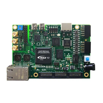
Altera assumes no responsibility or liability arising out of the application or use of any information, product, or service described herein except as expressly agreed to in writing by Altera. Altera customers are advised to obtain the latest version of device specifications before relying on any published information and before placing orders for products or services. - Page 11 UG-20006 Board Overview 2016.02.29 Figure 3-1: Overview of the MAX 10 10M50 FPGA Evaluation Kit Features - Board Image (Front View) Board Components Altera Corporation Send Feedback...
- Page 12 MAX 10 FPGA 10M50DAF484C6GES, 50K LEs, F484 package, -6ES speed grade. CPLD MAX II EPM1270 256-MBGA, 2.5V/3.3V, VCCINT for On-Board USB-Blaster II. Power Regulator Enpirion EN5329QI 2A PowerSoC Low Profile Synchronous Buck DC-DC Converter with Integrated Inductor. Board Components Altera Corporation Send Feedback...
- Page 13 Programmable Clock Four channel programmable oscillator with default frequencies of 24, 24, 125,100 MHz. 50-MHz oscillator 50-MHz crystal oscillator for general purpose logic of MAX 10 and MAX II devices. General User Input and Output Board Components Altera Corporation Send Feedback...
- Page 14 Power switch When using DC power adapter, switch to power on or off the board when power is supplied from the DC input jack. DC adapter and USB power don't work at the same time. Board Components Altera Corporation Send Feedback...
-
Page 15: Featured Device: Max 10 Fpga
• Ensure that the Quartus II Programmer and the USB-Blaster driver are installed on the host computer • The USB cable is connected to the kit • Power to the board is on, and no other applications that use the JTAG chain are running. Board Components Altera Corporation Send Feedback... -
Page 16: Selecting The Internal Configuration Scheme
Table 3-3: Status LED Signal Names Board Reference Signal Name Colour Device/Pin Number I/O Standard MAXII_CONF_ Green MAX II / Y10 3.3 V DONE 5V_LED_R Yellow 2.5V_LED_R Yellow 1.2V_LED Yellow MAX II / Y9 3.3 V Board Components Altera Corporation Send Feedback... -
Page 17: Setup Elements
MAX10_nCONFIG 3.3V MAX10_RESETn 3.3V General User Input/Output User-defined I/O signal names, FPGA pin numbers, and I/O standards for the MAX 10 FPGA 10M50 Evaluation Board. Table 3-6: User-Defined Push Button Signal Names Board Reference Signal Name MAX 10 FPGA Pin... - Page 18 LVDS channels J12.6 USER_LVDS_N2 AA17 DIFFIO_TX_RX_ LVDS User I/O_2. Note 1 B43N, High Speed J12.7 ---- ---- Ground Reference for this group of I/Os J12.8 ---- ---- Ground Reference for this group of I/Os Board Components Altera Corporation Send Feedback...
- Page 19 I/Os J13.1 2.5V Power ---- ---- Power Supply for Connector J13 J13.2 2.5V Power ---- ---- Power Supply for Connector J13 J13.3 USER_LVDS_P5 DIFFIO_TX_RX_ LVDS User I/O_5. Note 1 B7p, High Speed Board Components Altera Corporation Send Feedback...
- Page 20 DIFFIO_TX_RX_ LVDS User I/O_7. Note 1 B5n, High Speed J13.18 ---- ---- Not Connected J13.19 ---- ---- Ground Reference for this group of I/Os J13.20 ---- ---- Ground Reference for this group of I/Os Board Components Altera Corporation Send Feedback...
- Page 21 I/Os J14.13 USER_IO4 DIFFIO_RX_T5p, User I/O_4 High Speed J14.14 USER_IO9 DIFFIO_RX_T2p, User I/O_9 High Speed Note: 1. Termination resistors are required to be installed by the user for proper high speed LVDS I/O use. Board Components Altera Corporation Send Feedback...
-
Page 22: Clock Circuitry
Clock Circuitry 2016.02.29 Clock Circuitry The MAX 10 FPGA 10M50 Evaluation Board includes two oscillators: • A four channel programmable oscillator with default frequency of 24-MHz, 24-MHz, 125-MHz, 100- MHz. • A two channel crystal oscillator with default frequency of 50-MHz. -
Page 23: Off-Board Clock Input/Output
GPIO CLKOUT_LVDS_ 2.5 V Single-ended clock output, or positive terminal for differential clock output to user GPIO CLKOUT_LVDS_ 2.5 V Single-ended clock output, or negative terminal for differential clock output to user GPIO Board Components Altera Corporation Send Feedback... -
Page 24: Clock Control Gui
FPGA using the Quartus II Programmer. The Clock Control The MAX 10 FPGA 10M50 Evaluation Board Clock Control application sets the programmable oscillators to any frequency between 10 MHz and 200 MHz. It communicates with the MAX II device on the board through the JTAG bus. -
Page 25: Components And Interfaces
Sets the programmable oscillator frequency for the selected clock to the value in the CLK0 and CLK3 controls. Frequency changes might take several milliseconds to take effect. You might see glitches on the clock during this time. Altera recommends resetting the FPGA logic after changing frequen‐ cies. - Page 26 3.3 V HDMI digital video data DIN17 U3.42 HDMI_VIDEO_ 3.3 V HDMI digital video data DIN18 U3.41 HDMI_VIDEO_ 3.3 V HDMI digital video data DIN19 U3.40 HDMI_VIDEO_ 3.3 V HDMI digital video data DIN20 Board Components Altera Corporation Send Feedback...
-
Page 27: Pmod Connectors
In/Out PMODA_D2 PMODA_IO2 3.3 V In/Out PMODA_D3 PMODA_IO3 3.3 V In/Out PMODA_D4 PMODA_IO4 3.3 V In/Out PMODA_D5 PMODA_IO5 3.3 V In/Out PMODA_D6 PMODA_IO6 3.3 V In/Out PMODA_D7 PMODA_IO7 3.3 V In/Out 3.3 V Power Board Components Altera Corporation Send Feedback... -
Page 28: Memory
FPGA. A soft IP memory controller is required as part of the FPGA design. The memory controller can be a user supplied IP or IP available for purchase from Intel PSG (formerly Altera) or a partner. LPDDR2 The MAX 10 FPGA provides full-speed support to a x16 LPDDR2 200-MHz interface by using a 1Gbit x 16 memory. - Page 29 Data Bus Byte Lane 1 U2.F8 LPDDR2_DQ14 1.2V HSUL Data Bus Byte Lane 1 U2.E8 LPDDR2_DQ15 1.2V HSUL Data Bus Byte Lane 1 U2.L6 LPDDR2_DQS0 Differential 1.2V Data Strobe P Byte Lane 0 HSUL Board Components Altera Corporation Send Feedback...
-
Page 30: Flash
.INI variable. Flash The MAX 10 10M50 Evaluation Kit provides a 512-Mb (megabit) quad SPI flash memory. Altera Generic QUAD SPI controller core is used by default to erase, read, and write quad SPI flash in reference designs of the Board Test System (BTS) installer. -
Page 31: Mipi Csi-2 Transmitter
MIPI-USB3-Tester module. This module includes one MIPI clock channel and four MIPI data channels. To interface the CSI-2 D-PHY compliant I/Os, the MAX 10 FPGA 10M50 Evaluation Kit uses one 1.8V HSTL signal pair and one 2.5V LVCMOS signal pair to support both high-speed and low-power nodes of one MIPI clock or data lane. - Page 32 Lane3 (low power, positive terminal) J1.19 MAX_TX_DATA_HS_N3 MAX 10/ U1 1.8V HSTL Differential output data Lane3 (high speed, negative terminal) J1.20 MAX_TX_DATA_LP_P3 MAX 10/ AB5 2.5V LVCMOS Differential output data Lane3 (low power, positive terminal) Board Components Altera Corporation Send Feedback...
- Page 33 MAX 10/ U4 1.8V LVCMOS GPIO3 J1.6 MIPI_TX_GPIO4 MAX 10/ U5 1.8V LVCMOS GPIO4 J1.5 MIPI_TX_GPIO5 MAX 10/ V3 1.8V LVCMOS GPIO5 J1.33, 1.8V_MIPITX ---- 1.8V 1.8V J1.32 J1.36, 3.3V_MIPITX ---- 3.3V 3.3V J1.35, J1.34 Board Components Altera Corporation Send Feedback...
-
Page 34: Mipi Csi-2 Receiver
Altera) sales team for assistance or check the DesignStore. MIPI CSI-2 Receiver The MAX 10 FPGA 10M50 Evaluation Kit supports MIPI CSI-2 receiver D-PHY to both Leopard Imaging OV10640 and UDOO OV5640 modules. The OV10640 module includes one MIPI clock channel and four MIPI data channels, while the OV5640 module has one MIPI clock channel and two MIPI data channels. - Page 35 Lane3 (low power, positive terminal) J2.18 OV0640_DATA_ MAX 10/W22 1.2V HSTL Differential input data LP_N3 Lane3 (low power, negative terminal) J2.20 OV10640_DATA_ MAX 10/AA16 2.5V LVDS Differential input data HS_P4 Lane4 (high speed, positive terminal) Board Components Altera Corporation Send Feedback...
- Page 36 J2.32 OV10640_FSIN MAX 10/P8 1.8V LVCMOS Frame sync input J2.4, J2.5 1.8V ---- 1.8V 1.8V J2.1, J2.2, J2.3 3.3V ---- 3.3V 3.3V J2.6, J2.7, J2.10, ---- J2.13, J2.16, J2.19, J2.22, J2.29, J2.33, J2.34 Board Components Altera Corporation Send Feedback...
- Page 37 MAX 10/P15 1.2V HSTL Differential input data LP_P2 Lane2 (low power,positive terminal) J3.1 OV5640_DATA_ MAX 10/P14 1.2V HSTL Differential input data LP_N2 Lane2 (low power,negative terminal) J3.13 OV5640_SDC MAX 10/M3 3.3V LVCMOS Control Bus Clock Board Components Altera Corporation Send Feedback...
-
Page 38: Power Supply
Resistors R292 and R293 are designed for hard wiring the power selection. J11 must not be used when either R292 or R293 is populated. Power Up Sequence The figure below shows the power distribution system on the MAX 10 FPGA 10M50 Evaluation Board. Board Components Altera Corporation... - Page 39 UG-20006 3-30 Power Up Sequence 2016.02.29 Figure 3-5: Power Tree The power up sequence of the MAX 10 FPGA 10M50 Evaluation Board is shown in the table below: Table 3-22: Power Up Sequence Table Power Up Sequence Device Output Voltage EP5358HUI 1.8V...
-
Page 40: Additional Information
Altera assumes no responsibility or liability arising out of the application or use of any information, product, or service described herein except as expressly agreed to in writing by Altera. Altera customers are advised to obtain the latest version of device specifications before relying on any published information and before placing orders for products or services. - Page 41 Mouser Electronics Authorized Distributor Click to View Pricing, Inventory, Delivery & Lifecycle Information: Intel EK-10M50F484...
Need help?
Do you have a question about the MAX 10 FPGA 10M50 and is the answer not in the manual?
Questions and answers