Altera Cyclone III Reference Manual
Fpga starter board
Hide thumbs
Also See for Cyclone III:
- Reference manual (91 pages) ,
- User manual (34 pages) ,
- Getting started manual (34 pages)

Related Manuals for Altera Cyclone III


Summary of Contents for Altera Cyclone III
- Page 1 Cyclone III FPGA Starter Board Reference Manual 101 Innovation Drive San Jose, CA 95134 www.altera.com Document Version: Document Date: April 2012...
- Page 2 © 2012 Altera Corporation. All rights reserved. ALTERA, ARRIA, CYCLONE, HARDCOPY, MAX, MEGACORE, NIOS, QUARTUS and STRATIX are Reg. U.S. Pat. & Tm. Off. and/or trademarks of Altera Corporation in the U.S. and other countries. All other trademarks and service marks are the property of their respective holders as described at www.altera.com/common/legal.html.
-
Page 3: Table Of Contents
Parallel Flash ........................... 2–13 DDR SDRAM ..........................2–15 SSRAM ............................. 2–17 Power Supply ............................2–19 Statement of China-RoHS Compliance .................... 2–20 Additional Information Revision History ..........................Info–i How to Contact Altera ........................Info–i Typographic Conventions ......................Info–ii Altera Corporation April 2012 Preliminary... - Page 4 Contents Stratix Device Handbook, Volume 1 Altera Corporation Preliminary April 2012...
-
Page 5: Chapter 1. Introduction
High Speed Mezzanine Card (HSMC) connector. For the latest information about available HMSC daughtercards, go to www.altera.com/products/devkits/kit-index.html. The main features of the Cyclone III starter board are: ■ Low-power consumption Altera Cyclone III EP3C25 chip in a 324-pin FineLine BGA (FBGA) package ■... -
Page 6: Board Component Blocks
Four PLLs ● 214 I/Os ● ■ Clock management system One 50-MHz clock oscillator to support a variety of protocols ● The Cyclone III device distributes the following clocks from its ● on-board PLLs: • DDR clock • SSRAM clock •... -
Page 7: Block Diagram
Introduction Block Diagram Figure 1–1 shows a functional block diagram of the Cyclone III FPGA starter board. Figure 1–1. Cyclone III FPGA Starter Board HSMC Switches Parallel Flash 16MB Cyclone III EP3C25F324 LEDs SSRAM Blaster 32MB Handling the When handling the board, it is important to observe the following... - Page 8 Handling the Board 1–4 Altera Corporation Cyclone III FPGA Starter Board Reference Manual April 2012...
-
Page 9: Chapter 2. Board Components And Interfaces
The board schematics, physical layout database, and ® manufacturing files for the Cyclone III FPGA starter board are included in the Cyclone III FPGA Starter Kit in the following directory: <install path>\cycloneIII_3c25_start\board_design_files For information on powering-up the Cyclone III FPGA starter board and installing the demonstration software, refer to the Cyclone III FPGA Starter Kit User Guide. - Page 10 Board Overview Figure 2–1 shows the top view of the Cyclone III FPGA starter board. Figure 2–1. Top View of the Cyclone III FPGA Starter Board FPGA Core Power 2.5 V I/O Power Measurement (JP6) Measurement (JP3) 1-MB SSRAM (U5)
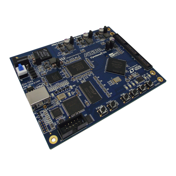
- Page 11 Board Components and Interfaces Figure 2–2 shows the diagonal view of the Cyclone III FPGA starter board. Figure 2–2. Diagonal View of the Cyclone III FPGA Starter Board Altera Corporation 2–3 April 2012 Cyclone III FPGA Starter Board Reference Manual...
- Page 12 Board Overview Table 2–1 describes the components and lists their corresponding board references. Table 2–1. Cyclone III FPGA Starter Board (Part 1 of 2) Component/ Type Board Reference Description Page Interface Featured Device FPGA Cyclone III EP3C25F324-C8, 324-pin FBGA package 2–5...
-
Page 13: Featured Device
Probe point Current sense Measure 2.5-V I/O power (shared between resistor devices) with current sense resistor. Featured The Cyclone III FPGA Starter Kit features the EP3C25F324 device (U1) in a 324-pin FineLine BGA (FBGA) package. Table 2–2 lists Cyclone III Device device features. -
Page 14: Clocking Circuitry
Table 2–3: The Cyclone III EP3C25F324 only supports one I/O standard in an I/O bank. I/O banks 3 and 4 are shared among the DDR, HSMC and LEDs. In several DDR designs, some of the I/O pins that share the same banks with the DDR are unavailable for use due to different I/O standards. -
Page 15: Jumpers
Figure 2–3 shows the simplest clocking scheme with a single clock input; however, much more complex clocking schemes can be implemented with Cyclone III FPGAs. Figure 2–3. Cyclone III FPGA Starter Board’s Clocking Scheme 16 MB Parallel Flash SSRAM B9, V9... -
Page 16: Interfaces
Removing the shunt enables the embedded USB-Blaster circuitry. When the shunt is in place, use any external cable such as the ByteBlaster II, EthernetBlaster, or USB-Blaster cable to configure the Cyclone III device. (The board ships without the JTAG header populated.) Interfaces This section describes the following Cyclone III FPGA starter board’s... -
Page 17: Hsmc Expansion Connector
Table 2–6 lists the ordering codes and shows the relationship between the standard Samtec Q-series connectors and the modified parts’ ordering codes. Table 2–6. Altera-Specific & Standard Samtec Part Numbers Altera-Specific Samtec Standard Samtec Part Part Number Number... -
Page 18: General User Interfaces
DP Bank .036 REF .006 REF General User Interfaces To allow you to fully use the I/O capabilities of the Cyclone III device, the following user interfaces are available on the board (remaining I/Os are connected to additional board resources): ■... -
Page 19: Push-Buttons
User Reset Push-Buttons The user reset push-button is an input to the Cyclone III device. This push-button is intended to be the master reset signal for the FPGA designs loaded into the Cyclone III device. The user reset push-button is connected to the DEV_CLRn pin on the FPGA. -
Page 20: Leds
Interfaces User Push-Buttons The four user push-buttons are intended for use in controlling FPGA designs loaded into the Cyclone III device. There is no board-specific function for these four push-buttons. LEDs The board has user LEDs and board-specific LEDs. Table 2–10 lists both user and board-specific LED pinout. -
Page 21: Memory
■ DDR SDRAM ■ SSRAM Parallel Flash The Cyclone III starter board has a 8M x 16 low voltage parallel flash. Table 2–11 lists the parallel flash board reference and manufacturing information. Table 2–11. Parallel Flash Manufacturing Information Board Reference... - Page 22 Bidirectional 2.5 V flash_sram_dq6 Bidirectional 2.5 V flash_sram_dq7 Bidirectional 2.5 V flash_sram_dq8 Bidirectional 2.5 V flash_sram_dq9 Bidirectional 2.5 V flash_sram_dq10 Bidirectional 2.5 V flash_sram_dq11 Bidirectional 2.5 V flash_sram_dq12 2–14 Altera Corporation Cyclone III FPGA Starter Board Reference Manual April 2012...
-
Page 23: Ddr Sdram
(dclk) Output 2.5 V flash_wait DDR SDRAM The Cyclone III FPGA starter board has a 4M x 16 x 4 DDR SDRAM. Table 2–13 lists DDR SDRAM board reference and manufacturing information. Table 2–13. DDR SDRAM Manufacturing Information Board Reference... - Page 24 Bidirectional SSTL-2 ddr_dq6 Bidirectional SSTL-2 ddr_dq7 Bidirectional SSTL-2 ddr_dq8 Bidirectional SSTL-2 ddr_dq9 Bidirectional SSTL-2 ddr_dq10 Bidirectional SSTL-2 ddr_dq11 Bidirectional SSTL-2 ddr_dq12 Bidirectional SSTL-2 ddr_dq13 Bidirectional SSTL-2 ddr_dq14 2–16 Altera Corporation Cyclone III FPGA Starter Board Reference Manual April 2012...
-
Page 25: Ssram
2–14: The Cyclone III EP3C25F324 only supports one I/O standard in an I/O bank. I/O banks 3 and 4 are shared among the DDR, HSMC and LEDs. In several DDR designs, some of the I/O pins that share the same banks with the DDR are unavailable for use due to different I/O standards. - Page 26 Bidirectional 2.5 V flash_sram_dq18 Bidirectional 2.5 V flash_sram_dq19 Bidirectional 2.5 V flash_sram_dq20 Bidirectional 2.5 V flash_sram_dq21 Bidirectional 2.5 V flash_sram_dq22 Bidirectional 2.5 V flash_sram_dq23 Bidirectional 2.5 V flash_sram_dq24 2–18 Altera Corporation Cyclone III FPGA Starter Board Reference Manual April 2012...
-
Page 27: Power Supply
Power Supply The power supply block distributes clean power from the 12 V input supply to the Cyclone III device through on-board regulators. To provide various voltage options, the board uses several Linear Technologies’ regulators. Switching regulators are used for digital circuits and linear regulators are used for analog circuits. -
Page 28: Statement Of China-Rohs Compliance
A 0.01 current sense resistor is added to select jumper points for FPGA core power and I/O power measurement. You can measure the core and I/O voltage with a current meter while the Cyclone III device is in standby mode. For more information on this circuit, refer to the Cyclone III FPGA Starter Kit User Guide. - Page 29 Board Components and Interfaces Altera Corporation 2–21 April 2012 Cyclone III FPGA Starter Board Reference Manual...
- Page 30 Statement of China-RoHS Compliance 2–22 Altera Corporation Cyclone III FPGA Starter Board Reference Manual April 2012...
-
Page 31: Additional Information
Technical training Website www.altera.com/training Email custrain@altera.com Product literature Website www.altera.com/literature Non-technical support (General) Email nacomp@altera.com (Software Licensing) Email authorization@altera.com Note to Table: You can also contact your local Altera sales office or sales representative. Altera Corporation Info-i April 2012 Preliminary... -
Page 32: Typographic Conventions
How to Contact Altera Cyclone FPGA Device Handbook Typographic This document uses the typographic conventions shown below. Conventions Visual Cue Meaning Bold Type with Initial Command names, dialog box titles, checkbox options, and dialog box options are Capital Letters shown in bold, initial capital letters. Example: Save As dialog box. - Page 33 Mouser Electronics Authorized Distributor Click to View Pricing, Inventory, Delivery & Lifecycle Information: Intel DK-START-3C25N...
Need help?
Do you have a question about the Cyclone III and is the answer not in the manual?
Questions and answers