Sign In
Upload
Manuals
Brands
Renesas Manuals
Computer Hardware
R-IN32M4-CL2 TESSERA
Renesas R-IN32M4-CL2 TESSERA Manuals
Manuals and User Guides for Renesas R-IN32M4-CL2 TESSERA. We have
4
Renesas R-IN32M4-CL2 TESSERA manuals available for free PDF download: User Manual, Application Note
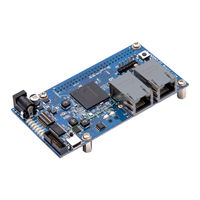
Renesas R-IN32M4-CL2 TESSERA User Manual (53 pages)
Gigabit Ethernet PHY Edition
Brand:
Renesas
| Category:
Network Hardware
| Size: 0.92 MB
Table of Contents
Table of Contents
6
1 Product Overview
11
Key Features
11
Superior PHY and Interface Technology
11
Best in Class Power Consumption
11
Key Specifications
11
Caution in this Manual<R
11
2 Functional Descriptions
12
Twisted Pair Media Interface
12
Voltage Mode Line Driver
12
Figure 2.1 Media Interface
12
Autonegotiation and Parallel Detection
13
Automatic Crossover and Polarity Detection
13
Table 2.1 Supported MDI Pair Combinations
13
Manual MDI/MDIX Setting
14
Link Speed Downshift
14
Actiphy Power Management
15
Figure 2.2 Actiphy State Diagram
15
Link Partner Wake-Up State
16
Low Power State
16
Normal Operating State
16
LED Interface
17
LED Modes
17
Table 2.2 LED Mode and Function Summary
17
LED Port Swapping
18
LED Behavior
18
Table 2.2 LED Mode and Function Summary
18
Fast Link Failure Indication
19
Testing Features
20
Ethernet Packet Generator
20
Far-End Loopback
21
Near-End Loopback
21
Figure 2.3 Far-End Loopback Diagram
21
Figure 2.4 Near-End Loopback Diagram
21
Connector Loopback
22
Figure 2.5 Connector Loopback Diagram
22
3 Registers
23
Figure 3.1 Register Space Diagram
23
Register and Bit Conventions
24
IEEE 802.3 and Main Registers
25
Table 3.1 IEEE 802.3 Registers
25
Table 3.2 Main Registers
25
Mode Control
26
Table 3.3 Mode Control, Address 0 (0X00)
26
Device Identification
27
Mode Status
27
Table 3.4 Mode Status, Address 1 (0X01)
27
Table 3.5 PHY Identifier 1, Address 2 (0X02)
27
Table 3.6 PHY Identifier 2, Address 3 (0X03)
27
Autonegotiation Advertisement
28
Link Partner Autonegotiation Capability
28
Table 3.7 Autonegotiation Advertisement, Address 4 (0X04)
28
Table 3.8 Autonegotiation Link Partner Ability, Address 5 (0X05)
28
Autonegotiation Expansion
29
Table 3.10 Autonegotiation Next Page Transmit, Address 7 (0X07)
29
Table 3.9 Autonegotiation Expansion, Address 6 (0X06)
29
Transmit Autonegotiation Next Page
29
1000BASE-T Control
30
Autonegotiation Link Partner Next
30
Table 3.11 Autonegotiation LP Next Page Receive, Address 8 (0X08)
30
Table 3.12 1000BASE-T Control, Address 9 (0X09)
30
1000BASE-T Status
31
1000BASE-T Status Extension 1
31
Table 3.13 1000BASE-T Status, Address 10 (0X0A)
31
Table 3.14 1000BASE-T Status Extension 1, Address 15 (0X0F)
31
1000BASE-T Status Extension 2
32
100BASE-TX Status Extension
32
Table 3.15 100BASE-TX Status Extension, Address 16 (0X10)
32
Table 3.16 1000BASE-T Status Extension 2, Address 17 (0X11)
32
Error Counter 1
33
Error Counter 2
33
Extended PHY Control 0
33
Table 3.16 1000BASE-T Status Extension 2, Address 17 (0X11)
33
Table 3.17 Extended PHY Control 0, Address 18 (0X12)
33
Table 3.18 Error Counter 1, Address 19 (0X13)
33
Table 3.19 Error Counter 2, Address 20 (0X14)
33
Error Counter 3
34
Extended Control and Status
34
Table 3.20 Error Counter 3, Address 21 (0X15)
34
Table 3.21 Extended Control and Status, Address 22 (0X16)
34
Extended PHY Control 1
35
Extended PHY Control 2
35
Table 3.22 Extended PHY Control 1, Address 23 (0X17)
35
Table 3.23 Extended PHY Control 2, Address 24 (0X18)
35
Interrupt Mask
36
Table 3.24 Interrupt Mask, Address 25 (0X19)
36
Interrupt Status
37
Table 3.25 Interrupt Status, Address 26 (0X1A)
37
Auxiliary Control and Status
38
Table 3.26 Auxiliary Control and Status, Address 28 (0X1C)
38
LED Behavior
39
LED Mode Select
39
Table 3.27 LED Mode Select, Address 29 (0X1D)
39
Table 3.28 LED Behavior, Address 30 (0X1E)
39
Extended
40
Table 3.28 LED Behavior, Address 30 (0X1E)
40
Table 3.29 Extended/General Purpose Register Page Access, Address 31 (0X1F)
40
Extended Page 1 Registers
41
Cu Media CRC Good Counter
41
Table 3.30 Extended Registers Page 1 Space
41
Table 3.31 Cu Media CRC Good Counter, Address 18E1 (0X12)
41
Extended Mode Control
42
Actiphy Control
42
Table 3.32 Extended Mode Control, Address 19E1 (0X13)
42
Table 3.33 Actiphy Control, Address 20E1 (0X14)
42
Table 3.33 Actiphy Control, Address 20E1 (0X14)
43
Ethernet Packet Generator Control 1
44
Table 3.34 EPG Control Register 1, Address 29E1 (0X1D)
44
Ethernet Packet Generator Control 2
45
Table 3.35 EPG Control Register 2, Address 30E1 (0X1E)
45
Extended Page 2 Registers
46
LED Control
46
Table 3.36 Extended Registers Page 2 Space
46
Table 3.37 LED Control, Address 17E2 (0X11)
46
General Purpose Registers
47
Reserved General Purpose Address Space
47
Reserved
47
Fast Link Failure Control
47
Enhanced LED Control
47
Table 3.38 Reserved, Address 14G (0X0E)
47
Table 3.39 Fast Link Failure Control, Address 19G (0X13)
47
Table 3.40 Enhanced LED Control, Address 25G (0X19)
47
Global Interrupt Status
48
Table 3.41 Global Interrupt Status, Address 29G (0X1D)
48
4 Design Considerations
49
Advertisement
Renesas R-IN32M4-CL2 TESSERA User Manual (98 pages)
CC-Link Remote device station
Brand:
Renesas
| Category:
Network Hardware
| Size: 1.76 MB
Table of Contents
Table of Contents
6
1 Introduction
11
Related Materials
11
Generic Terms and Abbreviations
11
CC-Link Partner Association
11
Cyclic Data Capacity
12
2 Function List
13
3 Specified Parts and Recommended Parts
14
Recommended Parts
14
4 R-IN32 Series Initialization
15
5 CC-Link Remote Device Station Pins
16
6 Setting Details
19
Setting the Number of Occupied Stations
19
Setting the Station Number and Baud Rate
20
Transmission Monitor Section Terminals (for LED)
21
7 Monitor Output of Reception Frame Information
23
8 Memory Map
24
Memory Map List
24
Memory Map Details
28
Send Data Write Enable Information (CCS_MWRENL_RCEX)
28
Station Number Switch Information, Number of Occupied Stations Information and Baud Rate Switch Information (CCS_M3STNO_BSW_KYOKU)
29
Error Information (CCS_M3ERR1_ERR2)
30
M → R Status Information (CCS_M3MRST1_ST2)
31
RY Reception Buffer (CCS_M3MRRY00_0F)
33
Rwwn Register (Ccs_M3Mrrwwn)
33
Send Data Write Complete Flag and Receive Data Read Request (CCS_M3SDOK_RDRQ)
34
Vendor Code (CCS_M3VENDORCODE)
35
Model Code and Version (CCS_M3MODELCODE_VERSION)
35
SDLED Illumination Time Setting and Timeout Time Setting (CCS_M3SDLED_TOVER)
36
Cyclic Communication (CCS_M3RMST1_ST2)
38
RX Update Buffer (Ccs_M3Rmrxn0_Nf)
39
Rwr Register (Ccs_M3Rmrwrn)
39
HOLD/CLR Register (CCS_M3HOLDCLR)
40
9 Sample Flowchart for CC-Link Version 1
41
Initial Setting
41
Main Processing
42
Synchronous Read Method / Asynchronous Write Method
42
Asynchronous Read Method / Asynchronous Write Method
44
Reception and Transmission Processing
45
Synchronous Read Method (Interrupt Processing)
45
Asynchronous Read Method
46
Asynchronous Write Method
47
Timeout Time Setting Change
48
Initial Setting Time → Normal Setting Time
48
Normal Setting Time → Initial Setting Time
49
10 Remote Device Station Common Specification
50
Cyclic Transmission Signals
50
Cyclic Transmission Signal Definitions
50
System Area Details
51
Remote Register
54
11 Overview of CC-Link Ver. 2
55
Characteristics of CC-Link Ver. 2
56
Extended Cyclic
56
Less Occupied Stations
57
Overview of Protocol
58
Overview of Extended Cyclic Communication
58
Transmission of Own Station Information
59
Extended Cyclic Header Information
61
Relationship between SQ Values and RX/RY, Rwr/Rww
65
12 Sample Flowchart for CC-Link Version 2
66
List of Modules and Variables
66
Initial Setting INT_CCV20
68
Transmission/Reception Processing
69
Example Using an Interrupt (CCS_REFSTB Signal)
69
Example of Polling
70
Transmission/Reception Processing Module (ICCV20)
71
Application Work Area Transfer Processing Module CHK20DONE
75
13 Notes on Developing with CC-Link Version 2
76
Hardware
76
Software (Firmware)
77
Write Timing at Transmission
78
Handling CC-Link Version 2 Work Area
80
14 Questions & Answers
81
Circuit Design in General
81
Software
83
Protocol and Others
91
Renesas R-IN32M4-CL2 TESSERA User Manual (82 pages)
Board design edition
Brand:
Renesas
| Category:
Computer Hardware
| Size: 1.29 MB
Table of Contents
Table of Contents
6
1 Overview
9
Definition of Pin Handling and Symbols in this Manual
9
2 Power/Reset Pins
10
Power-On/Off Sequence
10
Power Supply Pins
12
Reset Pins
13
3 Clock Input Pins
14
Pin Functions
14
Notes on Configuring the Oscillation Circuit
15
Configuration Example of Oscillation Circuits
17
4 PLL Power Supply Pins
18
Recommended Configuration of Filter
18
Notes on Placement of Peripheral Components
19
5 GPIO Port Pins
20
6 Gigabit Ethernet PHY Pins
21
Power Supply Peripheral Circuit
21
Circuit Configuration
21
Recommended Components
22
Peripheral Circuit of Pulse Transformer
23
Example of Circuit Configuration
23
Recommended Components
24
REF_REXT and REF_FILT Pins
25
Example of Circuit Configuration
25
Recommended Resistors
25
Recommended Ceramic Capacitors
25
PHYADD Pin Handling
26
Example of Pin Handling
26
Handling of Pins
26
Notes on Board Wiring
27
7 Thermal Design <R
30
Deciding on Whether Particular Measures for Heat Dissipation Are Required
30
Estimating Tj
30
Estimating Power Consumption
30
Thermal Resistances under the JEDEC Conditions (for Θja and Ψjt)
31
Results of Estimating Power Consumption of the 1-V Sub-Systems at Tj
32
Relation between Temperature Increases (∆T) and Thermal Resistance (Θja) at a Given Ambient
33
Temperature
33
Examples of Measures for Heat Dissipation
34
Measures for Heat Release in Designing the Board
35
Heat Dissipation from the Periphery (Including the Casing)
37
Caution <R
38
Handling of Unused Pins
38
8 CC-Link Pins
39
9 CC-Link IE Field Pins
41
Caution
41
10 External Mcu/Memory Interface Pins
42
External MCU Interface
43
Asynchronous-SRAM Supporting MCU Connection Mode
44
Synchronous-SRAM Supporting MCU Connection Mode
46
Synchronous-Burst-Transfer Supporting MCU Connection Mode
48
External Memory Interface
52
Asynchronous SRAM MEMC
52
Synchronous Burst Access MEMC
55
11 Serial Flash ROM Connection Pins
58
12 Asynchronous Serial Interface J Connection Pins
59
1 I 2 C Connection Pins
60
14 CAN Pins
61
15 CSIH Pins <R
62
One Master and One Slave
62
One Master and Two Slaves
62
16 A/D Converter Pins
63
17 Jtag/Trace Pins
64
18 Implementation Conditions
68
19 Package Information
69
20 Mount Pad Information
70
21 BSCAN Information
71
BSCAN Operating Conditions
71
Maximum Operating Frequency of TCK
71
Idcode
71
BSCAN Non-Supported Pins
72
How to Get BSDL
73
22 IBIS Information
74
23 Marking Information
75
24 Countermeasure for Noise <R
76
Stopping Clock Output
76
Advertisement
Renesas R-IN32M4-CL2 TESSERA Application Note (10 pages)
Driver/Middleware Set for Board
Brand:
Renesas
| Category:
Computer Hardware
| Size: 0.52 MB
Table of Contents
Table of Contents
1
Introduction
2
Package Contents
3
Folder Structure
4
Operating Environment
5
Website and Support
6
Advertisement
Related Products
Renesas R0E572860CFL00
Renesas REG10J0083-0100
Renesas RZ/A2M
Renesas RZ/A Series
Renesas R0E436640CPE00
Renesas R0E00030AKCT00
Renesas RL78/FGIC
Renesas RH850/D1x
Renesas R8C/1A
Renesas RS-485
Renesas Categories
Computer Hardware
Motherboard
Microcontrollers
Adapter
Switch
More Renesas Manuals
Login
Sign In
OR
Sign in with Facebook
Sign in with Google
Upload manual
Upload from disk
Upload from URL