Table of Contents
Advertisement
Advertisement
Table of Contents

Related Manuals for Xilinx SP701


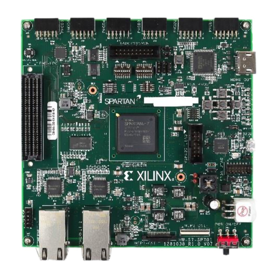
Summary of Contents for Xilinx SP701
- Page 1 SP701 Evaluation Board User Guide UG1319 (v1.0) July 12, 2019...
-
Page 2: Revision History
Revision History Revision History The following table shows the revision history for this document. Section Revision Summary 07/12/2019 Version 1.0 Initial release. UG1319 (v1.0) July 12, 2019 www.xilinx.com Send Feedback SP701 Board User Guide... -
Page 3: Table Of Contents
Chapter 3: Board Component Descriptions ........... 15 Overview.............................15 Component Descriptions......................15 Appendix A: VITA 57.1 FMC Connector Pinouts ..........44 Appendix B: Xilinx Design Constraints ............. 45 Overview.............................45 Appendix C: Regulatory and Compliance Information ......46 CE Information...........................46 Compliance Markings....................... 47 Appendix D: Additional Resources and Legal Notices ...... -
Page 4: Chapter 1: Introduction
Chapter 1 Introduction Overview The SP701 evaluation board is based on the XC7S100FGGA676 device, a member of the Xilinx ® 7 series FPGA family. It is optimized for low cost, low power, and high I/O performance. It comes with advanced high-performance FPGA logic based on real6-input look up table (LUT), 36 Kb... -
Page 5: Additional Resources
SP701 evaluation board. Block Diagram The following figure shows the various components of the SP701 Evaluation Board. Figure 1: SP701 Evaluation Board Block Diagram UG1319 (v1.0) July 12, 2019 www.xilinx.com... -
Page 6: Board Features
Chapter 1: Introduction Board Features The SP701 evaluation board features are listed here. Detailed information for each feature is provided in Chapter 3: Board Component Descriptions. • XC7S100-2FGGA676 package • Form factor: 6.00 in (152.4 mm) square, 0.08844 in (88.44 mils) thick •... -
Page 7: Board Specifications
• Width: 6.00 in (152.4 mm) • Thickness: 0.08844 in (88.44 mils) Note: A 3D model of this board is not available. See the SP701 board website documentation tab (Board Files check box) for the XDC listing and board schematics (0381874). Environmental •... - Page 8 Chapter 1: Introduction Operating Voltage • +12V UG1319 (v1.0) July 12, 2019 www.xilinx.com Send Feedback SP701 Board User Guide...
-
Page 9: Chapter 2: Board Setup And Configuration
® Product Support, place it back in its antistatic bag immediately. Board Components The following figure shows the SP701 board component locations. Each numbered component is keyed to the table in Board Component Location. IMPORTANT! The following figure is for visual reference only and might not reflect the current revision of the board. - Page 10 Chapter 2: Board Setup and Configuration Figure 2: SP701 Evaluation Board Components Round callout references a component Square callout references a component on the front side of the board on the back side of the board X22622-070119 UG1319 (v1.0) July 12, 2019 www.xilinx.com...
- Page 11 Omron B3U-1000P Power Input Connector, 2x6 (J30) Molex-39-30-1060 Power On/Off Slide Switch (SW11) C&K 1101M2S3AQE2 SP701 Board Power System, MPS (top and bottom) Monolithic Power Systems (MPS) 24-26 UG1319 (v1.0) July 12, 2019 www.xilinx.com Send Feedback SP701 Board User Guide...
-
Page 12: Default Switch And Jumper Settings
2-pin male header Power System Inhibit Jumper OFF Switches Default switch settings are listed in the following table. The table also references the respective schematic (0381874) page numbers. UG1319 (v1.0) July 12, 2019 www.xilinx.com Send Feedback SP701 Board User Guide... -
Page 13: Spartan-7 Device Configuration
Mode[001] SW13[1] = INIT_B, OFF = OPEN, ON = 0 = Spartan-7 Device Configuration The SP701 board supports two of the 7 series FPGA configuration modes: • Master SPI flash memory using the onboard QSPI flash memory • JTAG J5 micro-AB USB-JTAG interface connector ○... - Page 14 Configuration User Guide (UG470) for information on programming the SPI. 2. Set the boot mode pins SW13 [4:2] MODE[2:0] as indicated in the table in Spartan-7 Device Configuration for Master SPI. 3. Power-cycle the SP701 board. SW13 is callout 30 in Board Components. UG1319 (v1.0) July 12, 2019 www.xilinx.com...
-
Page 15: Chapter 3: Board Component Descriptions
[Figure 2, callout 1] A Spartan-7 XC7S100-2FGGA676C FPGA is installed on the SP701 evaluation board. The Spartan-7 family is optimized for low cost, lowest power, and high I/O performance. For further information on Spartan-7 FPGAs, see 7 Series FPGAs Data Sheet: Overview (DS180). - Page 16 Ethernet PHY 1/2 I/F, MIPI_CSI, I2C2_CAM VCCO_1V35 1.35V DDR3L I/F VADJ 1.8V (nom), LPC FMC I/F, MPS430_GPIO 3.3V, 2.5V VADJ 1.8V (nom), LPC FMC I/F, MPS430_GPIO 3.3V, 2.5V UG1319 (v1.0) July 12, 2019 www.xilinx.com Send Feedback SP701 Board User Guide...
- Page 17 This memory system is connected to FPGA U1 bank 34. The DDR3L 0.675V VTT termination voltage is supplied from MP20073DH regulator U13. The following figure shows the DDR3L memory interface. UG1319 (v1.0) July 12, 2019 www.xilinx.com Send Feedback SP701 Board User Guide...
- Page 18 Micron Technology website. The detailed FPGA connections for the feature described in this section are documented in the SP701 board XDC file, referenced in Appendix B: Xilinx Design Constraints. For more information, see the Zynq-7000 SoC and 7 Series Devices Memory Interface Solutions (UG586).
- Page 19 • U1 XCS700 FPGA • J21 FMC LPC connector • J3 2x7 2 mm shrouded, keyed JTAG pod flat cable connector The SP701 board JTAG chain is shown in the following figure. UG1319 (v1.0) July 12, 2019 www.xilinx.com Send Feedback...
- Page 20 Chapter 3: Board Component Descriptions Figure 6: SP701 JTAG Chain USB Conn FPGA_TMS_0 >TMS TMS> FPGA_TCK_0 TCK> >TCK FPGA_TDI_0 TDO> >TDI FPGA_TDO_0 <TDO TDI< FT4232H FPGA 7S100 JTAG Devices FMC_TMS_BUF >TMS VREF FMC_TCK_BUF >TCK SRST <PRSNT_L TMS> FMC_TDI_FPGA_TDO >TDI TCK>...
-
Page 21: Clock Generation
Chapter 3: Board Component Descriptions Clock Generation The SP701 board provides an I2C programmable (10 MHz – 810 MHz) Si570 oscillator (U45) to source the 200 MHz default SYSCLK. The U45 (I2C address 0x5D) I2C02_SYSOSC bus is connected to U23 TCA9548A main I2C0 bus switch channel 1. The U45 Si570 LVDS output is connected to FPGA U1 bank 33 MRCC pins AE8 (P) and AE7 (N). - Page 22 USB UART Interface [Figure 2, callout 13] The FT4232HQ U6 multifunction USB-UART on the SP701 board provides two level-shifted UART connections through the single micro-AB USB connector J5. • Channel ADBUS is configured in JTAG mode to support the JTAG chain •...
- Page 23 The FTDI FT4232HQ data sheet is available on the Future Technology Devices International Ltd. website. The detailed FPGA connections for the feature described in this section are documented in the SP701 board XDC file, referenced in Appendix B: Xilinx Design Constraints.
- Page 24 Crystal X22792-050319 The SP701 evaluation board uses dual TI PHY device DP83867IRPAP (U14, U16) for Ethernet communications at 10 Mb/s, 100 Mb/s, or 1000 Mb/s. The board only supports the RGMII mode. Each PHY connects to a user-provided Ethernet cable through RJ-45 connector (J9, J11), Wurth 7499111221A with built-in magnetics, and status LEDs.
- Page 25 Chapter 3: Board Component Descriptions Figure 10: Ethernet JTAG X22793-042619 The detailed FPGA connections for the feature described in this section are documented in the SP701 board XDC file, referenced in Appendix B: Xilinx Design Constraints. Ethernet PHY Status LEDs...
- Page 26 [Figure 2, callout 17] The SP701 evaluation board I2C bus implementation consists of bus I2C0, shared by the FPGA U1 HP bank 16 and the MSP430 system controller U25. The I2C bus is routed to a TCA9548A 1- to-8 bus switch U23 (address 0x74). Seven of the eight bus switch channels are used. The bus switch can operate at speeds up to 400 kHz.
- Page 27 VSEL0_VADJ Q17 FB_VADJ_VSEL0 U40 MP8756G VADJ regulator feedback adjusting switch VSEL1_VADJ Q18 FB_VADJ_VSEL1 U40 MP8756G VADJ regulator feedback adjusting switch 12VCURSNS_ALERT U32 INA226 POWER MONITOR ON INPUT 12V UG1319 (v1.0) July 12, 2019 www.xilinx.com Send Feedback SP701 Board User Guide...
- Page 28 The TI TCA9548 and TCA6416 data sheets are on the Texas Instruments website. The detailed FPGA connections for the feature described in this section are documented in the SP701 board XDC file, referenced in Appendix B: Xilinx Design Constraints HDMI Video Output...
- Page 29 For more details, see the ADV7511KSTZ-P data sheet at the Analog Devices website. The detailed FPGA connections for the feature described in this section are documented in the SP701 board XDC file, referenced in Appendix B: Xilinx Design Constraints. MIPI-CSI and MIPI-DSI...
- Page 30 Appendix B: Xilinx Design Constraints. MIPI-CSI The SP701 board supports MIPI-CSI. The Digilent PCAM module has been tested with this board. MIPI-CSI interface is connected to AMP/TE Connectivity 1-1734248-5 15-pin connector J8. MIPI-CSI interface is shown in the following figure.
- Page 31 Chapter 3: Board Component Descriptions MIPI-DSI The SP701 board provides MIPI DSI (display serial interface) support. The MIPI-DSI interface is connected to Hirose FH34SJ-34S-0.5SH 34-pin connector J20. The MIPI-DSI interface is shown in the following figure. Figure 15: MIPI-DSI Interface...
- Page 32 Chapter 3: Board Component Descriptions Power and Status LEDs [Figure 2, callout 20] The following table lists the SP701 power, user, and status LEDs. Table 11: SP701 Power, User, and Status LEDs Reference Designator Description (Green Unless Otherwise Noted) DONE (blue)
- Page 33 [Figure 2, callout 20, 21] The SP701 evaluation board implements six right-angle PMOD GPIO receptacles J14-J19. The 3.3V PMOD nets are wired to the XC7S100 FPGA 3.3V bank 16. For more information about PMOD connector compatible PMOD modules, see the Digilent Inc.
- Page 34 GPIO x8 3.3V GPIO x8 X22799-050319 The detailed FPGA connections for the feature described in this section are documented in the SP701 board XDC file, referenced in Appendix B: Xilinx Design Constraints. UG1319 (v1.0) July 12, 2019 www.xilinx.com Send Feedback...
- Page 35 TCA9548 X22800-051019 A host PC resident system controller user interface (SCUI) is provided on the SP701 website. This GUI enables you to query and control select programmable features such as clocks, FMC functionality, and power systems parameters. The SP701 documentation also includes a tutorial on the SCUI, SP701 System Controller Tutorial (XTP551), and a SP701 Software Install and Board Setup Tutorial (XTP552).
- Page 36 160 pins. The connector is keyed so that a mezzanine card, when installed in the FMC LPC connector on the SP701 evaluation board, faces away from the board. The FMC LPC connector pinout is shown in the Appendix A: VITA 57.1 FMC Connector...
- Page 37 CAUTION! Do NOT plug a PC ATX power supply 6-pin connector into the SP701 board power connector J30. The ATX 6-pin connector has a different pin-out than J30. Connecting an ATX 6-pin connector into J30 damages the SP701 board and voids the board warranty.
- Page 38 [Figure 2, callout 29] The SP701 power system is comprised of monolithic power systems components. The four outputs (VCCINT, VCCO_1V8, VCCO_2V5, and VCCO_3V3) of the MP5470 U34 regulator are adjustable through its I2C bus connection accessible from the FPGA U1 Bank 16 and the MSP430 system controller.
- Page 39 3.3V AUX for FMC 2A Buck MPM3805 1.1V 2x DP83867IR Core Input: 2.5V-6B (2x 125mA) 0.6A Buck X22801-050319 The following table lists the SP701 power system voltage regulators. Table 12: SP701 Power System Power Ref. Power Rail Max. Schematic Device Type Description Rail Des.
- Page 40 POL switching VADJ 1.80V regulator MP20073DH DDR memory VTTREF VTTREF 0.675V termination regulator The following figure shows the SP701 power system sequencing diagram. Figure 22: Power System Sequence POWER UP SEQUENCE SYS CTRL 3V3AUX MSP430 VCCINT_1V VCCO_1V8 VCCO_2V5 VCCO_3V3 VCCO_1V35...
- Page 41 Xilinx device and the various other on-board supplies. The analog mixed signal (AMS) block present in Xilinx 7 series FPGAs is called XADC (includes SYSMON function). Apart from the SYSMON function, the ADCs provide a general-purpose, high-precision analog interface for a range of applications.
- Page 42 The following figure shows the SYSMON implementation and SYSMON header J24, a 2x10 shrouded male pin header. Jumper J26 is provided to select internal reference or external reference. UG1319 (v1.0) July 12, 2019 www.xilinx.com Send Feedback SP701 Board User Guide...
- Page 43 Chapter 3: Board Component Descriptions Figure 24: XADC (SYSMON) Interface X22606-040219 See the SP701 schematic 0381874 for detailed SYSMON header J24 and XADC_VREF option details. UG1319 (v1.0) July 12, 2019 www.xilinx.com Send Feedback SP701 Board User Guide...
-
Page 44: Appendix A: Vita 57.1 Fmc Connector Pinouts
VITA 57.1 FMC Connector Pinouts The following figure shows the pinout of the FPGA mezzanine card (FMC) low pin count (LPC) connector defined by the VITA 57.1 FMC specification. For a description of how the SP701 evaluation board implements the FMC specification, see... -
Page 45: Appendix B: Xilinx Design Constraints
The Xilinx design constraints (XDC) file template for the SP701 board provides for designs targeting the SP701 evaluation board. Net names in the constraints file correlate with net names on the latest SP701 evaluation board schematic. Identify the appropriate pins and replace the net names with net names in the user RTL. -
Page 46: Appendix C: Regulatory And Compliance Information
CE Safety IEC 60950-1:2005, Information technology equipment – Safety, Part 1: General requirements EN 60950-1:2006, Information technology equipment – Safety, Part 1: General requirements UG1319 (v1.0) July 12, 2019 www.xilinx.com Send Feedback SP701 Board User Guide... -
Page 47: Compliance Markings
Xilinx has met its national obligations to the EU WEEE Directive by registering in those countries to which Xilinx is an importer. Xilinx has also elected to join WEEE Compliance Schemes in some countries to help manage customer returns at end-of-life. -
Page 48: Appendix D: Additional Resources And Legal Notices
• On Windows, select Start → All Programs → Xilinx Design Tools → DocNav. • At the Linux command prompt, enter docnav. Xilinx Design Hubs provide links to documentation organized by design tasks and other topics, which you can use to learn key concepts and address frequently asked questions. To access the Design Hubs: •... -
Page 49: References
Appendix D: Additional Resources and Legal Notices References The most up to date information related to the SP701 board and its documentation is available on the following websites. • SP701 Evaluation Kit • SP701 Evaluation Kit Master Answer Record 72092 These documents provide supplemental material useful with this guide: 1. -
Page 50: Please Read: Important Legal Notices
IP cores may be subject to warranty and support terms contained in a license issued to you by Xilinx. Xilinx products are not designed or intended to be fail-safe or for use in any application requiring fail-safe performance; you assume sole risk and liability for...
Need help?
Do you have a question about the SP701 and is the answer not in the manual?
Questions and answers