Xilinx SP605 Hardware User's Manual
Hide thumbs
Also See for SP605:
- User manual (67 pages) ,
- Hardware setup manual (2 pages) ,
- Hardware tutorial (40 pages)
Table of Contents
Advertisement
Quick Links
Advertisement
Table of Contents

Related Manuals for Xilinx SP605


Summary of Contents for Xilinx SP605
- Page 1 SP605 Hardware User Guide UG526 (v1.9) February 14, 2019...
-
Page 2: Revision History
(including loss of data, profits, goodwill, or any type of loss or damage suffered as a result of any action brought by a third party) even if such damage or loss was reasonably foreseeable or Xilinx had been advised of the possibility of the same. - Page 3 Regulatory and Compliance Information. 02/14/19 Updated the Electrostatic Discharge Caution section, Appendix C, Xilinx Design Constraints, and Appendix D, Regulatory and Compliance Information. Updated 2. 128 MB DDR3 Component Memory. UG526 (v1.9) February 14, 2019 www.xilinx.com SP605 Hardware User Guide...
- Page 4 SP605 Hardware User Guide www.xilinx.com UG526 (v1.9) February 14, 2019...
-
Page 5: Table Of Contents
..........8 Chapter 1: SP605 Evaluation Board Overview . - Page 6 Appendix A: Default Jumper and Switch Settings Appendix B: VITA 57.1 FMC LPC Connector Pinout Appendix C: Xilinx Design Constraints Overview ..............65...
-
Page 7: Preface: About This Guide
Preface About This Guide This manual accompanies the Spartan®-6 FPGA SP605 Evaluation Board and contains information about the SP605 hardware and software tools. Guide Contents This manual contains the following chapters: • Chapter 1, SP605 Evaluation Board, provides an overview of and details about the components and features of the SP605 board. -
Page 8: Additional Support Resources
PCB and interface level. Additional Support Resources To search the database of silicon and software questions and answers or to create a technical support request in the Request Portal, see the Xilinx website. www.xilinx.com SP605 Hardware User Guide UG526 (v1.9) February 14, 2019... -
Page 9: Chapter 1: Sp605 Evaluation Board
Chapter 1 SP605 Evaluation Board Overview The SP605 board enables hardware and software developers to create or evaluate designs targeting the Spartan®-6 XC6SLX45T-3FGG484 FPGA. The SP605 provides board features common to many embedded processing systems. Some commonly used features include: a DDR3 component memory, a 1-lane PCI Express®... -
Page 10: Features
Chapter 1: SP605 Evaluation Board Features The SP605 board provides the following features (see Figure 1-2 Table 1-1): • 1. Spartan-6 XC6SLX45T-3FGG484 FPGA • 2. 128 MB DDR3 Component Memory • 3. SPI x4 Flash • 4. Linear BPI Flash •... -
Page 11: Block Diagram
5. System ACE CF and CompactFlash Connector • 6. USB JTAG Block Diagram The following figure shows a high-level block diagram of the SP605 and its peripherals. X-Ref Target - Figure 1-1 1-Lane I/Fs: PCIe 125 MHz Clk Part of PCIe Edge Conn. -
Page 12: Related Xilinx Documents
Put the adapter down only on an anti-static surface such as the bag supplied in your kit. • If you are returning the adapter to Xilinx Product Support, place it back in its anti- static bag immediately. www.xilinx.com SP605 Hardware User Guide... -
Page 13: Detailed Description
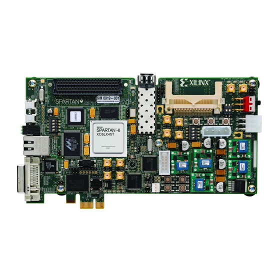
X-Ref Target - Figure 1-2 15b 15a 16a 15f 3, 14 (on back side) UG526_02 _092412 Figure 1-2: SP605 Board The numbered features in Figure 1-2 correlate to the features and notes listed in Table 1-1. - Page 14 Chapter 1: SP605 Evaluation Board Table 1-1: SP605 Features (Cont’d) Schematic Number Feature Notes Page 200 MHz OSC, oscillator socket, Clock Generation 13, 14 SMA connectors a. 200 MHz oscillator SiTime 200 MHz 2.5V LVDS b. Oscillator socket, single- MMD Components 2.5V 27 MHz ended, LVCMOS c.
-
Page 15: Spartan-6 Xc6Slx45T-3Fgg484 Fpga
Mini-Fit Type 6-Pin, ATX 12V input power connectors Type 4-pin 1. Spartan-6 XC6SLX45T-3FGG484 FPGA A Xilinx Spartan-6 XC6SLX45T-3FGG484 FPGA is installed on the SP605 Evaluation Board. See the Spartan-6 FPGA Data Sheet (DS162). [Ref 1] Configuration The SP605 supports configuration in the following modes: •... -
Page 16: I/O Voltage Rails
2. 128 MB DDR3 Component Memory The SP605 128 MB 16-bit wide DDR3 memory consists of a single 1 Gb x 16 SDRAM U42 wired to Bank 3 (V = 1.5V) of the U1 XC6SLX45T FPGA. The Spartan-6 FPGA hard memory controller is used for data transfer across the DDR3 memory interface’s 16-bit... - Page 17 U1 FPGA Schematic Net Name Pin Number Pin Name MEM1_A0 MEM1_A1 MEM1_A2 MEM1_A3 MEM1_A4 MEM1_A5 MEM1_A6 MEM1_A7 MEM1_A8 MEM1_A9 MEM1_A10 A10/AP MEM1_A11 MEM1_A12 A12/BCN MEM1_A13 NC/A13 MEM1_A14 NC/A14 MEM1_BA0 MEM1_BA1 MEM1_BA2 SP605 Hardware User Guide www.xilinx.com UG526 (v1.9) February 14, 2019...
- Page 18 MEM1_DQ13 DQ10 MEM1_DQ14 DQ14 MEM1_DQ15 DQ12 MEM1_WE_B WE_B MEM1_RAS_B RAS_B MEM1_CAS_B CAS_B MEM1_ODT MEM1_CLK_P CLK_P MEM1_CLK_N CLK_N MEM1_CKE MEM1_LDQS_P LDQS_P MEM1_LDQS_N LDQS_N MEM1_UDQS_P UDQS_P MEM1_UDQS_N UDQS_N MEM1_LDM MEM1_UDM MEM1_RESET_B RESET_B www.xilinx.com SP605 Hardware User Guide UG526 (v1.9) February 14, 2019...
-
Page 19: Spi X4 Flash
[Ref 3] 3. SPI x4 Flash The Xilinx Spartan-6 FPGA hosts a SPI interface which is visible to the Xilinx iMPACT configuration tool. The SPI memory device operates at 3.0V; the Spartan-6 FPGA I/Os are 3.3V tolerant and provide electrically compatible logic levels to directly access the SPI flash through a 2.5V bank. - Page 20 1. Not a U1 FPGA pin See the Winbond Serial Flash Memory Data Sheet for more information. [Ref 16] See the XPS Serial Peripheral Interface Data Sheet (DS570) for more information. [Ref 4] www.xilinx.com SP605 Hardware User Guide UG526 (v1.9) February 14, 2019...
-
Page 21: Linear Bpi Flash
Detailed Description 4. Linear BPI Flash A Numonyx JS28F256P30 Linear Flash memory (U25) on the SP605 (Figure 1-5) provides 32 MB of non-volatile storage that can be used for configuration as well as software storage. The Linear Flash is operated in asynchronous mode. - Page 22 FLASH_D9 AB19 FLASH_D10 DQ10 AA18 FLASH_D11 DQ11 AB18 FLASH_D12 DQ12 FLASH_D13 DQ13 AA12 FLASH_D14 DQ14 AB12 FLASH_D15 DQ15 FMC_PWR_GOOD_FLASH_RST_B RST_B FLASH_WE_B WE_B FLASH_OE_B OE_B FLASH_CE_B CE_B FLASH_ADV_B ADV_B FLASH_WAIT WAIT www.xilinx.com SP605 Hardware User Guide UG526 (v1.9) February 14, 2019...
-
Page 23: Fpga Design Considerations For The Configuration Flash
Detailed Description FPGA Design Considerations for the Configuration Flash The SP605 has the P30 BPI flash connected to the FPGA dual use configuration pins and is not shared. It can be used to configure the FPGA, and then controlled post-configuration via the FPGA fabric. - Page 24 SYSACE_D0 MPD00 SYSACE_D1 MPD01 SYSACE_D2 MPD02 SYSACE_D3 MPD03 SYSACE_D4 MPD04 SYSACE_D5 MPD05 SYSACE_D6 MPD06 SYSACE_D7 MPD07 SYSACE_MPA00 MPA00 SYSACE_MPA01 MPA01 SYSACE_MPA02 MPA02 SYSACE_MPA03 MPA03 SYSACE_MPA04 MPA04 SYSACE_MPA05 MPA05 SYSACE_MPA06 MPA06 www.xilinx.com SP605 Hardware User Guide UG526 (v1.9) February 14, 2019...
-
Page 25: Usb Jtag
6. USB JTAG JTAG configuration is provided through onboard USB-to-JTAG configuration logic where a computer host accesses the SP605 JTAG chain through a Type-A (computer host side) to Type-Mini-B (SP605 side) USB cable. The JTAG chain of the board is illustrated in Figure 1-6. -
Page 26: Clock Generation
1-7. When the VITA 57.1 FMC LPC expansion connector is populated with an expansion module that has a JTAG chain, jumper J19 must be set to connect pins 2-3 in order to include the FMC expansion module's JTAG chain in the main SP605 JTAG chain. -
Page 27: Oscillator Socket (Single-Ended, 2.5V Or 3.3V)
Oscillator Socket (Single-Ended, 2.5V or 3.3V) One populated single-ended clock socket (X2) is provided for user applications. The option of 2.5V or 3.3V power may be selected via a 0Ω resistor selection. The SP605 board is shipped with a 27 MHz 2.5V oscillator installed. -
Page 28: Sma Connectors (Differential)
One (1) MGT is wired to MGT SMA connectors (J36, J37) • One (1) MGT is wired to the SFP Module connector (P2) The SP605 includes a set of six SMA connectors for the GTP (MGT) RX/TX Port and GTP (MGT) Clock as described in Figure 1-10 Table 1-10. - Page 29 32K10K-400E3 GND1 MGT REFCLK GND2 GND3 SMA_REFCLK_C_N GND4 GND5 GND6 GND7 SMA_REFCLK_N SMA_REFCLK_P J37 32K10K-400E3 GND1 GND2 GND3 SMA_REFCLK_C_P GND4 GND5 GND6 GND7 UG526_10 _092409 Figure 1-10: GTP SMA Clock SP605 Hardware User Guide www.xilinx.com UG526 (v1.9) February 14, 2019...
- Page 30 Chapter 1: SP605 Evaluation Board Table 1-10: GTP SMA Clock Connections U1 FPGA Pin Schematic Net Name SMA Pin SMA_RX_N J35.1 SMA_RX_P J34.1 SMA_TX_N J33.1 SMA_TX_P J32.1 SMA_REFCLK_N J36.1 SMA_REFCLK_P J37.1 www.xilinx.com SP605 Hardware User Guide UG526 (v1.9) February 14, 2019...
-
Page 31: Pci Express Endpoint Connectivity
AC adapter might be required. If a different AC adapter is used, its load regulation should be better than ±10%. SP605 power slide switch SW2 turns the board on and off by controlling the 12V supply to the board. - Page 32 Chapter 1: SP605 Evaluation Board SP605 board. The 6-pin Mini-Fit type connector is marked with a no PCIe power label to warn users of the potential hazard. See the Spartan-6 FPGA GTP Transceivers User Guide (UG386) for more information. [Ref 6]...
-
Page 33: Sfp Module Connector
Pin Name SFP_RX_P SFP_RX_N SFP_TX_P SFP_TX_N SFP_LOS SFP_TX_DISABLE_FPGA TX_DISABLE SFPCLK_QO_N U47.6 SFPCLK_QO_P U47.7 Notes: 1. The 125MHz SFP clock is sourced by clock driver U47. 2. Not P2 SFP module pins. SP605 Hardware User Guide www.xilinx.com UG526 (v1.9) February 14, 2019... -
Page 34: 100/1000 Tri-Speed Ethernet Phy
SP605 Evaluation Board 11. 10/100/1000 Tri-Speed Ethernet PHY The SP605 uses the onboard Marvell Alaska PHY device (88E1111) for Ethernet communications at 10, 100, or 1000 Mb/s. The board supports a GMII interface from the FPGA to the PHY. The PHY connection to a user-provided Ethernet cable is through a Halo HFJ11-1G01E RJ-45 connector with built-in magnetics. - Page 35 PHY_TXD6 TXD6 PHY_TXD7 TXD7 See the Marvell Alaska Gigabit Ethernet Transceivers product page [Ref 20] and the LogiCORE™ IP Tri-Mode Ethernet MAC User Guide (UG138) [Ref 7] for more information. SP605 Hardware User Guide www.xilinx.com UG526 (v1.9) February 14, 2019...
-
Page 36: Usb-To-Uart Bridge
The SP605 contains a Silicon Labs CP2103GM USB-to-UART bridge device (U4) which allows connection to a host computer with a USB cable. The USB cable is supplied in this evaluation kit (Type A end to host computer, Type Mini-B end to SP605 connector J23). Table 1-16 details the SP605 J23 pinout. -
Page 37: Dvi Codec
Pin Number Pin Name DVI_D0 DVI_D1 DVI_D2 DVI_D3 DVI_D4 DVI_D5 DVI_D6 DVI_D7 DVI_D8 DVI_D9 DVI_D10 DVI_D11 DVI_DE DVI_H DVI_RESET_B RESET_B DVI_V DVI_XCLK_N XCLK_N DVI_XCLK_P XCLK_P No Connect DVI_GPIO0 GPIO0 DVI_GPIO1 GPIO1 SP605 Hardware User Guide www.xilinx.com UG526 (v1.9) February 14, 2019... -
Page 38: Iic Bus
Chapter 1: SP605 Evaluation Board 14. IIC Bus The SP605 implements three IIC bus interfaces at the FPGA. The MAIN IIC bus hosts four items: • FPGA U1 Bank 1 “MAIN” IIC interface • 8-Kb NV Memory U4 • FMC LPC connector J2 •... -
Page 39: Iic External Access Header
J45 (see Figure 1-12) is a two-pin header that allows external IIC devices to be connected to the SP605 IIC bus. When connected, the external device can be accessed via IIC commands using IIC_SDA_MAIN and IIC_SCL_MAIN. 8-Kb NV Memory The SP605 hosts a 8-Kb ST Microelectronics M24C08-WDW6TP IIC parameter storage memory device (U4). - Page 40 Not Applicable Tied to GND See the ST Micro M24C08 Data Sheet for more information. [Ref 21] In addition, see the Xilinx XPS IIC Bus Interface Data Sheet (DS606). [Ref 8] www.xilinx.com SP605 Hardware User Guide UG526 (v1.9) February 14, 2019...
-
Page 41: Status Leds
DDR3 PWR GD DDR3 1.5V Power On DS17 FPGA_INIT_B INIT FPGA INIT System ACE CF DS18 SYSACE_ERR_LED System ACE CF Error Error LED DS19 MGT_POWERGOOD Green MGT_AVCC GD MGT_AVCC Power On SP605 Hardware User Guide www.xilinx.com UG526 (v1.9) February 14, 2019... -
Page 42: Ethernet Phy Status Leds
The Ethernet PHY status LEDs (DS11-DS13) are mounted in right-angle plastic housings to make them visible on the connector end of the board when the SP605 board is installed into a PC motherboard. This cluster of six LEDs is installed adjacent to the RJ45 Ethernet jack... -
Page 43: Fpga Init And Done Leds
Detailed Description FPGA INIT and DONE LEDs The typical Xilinx FPGA power up and configuration status LEDs are present on the SP605. The red INIT LED DS17 comes on momentarily after the FPGA powers up and during its internal power-on process. The DONE LED DS2 comes on after the FPGA programming bitstream has been downloaded and the FPGA successfully configured. -
Page 44: User I/O
Chapter 1: SP605 Evaluation Board 16. User I/O The SP605 provides the following user and general purpose I/O capabilities: • User LEDs • User Pushbutton Switches • User DIP Switch • User SIP Header • User SMA GPIO User LEDs... -
Page 45: User Pushbutton Switches
Detailed Description User Pushbutton Switches The SP605 provides five active-High pushbutton switches: SW4, SW5, SW6, SW7, and SW8. The five pushbuttons all have the same topology as the sample shown in Figure 1-16. Four pushbuttons are assigned as GPIO, and the fifth is assigned as a CPU_RESET. -
Page 46: User Dip Switch
Chapter 1: SP605 Evaluation Board User DIP Switch The SP605 includes an active-High four-pole DIP switch, as described in Figure 1-17 Table 1-25. Three poles (switches 1-3) are pulled up to 2.5V, and one pole (switch 4) is pulled up to 1.5V, when closed. -
Page 47: User Sip Header
Detailed Description User SIP Header The SP605 includes a 6-pin single-inline (SIP) male pin header (J55) for FPGA GPIO access. Four pins of J55 are wired to the FPGA through 200Ω series resistors and a level shifter, and the remaining two J55 pins are wired to 3.3V and GND. The J55 header is described in... -
Page 48: User Sma Gpio
Chapter 1: SP605 Evaluation Board User SMA GPIO The SP605 includes an pair of SMA connectors for GPIO as described in Figure 1-19 Table 1-27. X-Ref Target - Figure 1-19 32K10K-400E3 GND1 GND2 GND3 GND4 GND5 GND6 GND7 USER_SMA_GPIO_N 32K10K-400E3... -
Page 49: Switches
Mode DIP Switch SW1 (Active-High) Power On/Off Slide Switch SW2 SW2 is the SP605 board main power on/off switch. Sliding the switch actuator from the off to on position applies 12V power from either J18 (6-pin Mini-Fit) or J27 (4-pin ATX) power connector to the VCC12_P power plane. -
Page 50: Fpga_Prog_B Pushbutton Sw3 (Active-Low)
5. System ACE CF and CompactFlash Connector for more details. X-Ref Target - Figure 1-22 Silkscreen: "SYSACE RESET" SYSACE_RESET_B Pushbutton UG526_22 _092409 Figure 1-22: System ACE CF RESET_B Pushbutton SW9 www.xilinx.com SP605 Hardware User Guide UG526 (v1.9) February 14, 2019... -
Page 51: System Ace Cf Compactflash Image Select Dip Switch S1 (Active-High)
5. System ACE CF and CompactFlash Connector for more details. X-Ref Target - Figure 1-23 VCC2V5 SYSACE_CFGMODEPIN SYSACE_CFGADDR2 SYSACE_CFGADDR1 SYSACE_CFGADDR0 SDMX-4-X UG526_23 _102709 Figure 1-23: System ACE CF CompactFlash Image Select DIP Switch S1 SP605 Hardware User Guide www.xilinx.com UG526 (v1.9) February 14, 2019... -
Page 52: Mode Dip Switch Sw1 (Active-High)
UG526_24 _092409 Figure 1-24: FPGA Mode DIP Switch SW1 For more information, refer to the Spartan-6 FPGA Configuration User Guide (UG380) [Ref 2]. See Table 1-32 for the configuration modes. www.xilinx.com SP605 Hardware User Guide UG526 (v1.9) February 14, 2019... -
Page 53: Vita 57.1 Fmc Lpc Connector
2 differential clocks Note: The SP605 board VADJ voltage for the FMC LPC connector J2 is fixed at 2.5V (non- adjustable). The 2.5V rail cannot be turned off. The SP605 VITA 57.1 FMC interfaces are compatible with 2.5V mezzanine cards capable of supporting 2.5V VADJ. - Page 54 AB10 FMC_LA23_N IIC_SCL_MAIN FMC_LA26_P IIC_SDA_MAIN FMC_LA26_N FMC_CLK1_M2C_P FMC_PRSNT_M2C_L FMC_CLK1_M2C_N FMC_CLK0_M2C_P FMC_LA00_CC_P FMC_CLK0_M2C_N FMC_LA00_CC_N FMC_LA02_P FMC_LA03_P FMC_LA02_N FMC_LA03_N FMC_LA04_P FMC_LA08_P FMC_LA04_N FMC_LA08_N FMC_LA07_P FMC_LA12_P FMC_LA07_N FMC_LA12_N FMC_LA11_P FMC_LA16_P FMC_LA11_N FMC_LA16_N FMC_LA15_P www.xilinx.com SP605 Hardware User Guide UG526 (v1.9) February 14, 2019...
-
Page 55: Power Management
Mini-Fit type connector J18. The AC-to-DC power supply included in the kit has a mating 6-pin plug. When the SP605 is installed into a table top or tower PC's PCIe slot, the SP605 is typically powered from the PC ATX power supply. One of the PC’s ATX hard disk type 4-pin power connectors is plugged into SP605 connector J27. - Page 56 J27 at the same time as this will damage the SP605 board. Refer to Figure 1-20 for details. The SP605 Power can be turned on or off through the board mounted slide switch SW2. When the switch is in the on position, a green LED (DS14) is illuminated.
-
Page 57: Onboard Power Regulation
Detailed Description Onboard Power Regulation The following figure shows the SP605 onboard power supply architecture. The SP605 uses Texas Instruments power controllers for primary core power control and monitoring. X-Ref Target - Figure 1-25 Power Supply Jack J18 or J27... - Page 58 (Addr 52) _FPGA down down down Rail VCCAUX 2.375 Rail VCC1V5 1.425 1.38 1.68 _FPGA UCD9240 Shut Shut Shut 13.203 (Addr 53) down down down Rail VCC3V3 3.135 3.036 3.696 www.xilinx.com SP605 Hardware User Guide UG526 (v1.9) February 14, 2019...
- Page 59 UCD92xx series of controllers from a Windows- based host computer via the PMBus pod. The SP605 onboard connector J1 is wired for the TI EVM interface and provides access to the PMBUS and UCD9240s for monitoring purposes.
-
Page 60: Configuration Options
4. Default setting due to internal pull-up termination on Mode pins. With the mode switch SW1 set to 01, the SP605 will attempt to boot or load a bitstream from either the SPI X4 Flash device U32 or a user supplied SPI Flash memory mezzanine... - Page 61 Appendix A Default Jumper and Switch Settings Table A-33 shows the default switch settings and Table A-34 shows the default jumper settings for the SP605. Table A-33: Default Switch Settings REFDES Function/Type Default Board power slide-switch FPGA mode 2-pole DIP switch, Slave SelectMAP...
-
Page 62: Appendix A: Default Jumper And Switch Settings
Jump 1-2 SFP Enabled Jump 1-2 SPI Memory Select SPI Select SPI X4 Memory U32 Jump 1-2 System ACE CF Error LED System ACE CF Error LED DS18 Enabled Jump 1-2 www.xilinx.com SP605 Hardware User Guide UG526 (v1.9) February 14, 2019... -
Page 63: Appendix B: Vita 57.1 Fmc Lpc Connector Pinout
G ND VADJ 3P3V V ADJ G ND 3P 3V UG526_26_092709 Figure B-26: FMC LPC Connector Pinout For more information, refer to the VITA 57.1 FMC LPC Connections table (Table 1-28). SP605 Hardware User Guide www.xilinx.com UG526 (v1.9) February 14, 2019... - Page 64 Appendix B: VITA 57.1 FMC LPC Connector Pinout www.xilinx.com SP605 Hardware User Guide UG526 (v1.9) February 14, 2019...
-
Page 65: Appendix C: Xilinx Design Constraints
The Xilinx Design Constraints (XDC) file template provides for designs targeting the SP605 evaluation board. Net names in the constraints correlate with net names on the latest SP605 evaluation board schematic. Identify the appropriate pins and replace the net names with net names in the user RTL. - Page 66 Appendix C: Xilinx Design Constraints www.xilinx.com SP605 Hardware User Guide UG526 (v1.9) February 14, 2019...
-
Page 67: Appendix D: Regulatory And Compliance Information
Information This product is designed and tested to conform to the European Union directives and standards described in this section. See the Spartan-6 FPGA SP605 - Known Issues and Release Notes Xilinx Master Answer Record 33839 concerning the CE requirements for the PC Test Environment. -
Page 68: Markings
Xilinx has met its national obligations to the EU WEEE Directive by registering in those countries to which Xilinx is an importer. Xilinx has also elected to join WEEE Compliance Schemes in some countries to help manage customer returns at end-of-life. - Page 69 This appendix provides references to documentation supporting Spartan-6 FPGAs, tools, and IP. For additional information, see www.xilinx.com/support/documentation/index.htm. Spartan-6 FPGA SP605 - Known Issues and Release Notes Xilinx Master Answer Record 33839 Xilinx documents supporting the SP605 Evaluation Board: DS162, Spartan-6 FPGA Data Sheet: DC and Switching Characteristics...
- Page 70 Appendix E: References www.xilinx.com SP605 Hardware User Guide UG526 (v1.9) February 14, 2019...
Need help?
Do you have a question about the SP605 and is the answer not in the manual?
Questions and answers