Table of Contents
Advertisement
Quick Links
Advertisement
Table of Contents

Subscribe to Our Youtube Channel
Related Manuals for Alinx AX7Z035B


Summary of Contents for Alinx AX7Z035B
- Page 1 ZYNQ7000 FPGA Development Board AX7Z035B User Manual...
-
Page 2: Table Of Contents
AX7Z035B User Manual Table of Contents Development Board Introduction ................4 AC7Z035B Core Board ..................... 7 Introduction ......................... 7 ZYNQ Chip ........................9 DDR3 DRAM ......................11 QSPI Flash ........................17 eMMC Flash ......................19 Clock Configuration ....................20 LED Light ........................23 Reset Circuit ...................... - Page 3 AX7Z035B User Manual This ZYNQ7000 FPGA development platform adopts the core board + carrier board mode, which is convenient for users to use the core board for secondary development. The core board uses XILINX's Zynq7000 SOC chip XC7Z035 solution, uses ARM+FPGA SOC technology to integrate dual-core ARM Cortex-A9 and FPGA programmable logic on a single chip.
-
Page 4: Development Board Introduction
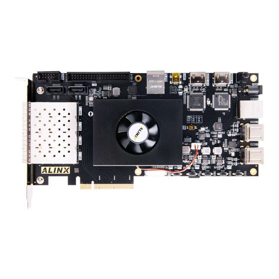
AX7Z035B User Manual 1. Development Board Introduction The entire structure of AX7Z035B FPGA development board is inherited from our consistent core board+carrier board model. A high-speed inter-board connector is used between the core board and the carrier board. The core board is mainly composed of ZYNQ7035 + 4x DDR3 + eMMC + QSPI FLASH. - Page 5 AX7Z035B User Manual Through this diagram, you can see the interfaces and functions that the AX7Z035B FPGA Development Board contains: ZYNQ7035 core board The core board consists of XC7Z035+2GB DDR3+8GB eMMC FLASH + 512Mb QSPI FLASH. In addition, three crystal oscillators provide clocks: one single-ended 33.3333MHz crystal oscillator to the PS system, one differential 200MHz crystal...
- Page 6 1x Micro SD card holder, used to store operating system images and file systems. 40-pin Expansion Port A 40-pin 2.54mm pitch expansion port can be connected to various ALINX modules (binocular camera, TFT LCD screen, high-speed AD module, etc.). The expansion port contains 1x 5V power supply, 2x 3.3V power supply, 3x ground, 34x...
-
Page 7: Ac7Z035B Core Board
AX7Z035B User Manual 2. AC7Z035B Core Board 2.1 Introduction AC7Z035B (core board model, the same below) FPGA core board, ZYNQ chip is based on XC7Z035-2FFG676 of XILINX company ZYNQ7000 series. The ZYNQ chip's PS system integrates two ARM Cortex -A9 processors, AMBA® interconnects, internal memory, external memory interfaces and peripherals. - Page 8 AX7Z035B User Manual AC7Z035B Front View AC7Z035B Back View www.alinx.com 8 / 58...
-
Page 9: Zynq Chip
AX7Z035B User Manual 2.2 ZYNQ Chip The FPGA core board AC7Z035B uses Xilinx's Zynq7000 series chip, model XC7Z035-2FFG676. The chip's PS system integrates two ARM CortexTM-A9 processors, AMBA® interconnects, internal memory, external memory interfaces and peripherals. These peripherals mainly include USB bus interface, Ethernet interface, SD/SDIO interface, I2C bus interface, CAN bus interface, UART interface, GPIO etc. - Page 10 AX7Z035B User Manual 2x SD card, SDIO, MMC compatible controllers. 2x SPIs, 2x UARTs, 2x I2C interfaces. 54x multi-function Ios, which can be configured as normal IO or peripheral control interfaces. High bandwidth connection within PS and PS to PL.
-
Page 11: Ddr3 Dram
Figure 2-2-3: The XC7Z035 chip used on the Core Board 2.3 DDR3 DRAM The FPGA board AX7Z035B is equipped with four Micron 512MB DDR3 chips, model MT41J256M16HA-125 (compatible with MT41K256M16HA-125), each side has 2 DDR3s mounted. Two DDR3 SDRAMs form a 32-bit bus width. The PS-side... - Page 12 AX7Z035B User Manual control, and line length control in circuit design and PCB design to ensure high- speed and stable operation of DDR3. The hardware connection of DDR3 DRAM on the PS side is shown in Figure 2-3- Upper 16bits data 数据高16位...
- Page 13 AX7Z035B User Manual PS DDR3 DRAM 拼 assignment: Signal Name ZYNQ Pin Name ZYNQ Pin Number PS_DDR3_DQS0_P PS_DDR_DQS_P0_502 PS_DDR3_DQS0_N PS_DDR_DQS_N0_502 PS_DDR3_DQS1_P PS_DDR_DQS_P1_502 PS_DDR3_DQS1_N PS_DDR_DQS_N1_502 PS_DDR3_DQS2_P PS_DDR_DQS_P2_502 PS_DDR3_DQS2_N PS_DDR_DQS_N2_502 PS_DDR3_DQS3_P PS_DDR_DQS_P3_502 PS_DDR3_DQS4_N PS_DDR_DQS_N3_502 PS_DDR3_D0 PS_DDR_DQ0_502 PS_DDR3_D1 PS_DDR_DQ1_502 PS_DDR3_D2 PS_DDR_DQ2_502 PS_DDR3_D3 PS_DDR_DQ3_502...
- Page 14 AX7Z035B User Manual PS_DDR3_D22 PS_DDR_DQ22_502 PS_DDR3_D23 PS_DDR_DQ23_502 PS_DDR3_D24 PS_DDR_DQ24_502 PS_DDR3_D25 PS_DDR_DQ25_502 PS_DDR3_D26 PS_DDR_DQ26_502 PS_DDR3_D27 PS_DDR_DQ27_502 PS_DDR3_D28 PS_DDR_DQ28_502 PS_DDR3_D29 PS_DDR_DQ29_502 PS_DDR3_D30 PS_DDR_DQ30_502 PS_DDR3_D31 PS_DDR_DQ31_502 PS_DDR3_DM0 PS_DDR_DM0_502 PS_DDR3_DM1 PS_DDR_DM1_502 PS_DDR3_DM2 PS_DDR_DM2_502 PS_DDR3_DM3 PS_DDR_DM3_502 PS_DDR3_A0 PS_DDR_A0_502 PS_DDR3_A1 PS_DDR_A1_502 PS_DDR3_A2 PS_DDR_A2_502 PS_DDR3_A3 PS_DDR_A3_502 PS_DDR3_A4...
- Page 15 AX7Z035B User Manual PS_DDR3_S0 PS_DDR_CS_B_502 PS_DDR3_RAS PS_DDR_RAS_B_502 PS_DDR3_CAS PS_DDR_CAS_B_502 PS_DDR3_WE PS_DDR_WE_B_502 PS_DDR3_ODT PS_DDR_ODT_502 PS_DDR3_RESET PS_DDR_DRST_B_502 PS_DDR3_CLK0_P PS_DDR_CKP_502 PS_DDR3_CLK0_N PS_DDR_CKN_502 PS_DDR3_CKE PS_DDR_CKE_502 PL DDR3 DRAM pin assignment: Signal Name ZYNQ Pin Name ZYNQ Pin Number PL_DDR3_DQS0_P IO_L3P_T0_DQS_33 PL_DDR3_DQS0_N IO_L3N_T0_DQS_33 PL_DDR3_DQS1_P IO_L9P_T1_DQS_33...
- Page 16 AX7Z035B User Manual PL_DDR3_D12 IO_L11N_T1_SRCC_33 PL_DDR3_D13 IO_L8P_T1_33 PL_DDR3_D14 IO_L11P_T1_SRCC_33 PL_DDR3_D15 IO_L10P_T1_33 PL_DDR3_D16 IO_L18P_T2_33 PL_DDR3_D17 IO_L14P_T2_SRCC_33 PL_DDR3_D18 IO_L14N_T2_SRCC_33 PL_DDR3_D19 IO_L13P_T2_MRCC_33 PL_DDR3_D20 IO_L16P_T2_33 PL_DDR3_D21 IO_L17P_T2_33 PL_DDR3_D22 IO_L16N_T2_33 PL_DDR3_D23 IO_L17N_T2_33 PL_DDR3_D24 IO_L23P_T3_33 PL_DDR3_D25 IO_L22N_T3_33 PL_DDR3_D26 IO_L19P_T3_33 PL_DDR3_D27 IO_L20N_T3_33 PL_DDR3_D28 IO_L24P_T3_33 PL_DDR3_D29 IO_L20P_T3_33 PL_DDR3_D30...
-
Page 17: Qspi Flash
AX7Z035B User Manual PL_DDR3_A8 IO_L12N_T1_MRCC_34 PL_DDR3_A9 IO_L18N_T2_34 PL_DDR3_A10 IO_L24N_T3_34 PL_DDR3_A11 IO_L11P_T1_SRCC_34 PL_DDR3_A12 IO_L23N_T3_34 PL_DDR3_A13 IO_L16P_T2_34 PL_DDR3_A14 IO_L12P_T1_MRCC_34 PL_DDR3_BA0 IO_L18P_T2_34 PL_DDR3_BA1 IO_L19N_T3_VREF_34 PL_DDR3_BA2 IO_L22N_T3_34 PL_DDR3_S0 IO_L14N_T2_SRCC_34 PL_DDR3_RAS IO_L19P_T3_34 PL_DDR3_CAS IO_L20N_T3_34 PL_DDR3_WE IO_L20P_T3_34 PL_DDR3_ODT IO_L22P_T3_34 PL_DDR3_RESET IO_L16N_T2_34 PL_DDR3_CLK0_P IO_L21P_T3_DQS_34 PL_DDR3_CLK0_N IO_L21N_T3_DQS_34 PL_DDR3_CKE IO_L24P_T3_34 2.4 QSPI Flash... - Page 18 AX7Z035B User Manual QSPI FLASH is connected to the GPIO port of the PS BANK500 of the ZYNQ chip. In the system design, the functions of these PS GPIO ports need to be configured as the QSPI FLASH interfaces. Figure 2-4-1 shows the QSPI Flash in the schematic.
-
Page 19: Emmc Flash
AX7Z035B User Manual QSPI1_D3 PS_MIO13_500 2.5 eMMC Flash The FPGA core board AC7Z035B is equipped with a large-capacity 8GB eMMC FLASH chip, model THGBMFG6C1LBAIL, which supports the JEDEC e-MMC V5.0 standard HS-MMC interface with level of 1.8V or 3.3V. The data width of the connection between eMMC FLASH and ZYNQ is 4 bits. -
Page 20: Clock Configuration
AX7Z035B User Manual Signal Name ZYNQ Pin Name ZYNQ Pin Number MMC_CCLK PS_MIO48_501 MMC_CMD PS_MIO47_501 MMC_D0 PS_MIO46_501 MMC_D1 PS_MIO49_501 MMC_D2 PS_MIO50_501 MMC_D3 PS_MIO51_501 2.6 Clock Configuration The core system respectively provides reference clocks for the PS system, the PL logic, and the GTX transceiver, allowing the PS system and PL logic to work independently. - Page 21 AX7Z035B User Manual Figure 2-6-2: PS active crystal oscillator Clock pin assignment: Signal Name ZYNQ Pin PS_CLK PL system clock source The board has a differential 200MHz PL system clock source for the reference clock of the DDR3 controller. The crystal output is connected to the MRCC of the FPGA BANK34, which can be used to drive the DDR3 controller and user logic in the FPGA.
- Page 22 AX7Z035B User Manual PL clock pin assignment: Signal Name ZYNQ Pin SYS_CLK_P SYS_CLK_N GTX reference clock The FPGA core board provides a 125Mhz reference clock for the GTX transceiver. The reference clock is connected to the reference clock input REFCLK1P/REFCLK1N of the BANK111. The schematic diagram of the clock source is...
-
Page 23: Led Light
AX7Z035B User Manual 2.7 LED Light There are 3 red LED lights on the AC7Z035B FPGA core board, one of which is the power indicator light (PWR), one is the configuration LED light (DONE), and one is the user LED light. When the core board is powered, the power indicator will light up;... - Page 24 AX7Z035B User Manual Figure 2-8-1: Reset connection diagram Reset key ZYNQ pin assignment: Signal Name ZYNQ Pin Name ZYNQ Pin No. Description PS_POR_B PS_POR_B_500 ZYNQ System Reset Signal www.alinx.com 24 / 58...
-
Page 25: Power Supply
AX7Z035B User Manual 2.9 Power Supply The power supply voltage of the AC7Z035B core board is DC5V, which is supplied by connecting the carrier board. The schematic diagram of the power supply design on the board is shown in Figure 2-9-1: +1.0V/20A... - Page 26 AX7Z035B User Manual BANK12 and BANK13 is generated through two SPX3819M5-3-3 channels. Users can replace the LDO chip to make the IO input and output of these two BANKs meet other voltage standards. The functions of each power distribution are shown in the following table:...
-
Page 27: Size Dimension
AX7Z035B User Manual 2.10 Size Dimension Top View 2.11 Connectors Pin Assignment The core board has a total of 4 high-speed expansion ports, which are connected to the carrier board using four 120Pin board-to-board connectors (J29~J32). The connectors use Panasonic's AXK5A2137YG, and the corresponding connectors' model on the carrier board is AXK6A2337YG. - Page 28 AX7Z035B User Manual B13_L10_N AA23 B13_L13_N AD21 B13_L10_P AA22 B13_L13_P AD20 B13_L15_N AF20 B13_L14_N AC22 B13_L15_P AF19 B13_L14_P AC21 B13_L23_N B13_L7_P AE22 B13_L23_P B13_L7_N AF22 B13_L22_P AA19 B13_L20_P AA20 B13_L22_N AB19 B13_L20_N AB20 B13_L17_N AD19 B13_L18_N AF18 B13_L17_P AD18 B13_L18_P...
- Page 29 AX7Z035B User Manual B12_L4_P AB11 B12_L20_P AB17 B12_L4_N AB10 B12_L20_N AB16 B12_L7_P AE10 B12_L8_N AF12 B12_L7_N AD10 B12_L8_P AE12 B12_L24_P B12_L21_P AC17 B12_L24_N B12_L21_N AC16 B12_L3_N AA10 B12_L17_P AE16 B12_L3_P B12_L17_N AE15 B12_L11_P AC12 B12_L22_P AA15 B12_L11_N AD11 B12_L22_N AA14...
- Page 30 AX7Z035B User Manual BANK112_TX0_N BANK112_RX0_N BANK112_TX0_P BANK112_RX0_P BANK112_TX1_N BANK112_RX1_N BANK112_TX1_P BANK112_RX1_P BANK112_TX2_N BANK112_RX2_N BANK112_TX2_P BANK112_RX2_P BANK112_TX3_N BANK112_RX3_N BANK112_TX3_P BANK112_RX3_P BANK112_CLK0_N BANK112_CLK1_N BANK112_CLK0_P BANK112_CLK1_P BANK111_RX3_N BANK111_RX3_P BANK111_TX3_N BANK111_TX3_P www.alinx.com 30 / 58...
- Page 31 AX7Z035B User Manual BANK111_RX2_N BANK111_RX2_P BANK111_TX2_N BANK111_TX2_P BANK111_RX1_N BANK111_RX1_P BANK111_TX1_N BANK111_TX1_P BANK111_RX0_N BANK111_RX0_P BANK111_TX0_N BANK111_TX0_P BANK111_CLK0_N BANK111_CLK0_P J31 connector pin assignment: J31 Pin Signal ZYNQ J31 Pin Signal Name ZYNQ Pin Name Pin No. FPGA_TCK FPGA_TDI FPGA_TMS FPGA_TDO www.alinx.com 31 / 58...
- Page 32 AX7Z035B User Manual B35_L3_P B35_L2_P B35_L3_N B35_L2_N B35_L7_N B35_L6_P B35_L7_P B35_L6_N B35_L4_P B35_L23_P B35_L4_N B35_L23_N B35_L5_N B35_L22_P B35_L5_P B35_L22_N B35_L8_P B35_L24_N B35_L8_N B35_L24_P B35_L12_P B35_L11_N B35_L12_N B35_L11_P B35_L9_P B35_L19_N B35_L9_N B35_L19_P B35_L1_N B35_L21_N B35_L1_P B35_L21_P B35_L17_N B35_L14_P B35_L17_P B35_L14_N B35_L20_N...
- Page 33 AX7Z035B User Manual B35_L13_N B35_L13_P B35_L16_N B35_L16_P PS_POR_B SYS_RESET J32 connector pin assignment: J32 Pin Signal ZYNQ J32 Pin Signal Name ZYNQ Pin Name Pin No. PS_MIO5 PS_MIO17 PS_MIO4 PS_MIO18 www.alinx.com 33 / 58...
- Page 34 AX7Z035B User Manual PS_MIO14 PS_MIO19 PS_MIO15 PS_MIO20 PS_MIO52 PS_MIO16 PS_MIO53 PS_MIO21 PS_MIO7 PS_MIO26 PS_MIO25 PS_MIO40 PS_MIO24 PS_MIO41 PS_MIO23 PS_MIO42 PS_MIO27 PS_MIO43 PS_MIO22 PS_MIO44 PS_MIO30 PS_MIO45 PS_MIO29 PS_MIO36 PS_MIO31 PS_MIO32 PS_MIO33 PS_MIO34 PS_MIO35 PS_MIO28 PS_MIO37 PS_MIO38 PS_MIO39 www.alinx.com 34 / 58...
- Page 35 AX7Z035B User Manual B13_L1_P AA25 B13_L11_P AD23 B13_L1_N AB25 B13_L11_N AD24 B13_L6_P AA24 B13_L4_P AD25 B13_L6_N AB24 B13_L4_N AD26 B13_L2_N AC26 B13_L5_P AF24 B13_L2_P AB26 B13_L5_N AF25 B13_L12_P AC23 B13_L3_P AE25 B13_L12_N AC24 B13_L3_N AE26 www.alinx.com 35 / 58...
-
Page 36: Carrier Board
4x LED Lights 3.2 Uart to USB Interface The AX7Z035B carrier board is equipped with a Uart to USB interface for system debugging. The conversion chip uses the USB-UAR chip of Silicon Labs CP2102GM. The USB interface uses the MINI USB interface. It can be connected to the USB port of the upper PC with a USB cable for separate power supply and serial data communication of the core board. -
Page 37: Gigabit Ethernet Interface
Uart data output 3.3 Gigabit Ethernet Interface The AX7Z035B development board has two Gigabit Ethernet interfaces, one of which is connected to the PS system, and the other one is connected to the logical IO ports of the PL. The Gigabit Ethernet interface connected to the PL side needs to be mounted to ZYNQ's AXI bus system via program calling IP. - Page 38 AX7Z035B User Manual BANK501. The Ethernet PHY chip on the PL end is connected to the IO of BANK35. The JL2121 chip supports a 10/100/1000 Mbps network transmission rate and communicates data with the MAC layer of the Zynq7000 system through the RGMII interface.
- Page 39 AX7Z035B User Manual PHY1_TXCK PHY1_TXCTL PHY1_TXD0~PHY1_TXD3 PHY1_RXCK ZYNQ GPHY PHY1_RXCTL (JL2121) PHY1_TXD0~PHY1_RXD3 PHY1_MDC PHY1_MDIO PHY1_RESET Figure 3-3-1: Connection between ZYNQ PS system and GPHY Figure 3-3-2 shows the connection diagram of the ZYNQ PL Ethernet PHY chip: Figure 3-3-2: Connection between ZYNQ PL and GPHY www.alinx.com...
- Page 40 AX7Z035B User Manual PS side Gigabit Ethernet pin assignment: Signal Name ZYNQ Pin Name ZYNQ Pin Number Description PHY1_TXCK PS_MIO16_501 RGMII Transmit Clock PHY1_TXD0 PS_MIO17_501 Transmit data bit0 PHY1_TXD1 PS_MIO18_501 Transmit data bit1 PHY1_TXD2 PS_MIO19_501 Transmit data bit2 PHY1_TXD3 PS_MIO20_501...
-
Page 41: Usb2.0 Host Interface
Reset signal 3.4 USB2.0 Host Interface There are 4 USB2.0 HOST interfaces on the AX7Z035B FPGA development board. The USB2.0 transceiver uses a 1.8V, high-speed USB3320C-EZK chip that supports the ULPI standard interface, and then expands the 4-way USB HOST interfaces through a USB HUB chip USB2514. -
Page 42: Hdmi Output Interface
AX7Z035B User Manual Figure 3-4-1: The connection between Zynq7000 and USB chips USB2.0 pin assignment: Signal Name ZYNQ Pin Name ZYNQ Pin Description Number OTG_DATA4 PS_MIO28_501 USB Data Bit4 OTG_DIR PS_MIO29_501 USB Data Direction Signal OTG_STP PS_MIO30_501 USB Stop Signal... - Page 43 AX7Z035B User Manual I2C configuration interface are connected to the PL BANK35 IO of the ZYNQ7000. The ZYNQ7000 system initializes and controls the ADV7511 through the I2C pin. The hardware connection diagram of ADV7511 chip and ZYNQ7000 is shown in Figure 3- 5-1.
-
Page 44: Hdmi Input Interface
AX7Z035B User Manual HDMI_D6 B35_L8_N HDMI video signal data 6 HDMI_D7 B35_L12_P HDMI video signal data 7 HDMI_D8 B35_L12_N HDMI video signal data 8 HDMI_D9 B35_L9_N HDMI video signal data 9 HDMI_D10 B35_L1_N HDMI video signal data 10 HDMI_D11 B35_L1_P... - Page 45 AX7Z035B User Manual 9013_CLK QDCK 9013_DE 9013_HS HSYNC 9013_VS VSYNC 9013_D[23:16] ZYNQ QE[23:16] TDMS 9013_D[15:8] QE[15:8] 9013_D[7:0] QE[7:0] 9013_SCL CSCL 9013_SDA CSDA 9013_nRESET RESET# Figure 3-6-1: HDMI input schematic diagram ZYNQ pin assignment: Signal Name ZYNQ Pin Name ZYNQ Pin...
-
Page 46: Sfp Interface
3.7 SFP Interface The AX7Z035B carrier board has four SFP interfaces. Users can purchase SFP optical modules (1.25G, 2.5G, 10G optical modules on the market) and insert them into these four interfaces for optical data communication. The four SFP interfaces are connected to the two RX/TX of the GNK transceiver of ZYNQ BANK111. - Page 47 AX7Z035B User Manual Figure 3-7-1: Schematic diagram of fiber optic design Pin assignment of 4 SFP interfaces: Signal Name ZYNQ Pin Name ZYNQ Pin Description Number SFP1_TX_P Optical module 1 transmit data BANK111_TX0_P positive SFP1_TX_N Optical module 1 transmit data...
-
Page 48: Pcie Slot
3.8 PCIe Slot The AX7Z035B carrier board has a PCIe x4 interface. In order to be compatible with the AC7Z100 core board, the PCB is physically made into a PCIE x8 interface. In the electrical connection, we only have 4 pairs of transceivers connected to the PCIEx8 slot, so only PCIEex4, PCIex2, PCIex1 data communication can be realized. - Page 49 AX7Z035B User Manual ZYNQ Figure 3-8-1: PCIe slot design schematic PCIe x4 interface ZYNQ pin assignment: Signal Name ZYNQ Pin Name ZYNQ Pin Description Number PCIE_RX0_P PCIE Channel 0 Data Receive BANK112_RX3_P Positive PCIE_RX0_N PCIE Channel 0 Data Receive BANK112_RX3_N...
-
Page 50: Sd Card Slot
PCIE board reset signal 3.9 SD Card Slot The AX7Z035B FPGA board contains a Micro SD card interface to provide user access to the SD card memory, the BOOT program for storing the ZYNQ chip, the Linux operating system kernel, the file system and other user data files. -
Page 51: 40Pin Expansion Port
The carrier board is reserved with one 2.54-mm standard 40-pin expansion ports J33, which are used to connect the ALINX modules or the external circuit designed by the user himself. The expansion port has 40 signals with 1x 5V power supply, 2x 3.3 V power supply, 3x ground and 34x IO. - Page 52 AX7Z035B User Manual Figure 3-10-1: J33 schematic diagram J33 ZYNQ pin assignment: J33 Pin Signal Name ZYNQ J33 Pin Signal Name ZYNQ Pin No. Pin No. IO1_1N IO1_1P IO1_2N AC11 IO1_2P AB12 IO1_3N AA12 IO1_3P AA13 IO1_4N AF10 IO1_4P AE11...
-
Page 53: Led Light
AX7Z035B User Manual IO1_14N AE12 IO1_14P AF12 IO1_15N AB10 IO1_15P AB11 IO1_16N AB16 IO1_16P AB17 IO1_17N AA17 IO1_17P +3.3V +3.3V 3.11 LED Light There are 7 LEDs on the carrier board, including 1x power indicator, 2x serial communication indicators and 4x PL control indicators. When the board is powered on, the power indicator will light up;... -
Page 54: Reset Key And User Key
User PL LED4 3.12 Reset Key and User Key The AX7Z035B has a reset key “RESET” and 4 user keys on the carrier board. The reset signal is connected to the reset chip input of the core board. Users can use this reset key to reset the ZYNQ system. -
Page 55: Jtag Debugging Port
AX7Z035B User Manual 3.13 JTAG Debugging Port A JTAG interface is reserved on the carrier board for downloading ZYNQ programs or solidifying programs to FLASH. To prevent damage to the ZYNQ chip caused by hot-plugging or unplugging, we have added protective diodes to the JTAG signal to ensure that the signal voltage is within the range accepted by the FPGA and avoid damage to the ZYNQ chip. -
Page 56: Power Supply
AX7Z035B User Manual Dip Position(1, 2) MIO5, MIO4 Level Boot Mode ON、ON 0、0 JTAG OFF、OFF 1、1 SD Card OFF、ON 1、0 QSPI FLASH Figure 3-14-1: SW1 boot mode configuration 3.15 Power Supply The power input voltage of the development board is DC12V. You can supply power to the development board through the PCIE slot or external +12V power supply. -
Page 57: Fan
AX7Z035B User Manual +1.8V Ethernet,HDMI,USB +3.3V Ethernet,HDMI,USB,SD,SFP,PCIE 3.16 Fan Because ZYNQ7035 generates a lot of heat when it is working properly, we added a heat sink and fan to the board to prevent the chip from overheating. Fan control is controlled by ZYNQ chip, the control pin is connected to the IO of BANK12. -
Page 58: Size Dimension
AX7Z035B User Manual 3.17 Size Dimension Figure 3-17-1: Top View www.alinx.com 58 / 58...
Need help?
Do you have a question about the AX7Z035B and is the answer not in the manual?
Questions and answers