Table of Contents
Advertisement
Quick Links
Advertisement
Table of Contents

Related Manuals for Alinx AX7102


Summary of Contents for Alinx AX7102
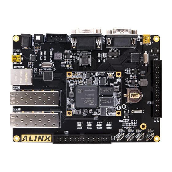
- Page 1 ALINX FPGA BOARD AX7102 User Manual...
- Page 2 AX7102 User Manual Copyright Notice: Copyright ©2018 by ALINX Technologies inc. All rights are reserved. Development Environment: Vivado 2015.4 is from Xilinx website https://www.xilinx.com Official website: Http://www.alinx.com.cn E-mail: avic@alinx.com.cn Tel: +86-021-67676997 WeChat public number: ALINX-HEIJIN Http://www.alinx.com.cn 2 / 59...
-
Page 3: Table Of Contents
AX7102 User Manual Contents 一、 Overview ......................... 6 二、 FPGA Core Board ....................8 (一) Overview ......................8 (二) FPGA ........................9 (三) CLOCK ......................11 (四) DDR3 ....................... 14 (五) QSPI Flash ...................... 17 (六) LEDs ......................... 19 (七) RESET Button .................... - Page 4 AX7102 User Manual (十四) LED ........................56 (十五) POWER......................57 Http://www.alinx.com.cn 4 / 59...
- Page 5 AX7102 User Manual The AX7102 development Kit presents a robust hardware design platform built around the XILINX Artix-7 FPGA, which optimized for lowest cost and power with small form-factor packaging for the highest volume applications. The AX7102 development board is equipped with high-speed DDR3 memory, SFP networking, and USB2.0 capabilities, Ethernet networking, and much more...
-
Page 6: 一、 Overview
DDR3 and QSPI FLASH. The expansion board extends the many peripheral interface for core board, which contains SFP fiber interface, gigabit Ethernet network port, USB2.0 port, VGA port and etc. Figure 1-2 provides a quick overview of the block diagram of AX7102 board. USB2.0 RS232... - Page 7 AX7102 User Manual The following hardware resources are provided on the AX7102 board: Features of FPGA Core Board: FPGA Device XILINX ARTIX-7 FPGA XC7A100T ; 101,440 Logic Cells; 240 DSP48 Slices include 18 x 18 multiplier, an adder, and accumulator;...
-
Page 8: 二、 Fpga Core Board
AX7102 User Manual 24-bit DAC of VGA output ; Buttons and Indicators 5 User LEDs and (one is on core board); 5 user Buttons (one button acts as reset button on core board); 二、 FPGA Core Board (一) Overview... -
Page 9: (二) Fpga
AX7102 User Manual Figure2-1-1 AC7100 TOP View Figure 2-1-2 AC7100 Bottom View (二) FPGA AC7100 Core board uses Xilinx Artix-7 FPGA device, the detail part number is Http://www.alinx.com.cn 9 / 59... - Page 10 AX7102 User Manual XC7A100T-2FGG484I. The Xilinx Artix-7 FPGA ordering information is shown in Figure 2-2-1. Figure 2-2-1 Artix-7 Ordering Information Figure 2-2-2 shows the FPGA chipset on AC7100 core board. Figure 2-2-2 FPGA Chipset The feature summary of XC7A100T is listed as following:...
-
Page 11: Clock
AX7102 User Manual CMTs PCIe Gen2 XADC 1 个 12bit, 1Mbps AD GTP Transceiver 4 个,6.6Gb/s max Speed Operation Temperate -40 ~ 85degree FPGA Power Supply Artix-7 FPGA has six power supplies including V CCINT CCBRAM CCAUX and V is the core power supply of FPGA and should be... - Page 12 AX7102 User Manual This 200Mhz system clock can produce different frequency clock to drive the user logic thought PLLs and DCMs inside FPGA. Figure 2-3-1 200Mhz System Clock Figure 2-3-2 shows the onboard 200Mhz differential crystal oscillator Figure 2-3-2 Onboard 200Mhz Crystal Oscillator Clock Pin Assignment.
- Page 13 AX7102 User Manual 2). 148.5Mhz Differential Crystal Oscillator The Figure 2-3-3 is the circuit of 148.5Mhz clock for GPT transceiver. The output of differential crystal oscillator is connected to MGTREFCLK0P pin(F6) and MGTREFCLK0N pin(E6) of FPGA bank216. Figure 2-3-3 148.5Mhz Differential Crystal Oscillators Figure 2-3-4 shows the onboard 148.5Mhz differential crystal oscillator.
-
Page 14: (四) Ddr3
AX7102 User Manual (四) DDR3 The core board features 1GB of DDR3 memory, implemented using two 512MB DDR3 devices. The data bandwidth is in 32-bit, comprised of two x16 devices with a single address/command bus. the target clock speed for FPGA and DDR3 is 800 MHz(Data rate is 1600M). - Page 15 AX7102 User Manual Figure 2-4-2 DDR3 SDRAM Onboard DDR3 SDRAM PIN Assignment: Net Name FPGA PIN Name FPGA P/N DDR3_DQS0_P IO_L3P_T0_DQS_AD5P_35 DDR3_DQS0_N IO_L3N_T0_DQS_AD5N_35 DDR3_DQS1_P IO_L9P_T1_DQS_AD7P_35 DDR3_DQS1_N IO_L9N_T1_DQS_AD7N_35 DDR3_DQS2_P IO_L15P_T2_DQS_35 DDR3_DQS2_N IO_L15N_T2_DQS_35 DDR3_DQS3_P IO_L21P_T3_DQS_35 DDR3_DQS3_N IO_L21N_T3_DQS_35 DDR3_DQ[0] IO_L2P_T0_AD12P_35 DDR3_DQ [1] IO_L5P_T0_AD13P_35...
- Page 16 AX7102 User Manual DDR3_DQ [4] IO_L2N_T0_AD12N_35 DDR3_DQ [5] IO_L5N_T0_AD13N_35 DDR3_DQ [6] IO_L1P_T0_AD4P_35 DDR3_DQ [7] IO_L4P_T0_35 DDR3_DQ [8] IO_L11P_T1_SRCC_35 DDR3_DQ [9] IO_L11N_T1_SRCC_35 DDR3_DQ [10] IO_L8P_T1_AD14P_35 DDR3_DQ [11] IO_L10N_T1_AD15N_35 DDR3_DQ [12] IO_L7N_T1_AD6N_35 DDR3_DQ [13] IO_L10P_T1_AD15P_35 DDR3_DQ [14] IO_L7P_T1_AD6P_35 DDR3_DQ [15] IO_L12P_T1_MRCC_35 DDR3_DQ [16]...
-
Page 17: Qspi Flash
AX7102 User Manual DDR3_DM3 IO_L23N_T3_35 DDR3_A[0] IO_L11N_T1_SRCC_34 DDR3_A[1] IO_L8N_T1_34 DDR3_A[2] IO_L10P_T1_34 DDR3_A[3] IO_L10N_T1_34 DDR3_A[4] IO_L7N_T1_34 DDR3_A[5] IO_L6P_T0_34 DDR3_A[6] IO_L5P_T0_34 DDR3_A[7] IO_L1P_T0_34 DDR3_A[8] IO_L2N_T0_34 DDR3_A[9] IO_L2P_T0_34 DDR3_A[10] IO_L5N_T0_34 DDR3_A[11] IO_L4P_T0_34 DDR3_A[12] IO_L4N_T0_34 DDR3_A[13] IO_L1N_T0_34 DDR3_A[14] IO_L6N_T0_VREF_34 DDR3_BA[0] IO_L9N_T1_DQS_34 DDR3_BA[1] IO_L9P_T1_DQS_34 DDR3_BA[2]... - Page 18 AX7102 User Manual bus. The flash device is N25Q128 which uses 3.3V CMOS signaling standard. Because of its non-volatile property, it is usually used for storing software binaries, images, sounds or other media. Detail information of QSPI FLASH is shown in table 2-5-1 below.
-
Page 19: (六) Leds
AX7102 User Manual Figure 2-5-2 shows onboard QSPI FLASH. Figure 2-5-2 QSPI FLASH Onboard (六) LEDs There are three RED LEDs on the FPGA, it includes power indicator LED, done indicator LED and user LED. When the core board is power on, the power indicator LED turns on. -
Page 20: Reset Button
AX7102 User Manual Figure 2-6-2 LEDs on AC7100 board Pin Assignment of User LED Net Name FPGAPIN Name FPGA P/N Comment LED1 IO_L15N_T2_DQS_34 User LED (七) RESET Button AC7100 core board has a reset button, it is connected to the bank34 IO of FPGA. -
Page 21: Jtag Interface
AX7102 User Manual Figure 2-7-2 Reset Button on AC7100 Board Pin Assignment of Reset Button Net Name FPGAPIN Name FPGA P/N Comment RESET_N IO_L17N_T2_34 复位按键Reset (八) JTAG Interface In the AC7100 core board, it reserves a JTAG interface (J1), it is used to download or debug FPGA program without expansion board. -
Page 22: Power Input
AX7102 User Manual Figure 2-8-2 JTAG Interface On Board (九) Power Input In AC7100 core board, we reserved a mini USB port(J2) which can power on core board and work separately without expansion board. Using a USB cable connect to computer, the +5.0V power supply is coming from USB port to power on AC7100 board. -
Page 23: (十) Board-To-Board Connector
AX7102 User Manual Figure 2-9-2 MINI USB port on AC7100 board (十) Board-to-Board Connector The core board has four high-speed board-to-board connectors on PCB bottom side. Each connector is 80-pins of 0.5mm pin pitch, which is suitable for high-speed signal transmission. 180 FPGA IOs (include 86 pairs LVDS signals) and all differential signals of GTP transceivers are connected to expansion board through these four connectors. - Page 24 AX7102 User Manual B13_L4_P AA15 3.3V B13_L4_N AB15 3.3V Ground Ground B13_L5_P 3.3V B13_L1_P 3.3V B13_L5_N AA14 3.3V B13_L1_N AA16 3.3V B13_L7_P AB11 3.3V B13_L2_P AB16 3.3V B13_L7_P AB12 3.3V B13_L2_N AB17 3.3V Ground Ground B13_L3_P AA13 3.3V B13_L6_P 3.3V...
- Page 25 AX7102 User Manual B16_L6_P 3.3V B16_L8_P 3.3V B16_L8_N 3.3V Figure 2-10-1 is the CON1 connector on core board, and the pin1 of connector is marked on the board. Figure 2-10-1 CON1 Connector Onboard CON2 Connector The 80-Pin connector CON2 is used to extend the IOs of FPGA bank13 and bank14, the voltage level of these IOs are +3.3V standard.
- Page 26 AX7102 User Manual Ground Ground B13_L11_P 3.3V B14_L15_N AB20 3.3V B13_L11_N 3.3V B14_L15_P AA19 3.3V B13_L10_P 3.3V B14_L17_P AA18 3.3V B13_L10_N 3.3V B14_L17_N AB18 3.3V Ground Ground B13_L9_N AA11 3.3V B14_L6_N 3.3V B13_L9_P AA10 3.3V B13_IO0 3.3V B13_L8_N AB10 3.3V B14_L7_N 3.3V...
- Page 27 AX7102 User Manual Figure 2-10-2 is the CON2 connector on core board, and the pin1 of connector is marked on the board. Figure 2-10-2 CON2 Connector Onboard CON3 Connector The 80-Pin connector CON3 is used to extend the IOs of FPGA bank15 and bank16, the voltage level of these IOs are +3.3V standard by default, but it can...
- Page 28 AX7102 User Manual B15_L12_N 3.3V B16_L22_N 3.3V Ground Ground B15_L11_P 3.3V B16_L24_P 3.3V B15_L11_N 3.3V B16_L24_N 3.3V B15_L1_N 3.3V B15_L8_N 3.3V B15_L1_P 3.3V B15_L8_P 3.3V Ground Ground B15_L5_P 3.3V B15_L7_N 3.3V B15_L5_N 3.3V B15_L7_P 3.3V B15_L3_N 3.3V B15_L9_P 3.3V B15_L3_P 3.3V...
- Page 29 AX7102 User Manual FPGA_TDO 3.3V FPGA_TMS 3.3V Figure 2-10-3 is the CON3 connector on core board, and the pin1 of connector is marked on the board. Figure 2-10-3 CON3 Connector Onboard CON4 Connector The 80-Pin connector CON4 is used to extend the IOs of FPGA bank16 and signals of GTP transceivers.
- Page 30 AX7102 User Manual MGT_RX3_P Diff MGT_TX0_P Diff MGT_RX3_N Diff MGT_TX0_N Diff Ground Ground MGT_TX1_P Diff MGT_RX0_P Diff MGT_TX1_N Diff MGT_RX0_N Diff Ground Ground MGT_RX1_P Diff MGT_CLK1_P Diff MGT_RX1_N Diff MGT_CLK1_N Diff Ground Ground B16_L5_P 3.3V B16_L2_P 3.3V B16_L5_N 3.3V B16_L2_N 3.3V...
-
Page 31: (十一) Power
AX7102 User Manual Figure 2-10-4 CON4 Connector Onboard (十一) POWER The power supply voltage of the AC7100 core board is DC5V and can supply from mini USB port or board-to-board connector from expansion board. Please note that the mini USB and expansion board cannot supply power to core board at the same time, it maybe damage the USB port of computer. - Page 32 AX7102 User Manual Figure 2-11-1Power Design AC7100 core board uses the +5V power to generate +3.3V, +1.5V, +1.8V and +1.0V power output through the DC/DC power convertor. The output current of each power can be as high as 3A. AC7100 core board uses a LDO chipset of SPX3819M5-3-3 to generate +3.3V power supply for VCCIO power of FPGA...
- Page 33 AX7102 User Manual Power circuit on AC7100 core board is showed in Figure 2-11-2 below. Figure 2-11-2 Power of AC7100 Http://www.alinx.com.cn 33 / 59...
-
Page 34: (十二) Mechanical
AX7102 User Manual (十二) Mechanical Top View Bottom View Http://www.alinx.com.cn 34 / 59... -
Page 35: 三、 Expansion Board
AX7102 User Manual 三、 Expansion Board (一) Overview The following features are provided on the AX7102 expansion board: One 10/100M/1000M Ethernet with RJ45 port; Two Port of SFP port;; One USB2.0 Port; One USB-to-serial port; One RS232 Serial Port;... -
Page 36: Gigabit Ethernet
Gigabit Ethernet transceiver also supports GMII MAC interface. RTL8211EG will detect some specific IO level when power is on, so as to determine the operation mode. The following table describes the default setting in AX7102 board after the GPHY chip is powered on. Configuration Description... - Page 37 AX7102 User Manual Figure 3-2-1 Connections between FPGA and Gigabit Ethernet Figure 3-2-2 shows Gigabit Ethernet and RJ45 Connector on board. Figure 3-2-2 Gigabit Ethernet and RJ45 The pin assignment associated to Gigabit Ethernet interface is listed in Table 3-2-1.
-
Page 38: Sfp Interface
AX7102 expansion board has 2 channels of SFP interface, after plugging in optical module(1G or 10G) to SFP connector, optical fiber communication can done between AX7102 board and other optical fiber devices. The link speed of data traffic is up to 6.6Gb/s, and it is independent of data transfer and data receiver. - Page 39 AX7102 User Manual 3-3-1. Figure 3-3-1 Hardware Design of SPF Interface Figure 3-3-2 shows two SFP interfaces in the expansion board. Figure 3-3-2 Two SFP Interfaces Onboard Http://www.alinx.com.cn 39 / 59...
-
Page 40: Vga Port
SFP1 Optical LOSS (四) VGA Port The AX7102 board includes a 15-pin D-SUB connector for VGA output. The VGA synchronization signals are provided directly from the Artix-7 FPGA, and the Analog Devices ADV7123 triple 10-bit high-speed video DAC (only the higher 8-bits are used) is used to produce the analog data signals (red, green, and blue). - Page 41 VGA_R[7:0] ADV7123 FPGA VGA_G[7:0] VGA_B[7:0] VGA_HS VGA_VS Figure 3-4-1 Connections Between FPGA and VGA Figure 3-4-2 shows the VGA circuit in AX7102 board. Figure 3-4-2 VGA Circuit Onboard Pin Assignment of VGA Interface. Net Name FPGA PIN VGA_CLK VGA_EN AB20...
-
Page 42: Usb2.0
VGA_B0 AA19 (五) USB2.0 The AX7102 board provides both USB2.0 interfaces using the Cypress CY7C68013A single-chip USB controller. The device controllers are compliant with the Universal Serial Bus Specification Rev. 2.0, supporting data transfer at full-speed (12 Mbit/s) and low-speed (1.5Mbit/s). - Page 43 AX7102 User Manual datasheet and programming guide, both documents can be found on the manufacturer’s website, or in the CD\Datasheets\USB folder on the AX7102 System CD. The USB software driver need to install in PC before the USB2.0 design and test.
- Page 44 AX7102 User Manual Figure 3-5-2 USB2.0 Onboard Pin Assignment of USB2.0 Net Name FPGA PIN Comments USB_CLKOUT 12, 24 or 48 MHz Clock Output USB_IFCLK Synchronously clock USB_FLAGA Programmable slave-FIFO output status flag signal USB_FLAGB Programmable slave-FIFO output status flag signal...
-
Page 45: Sd Socket
1-bit mode. Figure 3-6-1 shows the related design of SD interface. Figure 3-6-1 Design of SD Interface SD card socket is on the bottom of the AX7102 board, the Figure 3-6-2 shows the SD card socket on board. Figure 3-6-2 SD Card Socket On Board Http://www.alinx.com.cn... -
Page 46: Usb Serial Port
(七) USB Serial Port The board provides a MINI USB interface connector(J3) as a UART serial port to communicate with PC computer or other device. In AX7102 board, we use CP2102 chipset as an USB to UART bridge. When connecting an USB cable, FPGA board can communicate with PC for UART communication. - Page 47 AX7102 User Manual Figure 3-7-2 USB UART Onboard There are two LEDs on board to indicate the UART operation status, the LED7 is used to indicate receiving status, and the LED8 is used to indicate sending status. The indication LEDs is design as Figure 3-7-3.
-
Page 48: Rs232 接口
AX7102 User Manual (八) RS232 Port The AX7102 board uses the MAX3232 transceiver chip and a 9-pin DB9 connector for RS-232 communications. Figure 3-8-1 shows the related hardware design of RS-232 interface. RS232 UART2_TXD T2IN T2OUT FPGA MAX3232 UART_RXD AB10... -
Page 49: Eeprom 24Lc04
AX7102 User Manual (九) EEPROM 24LC04 One 4Kbit EEPROM is used to store the data and serial number as well as the board information and other data. It is connected to FPGA IO using the I2C bus. The data in EEPROM will not lost even board is power off. The hardware design of EEPROM is showed as Figure 3-9-1 3.3V... -
Page 50: (十) Rtc
CR1220. The hardware design of RTC is showed as Figure 3-10-1. 3.3V 3.3V VCC2 VCC1 RTC_SCLK SCLK FPGA RTC_DATA DS1302 RTC_RESET /RST Figure 3-10-1 DS1302 Hardware Design Figure 3-10-2 is RTC circuit on AX7102 board. Http://www.alinx.com.cn 50 / 59... -
Page 51: (十一) Gpio Expansion Headers
(十一) GPIO Expansion Headers The AX7102 Board provides 40-pin expansion header. The header connects directly to 34 pins of the Artix-7 FPGA, and also provides +5.0V, +3.3V and GND. The FPGA IO pins on the expansion headers is connected to a 33ohm resistor for protection against high or low voltage level. - Page 52 AX7102 User Manual Figure 3-11-1 Connection of J4 expansion header Figure 3-11-2 is the header of J4 on AX7102 board, the Pin1, Pin2 of connector is marked on PCB board. Figure 3-11-2 Header of J4 Onboard Pin Assignment of J4 Expansion Header.
- Page 53 AX7102 User Manual +3.3V +3.3V Figure 3-11-3 shows the connection of J5 expansion header. Figure 3-11-3 Connection of J5 expansion header Http://www.alinx.com.cn 53 / 59...
- Page 54 AX7102 User Manual Figure 3-11-4 is the header of J5 on AX7102 board, the Pin1, Pin2 of connector is marked on PCB board. Figure 3-11-4 Header of J4 Onboard Pin Assignment of J5 Expansion Header. J4 Pin FPGA Pin J4 Pin...
-
Page 55: (十二) Jtag Interface
JTAG connector is standard 10pin connector, the pitch is 2.54mm. Figure 3-12-2 shows the onboard JTAG connector . Figure 3-12-2 Onboard JTAG Connector (十三) Buttons AX7102 expansion board has four user buttons, all of buttons are active low Http://www.alinx.com.cn 55 / 59... - Page 56 AX7102 User Manual voltage when buttons are pressed down. The hardware design of the four user buttons is shown in Figure 3-13-1. 3.3V KEY1 FPGA KEY2 KEY3 KEY4 Figure 3-13-1 Design of User Buttons Figure 3-13-2 is the four buttons onboard.
- Page 57 The DC12V will generate two power of +5.0V and +3.3V through the MP1482 DC/DC convertor. The converted +5.0V power is used for the power supply of core board. The power design of AX7102 is showed as Figure 3-15-1. Http://www.alinx.com.cn...
- Page 58 AX7102 User Manual Figure 3-15-1 Power Design of AX7102 Figure 3-15-2 and Figure 3-15-3 is the DC/DC circuit on board. Http://www.alinx.com.cn 58 / 59...
- Page 59 AX7102 User Manual Figure 3-15-2 Power Circuit of +3.3V Figure 3-15-3 Power Circuit of +5.0V Http://www.alinx.com.cn 59 / 59...
Need help?
Do you have a question about the AX7102 and is the answer not in the manual?
Questions and answers