Table of Contents
Advertisement
Quick Links
Advertisement
Table of Contents

Related Manuals for Alinx ALTERA AC4040


Summary of Contents for Alinx ALTERA AC4040
- Page 1 ALINX ALTER Core Board AC4040 User Manual...
-
Page 2: Version Record
ALINX ALTERA Core Board AC4040 User Manual Version Record Version Date Release By Description Rev 1.0 2020-11-18 Rachel Zhou First Release 2 / 20 Amazon Store: https://www.amazon.com/alinx... -
Page 3: Table Of Contents
ALINX ALTERA Core Board AC4040 User Manual Table of Contents Version Record.......................2 Part 1: AC4040 Core Board Introduction............4 Part 2: DDR2 DRAM..................... 5 Part 3: SPI Flash....................8 Part 4: FPGA Power Supply................9 Part 5: Expansion Ports..................12 Part 6: Power interface on Core Board............14 Part 7: Crystal oscillator on Core Board............15... -
Page 4: Part 1: Ac4040 Core Board Introduction
ALINX ALTERA Core Board AC4040 User Manual Part 1: AC4040 Core Board Introduction FPGA+ 2DDR2 core board is based on ALTERA CYCLONE IV series EP4CE40F23C8. This chip develops a high-performance core board with high speed, high bandwidth and high capacity. It is suitable for video image processing and high-speed data acquisition. -
Page 5: Part 2: Ddr2 Dram
ALINX ALTERA Core Board AC4040 User Manual Part 2: DDR2 DRAM Figure 2-1 detailed part of the DDR2 schematic (For details, please refer to the schematic provided by us.) Figure 2-1: DDR2 schematic 5 / 20 Amazon Store: https://www.amazon.com/alinx... - Page 6 ALINX ALTERA Core Board AC4040 User Manual Further, in order to allow DDR2 work properly, it is necessary to provide a reference voltage VREF and the termination voltage VTT is DDR2 DDR2 chip address lines and control lines, and VTT voltage VREF are 0.9V. Figure 3-2-1...
- Page 7 ALINX ALTERA Core Board AC4040 User Manual DDR2_A[1] DDR2_A[12] DDR2_A[2] DDR2_BA[0] DDR2_A[3] DDR2_BA[1] AB10 DDR2_A[4] DDR2_BA[2] DDR2_A[5] DDR2_nCAS DDR2_A[6] DDR2_CKE DDR2_A[7] DDR2_CLK_P AA17 DDR2_A[8] DDR2_CLK_N AB17 DDR2_A[9] DDR2_DQ[16] AB15 DDR2_A[10] DDR2_DQ[17] DDR2_nRAS DDR2_DQ[18] AB14 DDR2_nWE DDR2_DQ[19] AA13 DDR2_ODT DDR2_DQ[20] AB13...
-
Page 8: Part 3: Spi Flash
ALINX ALTERA Core Board AC4040 User Manual Part 3: SPI Flash The AC4040 FPGA core board A is equipped with one 64MBit SPI FLASH, and the model is M25P64, which uses the 3.3V CMOS voltage standard. Due to the non-volatile nature of SPI FLASH, it can be used as a boot device for the system to store the boot image of the system. -
Page 9: Part 4: Fpga Power Supply
ALINX ALTERA Core Board AC4040 User Manual Figure 3-2: M25P64 chip on the FPGA Board SPI Flash pin assignments: Pin Name FPGA Pin DCLK nCSO DATA0 ASDO Part 4: FPGA Power Supply In order for FGPA to work properly, we need to provide 3.3V, 1.8V, 2.5V, 1.2V and VCCIO five-way power for the FPGA. - Page 10 ALINX ALTERA Core Board AC4040 User Manual requirements on the FPGA development board adopts the TLV62130RGT DCDC chip imported from TI Company of the United States. It has high efficiency, small size, no heat, can provide large current, small ripple, etc. It is an excellent power solution for FPGA;...
- Page 11 ALINX ALTERA Core Board AC4040 User Manual Figure 4-1: DC-DC Power Supply Schematic The other two channels (3.3V and 2.5V) use less LDO chips SPX3819M5-L-3-3 and SPX3819M5-L-2-5 because of the low current required. Figure 4-2: LDO Power Supply Schematic Figure 4-3: Power Supply Circuit on the Core Board 11 / 20 Amazon Store: https://www.amazon.com/alinx...
-
Page 12: Part 5: Expansion Ports
ALINX ALTERA Core Board AC4040 User Manual Part 5: Expansion Ports The core board has a total of two high-speed expansion ports, which is connected with the FPGA expansion board by two 100-pin inter-board connectors. The inter-board connector uses AMP Tyco board-to-board connector 5177984-4, with a PIN pitch of 0.8mm, and a male connector with a... - Page 13 ALINX ALTERA Core Board AC4040 User Manual Figure 5-2: Expansion Ports P2 13 / 20 Amazon Store: https://www.amazon.com/alinx...
-
Page 14: Part 6: Power Interface On Core Board
ALINX ALTERA Core Board AC4040 User Manual Figure 5-3: Expansion Ports P1&P2 on the Core Board Part 6: Power interface on Core Board In order to make the core board work normally, the FPGA expansion baord needs to provide a +5V power supply to the core board through the expansion ports. -
Page 15: Part 7: Crystal Oscillator On Core Board
ALINX ALTERA Core Board AC4040 User Manual Figure 6-1: Power input pin If you need to debug the core board separately, power the core board through the Mini USB port (J2) of the core board, the Mini USB cable is connected to the USB port of the computer. - Page 16 ALINX ALTERA Core Board AC4040 User Manual Figure 7-1: Crystal oscillator Schematic Figure 7-2: Crystal oscillator on the Core Board 16 / 20 Amazon Store: https://www.amazon.com/alinx...
-
Page 17: Part 8: Led Light On Core Board
ALINX ALTERA Core Board AC4040 User Manual Crystal oscillator Pin Assignment Input Clock FPGA Pin 50MHz 27MHz Part 8: LED Light on Core Board There are 6 red LED lights on the AC4040 FPGA core board, one of which is the power indicator light (PWR), one is the configuration LED light (DONE), and four are the user LED light. - Page 18 ALINX ALTERA Core Board AC4040 User Manual Figure 8-2: Power Indicator and Configure Indicator on the Core Board The schematic diagram of the four user LED sections is shown below. In Figure 8-3, When the FPGA pin output is logic 0, the LED will be lit.
-
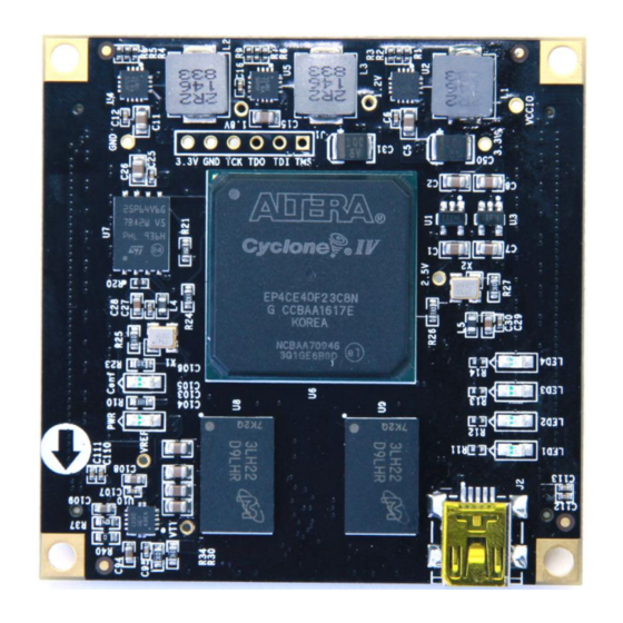
Page 19: Part 9: Structure Diagram
ALINX ALTERA Core Board AC4040 User Manual User LEDs Pin Assignment LED Name FPGA Pin LED0 LED1 LED2 LED3 Part 9: Structure Diagram Figure 9-1: AC4040 FPGA Core board (Top view) 19 / 20 Amazon Store: https://www.amazon.com/alinx... - Page 20 ALINX ALTERA Core Board AC4040 User Manual Figure 9-2: AC4040 FPGA Core board (Top view) 20 / 20 Amazon Store: https://www.amazon.com/alinx...
Need help?
Do you have a question about the ALTERA AC4040 and is the answer not in the manual?
Questions and answers