Table of Contents
Advertisement
Quick Links
Advertisement
Table of Contents

Related Manuals for Alinx KINTEX UltraScale AXKU062


Summary of Contents for Alinx KINTEX UltraScale AXKU062
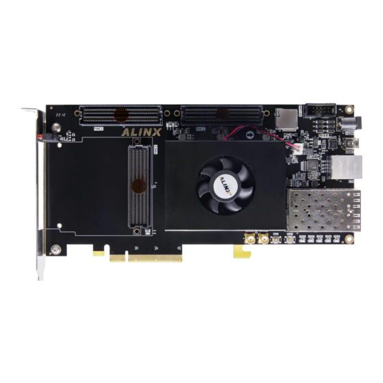
- Page 1 KINTEX UltraScale Development Board AXKU062 User Manual...
-
Page 2: Version Record
KINTEX UltraScale+ FPGA Board AXKU062 User Manual Version Record Version Modify Record REV1.0 Create Documents www.alinx.com 2 / 51... -
Page 3: Table Of Contents
Part 2.9: Temperature Sensor and EEPROM ...............45 Part 2.10: LED Light ......................46 Part 2.11: Keys ........................48 Part 2.12: JTAG Interface ....................49 Part 2.13: Power Supply .....................49 Part 2.14: Fan ......................... 50 Part 2.15:Size Dimension ....................51 http://www.alinx.com.cn 3 / 51 3 / 51... - Page 4 KINTEX UltraScale+ FPGA Board AXKU062 User Manual Alinx Electronic Technology (Shanghai) Co., Ltd, based on KINTEX UltraSacale development platform for the architecture (model: AXKU062) has been officially released. In order to let you quickly understand this development platform, we have compiled this user manual.
- Page 5 1) Two SFP and optical fiber communication interfaces,each fiber optical data communication receives and transmits at speeds of up to 16.3 Gb/s. 2) One PCIE3.0 X8 interfaces , endpoint mode , use to communicate datas http://www.alinx.com.cn 5 / 51 5 / 51...
- Page 6 5) 3 standard FMC expansion port, including 2 LPC FMC expansion ports and 1 HPC FMC expansion port, which can be connected to various FMC modules of Xilinx or Alinx(HDMI input and output modules, binocular camera modules,high-speed AD modules, etc. ) 6) 1 Micro SD card holder, used to store operating system image and file system 2 SMA external interfaces,...
-
Page 7: Part 1 Axku062 Development Board
And IO connection part, the line between the chip and the interface have been done the equal length and differential processing, and the core board size is only 80 * 60 (mm), very suitable for secondary development. http://www.alinx.com.cn 7 / 51 7 / 51... -
Page 8: Part 1.2: Fpga Chip
The main parameters of AXKU062 are as follows: Name Specific parameters Logic Cells 725,550 CLB LUTs 331,680 CLB flip-flops 663,360 Block RAM(Mb) 38.0 DSP Slices 2,760 PCIe Gen3 x8 GTH Transceiver 20 个,16.3Gb/s max Speed Grade Temperature Grade Industrial www.alinx.com 8 / 51... -
Page 9: Part 1.3: Ddr4 Dram
PCB design to ensure high-speed and stable operation of DDR3. The hardware connection mode of FPGA and DDR4 DRAM is shown in Figure 1-3-1: http://www.alinx.com.cn 9 / 51 9 / 51... - Page 10 PL_DDR4_DQ4 IO_L3P_T0L_N4_AD15P_44 AD20 PL_DDR4_DQ5 IO_L6N_T0U_N11_AD6N_44 AG22 PL_DDR4_DQ6 IO_L6P_T0U_N10_AD6P_44 AF22 PL_DDR4_DQ7 IO_L5N_T0U_N9_AD14N_44 AE23 PL_DDR4_DQ8 IO_L8N_T1L_N3_AD5N_44 AF24 PL_DDR4_DQ9 IO_L11P_T1U_N8_GC_44 AJ23 PL_DDR4_DQ10 IO_L8P_T1L_N2_AD5P_44 AF23 PL_DDR4_DQ11 IO_L12N_T1U_N11_GC_44 AH23 PL_DDR4_DQ12 IO_L9N_T1L_N5_AD12N_44 AG25 PL_DDR4_DQ13 IO_L11N_T1U_N9_GC_44 AJ24 PL_DDR4_DQ14 IO_L9P_T1L_N4_AD12P_44 AG24 PL_DDR4_DQ15 IO_L12P_T1U_N10_GC_44 AH22 www.alinx.com 10 / 51...
- Page 11 PL_DDR4_DQ40 IO_L9N_T1L_N5_AD12N_46 AN28 PL_DDR4_DQ41 IO_L12N_T1U_N11_GC_46 AM30 PL_DDR4_DQ42 IO_L8P_T1L_N2_AD5P_46 AP28 PL_DDR4_DQ43 IO_L11N_T1U_N9_GC_46 AM29 PL_DDR4_DQ44 IO_L9P_T1L_N4_AD12P_46 AN27 PL_DDR4_DQ45 IO_L12P_T1U_N10_GC_46 AL30 PL_DDR4_DQ46 IO_L11P_T1U_N8_GC_46 AL29 PL_DDR4_DQ47 IO_L8N_T1L_N3_AD5N_46 AP29 PL_DDR4_DQ48 IO_L14P_T2L_N2_GC_46 AK31 PL_DDR4_DQ49 IO_L18P_T2U_N10_AD2P_46 AH34 PL_DDR4_DQ50 IO_L14N_T2L_N3_GC_46 AK32 http://www.alinx.com.cn 11 / 51 11 / 51...
- Page 12 PL_DDR4_DQS1_P IO_L10P_T1U_N6_QBC_AD4P_44 AH24 PL_DDR4_DQS1_N IO_L10N_T1U_N7_QBC_AD4N_44 AJ25 PL_DDR4_DQS2_P IO_L16P_T2U_N6_QBC_AD3P_44 AJ20 PL_DDR4_DQS2_N IO_L16N_T2U_N7_QBC_AD3N_44 AK20 PL_DDR4_DQS3_P IO_L22P_T3U_N6_DBC_AD0P_44 AP20 PL_DDR4_DQS3_N IO_L22N_T3U_N7_DBC_AD0N_44 AP21 PL_DDR4_DQS4_P IO_L4P_T0U_N6_DBC_AD7P_46 AL27 PL_DDR4_DQS4_N IO_L4N_T0U_N7_DBC_AD7N_46 AL28 PL_DDR4_DQS5_P IO_L10P_T1U_N6_QBC_AD4P_46 AN29 PL_DDR4_DQS5_N IO_L10N_T1U_N7_QBC_AD4N_46 AP30 PL_DDR4_DQS6_P IO_L16P_T2U_N6_QBC_AD3P_46 AH33 PL_DDR4_DQS6_N IO_L16N_T2U_N7_QBC_AD3N_46 AJ33 www.alinx.com 12 / 51...
-
Page 13: Part 1.4: Qspi Flash
IO_L20N_T3L_N3_AD1N_45 AF14 PL_DDR4_RST IO_L15N_T2L_N5_AD11N_45 AG16 Part 1.4: QSPI Flash The AXKU062 FPGA development board is equipped with two 128MBit Quad-SPI FLASH, and the model is N25Q128A, which uses the 3.3V CMOS voltage standard. http://www.alinx.com.cn 13 / 51 13 / 51... - Page 14 Tbale 1-4-2 QSPI Flash Schematic QSPI Flash pin assignments:: Signal Name FPGA FPGA Pin Name QSPI_CCLK CCLK_0 QSPI0_CS_B RDWR_FCS_B_0 QSPI0_IO0 D00_MOSI_0 QSPI0_IO1 D01_DIN_0 QSPI0_IO2 D02_0 QSPI0_IO3 D03_0 Signal Name FPGA FPGA Pin Name QSPI_CCLK CCLK_0 QSPI1_CS_B IO_L2N_T0L_N3_FWE_FCS2_B_65 www.alinx.com 14 / 51...
-
Page 15: Part 1.5: Clock Configuration
(PWR), one is DONE indicator. When the AXKU062 FPGA board is powered on, the power indicator and DONE indicator will light up; when the AXKU062 FPGA is configured, the DONE LED will light up; http://www.alinx.com.cn 15 / 51 15 / 51... -
Page 16: Part 1.7: Power Supply
ETA8156, and an LDO chip SPX3819-1-8 is used to generate the auxiliary power supply of the GTX+1.8V. The VTT and VREF voltages of DDR4 are generated by TPS51200. The power supply design diagram on the board is shown in Figure 1-7-1 below: www.alinx.com 16 / 51... - Page 17 KINTEX UltraScale+ FPGA Board AXKU062 User Manual Figure 1-7-1 Power Supply schematic diagram http://www.alinx.com.cn 17 / 51 17 / 51...
-
Page 18: Part 1.8: Size Dimension
AXK6A2337YG and AXK680337YG. J1 is connected to the IO of BANK66 and BANK68, and the power is 1.8V. Pin assignment of J1 connector J1Pin Signal Name FPGA Pin J1Pin Signal Name FPGA Pin B66_L3_N B66_L1_N B66_L3_P B66_L1_P B66_L7_N B66_L2_N www.alinx.com 18 / 51... - Page 19 B66_L15_N B66_L19_P B66_L15_P B66_L16_N B66_L14_N B66_L16_P B66_L14_P B66_L20_N B66_L18_N B66_L20_P B66_L18_P B66_L22_N B66_L21_N B66_L22_P B66_L21_P B66_L24_N B66_L23_N B66_L24_P B66_L23_P B68_L9_N B68_L19_N B68_L9_P B68_L19_P B68_L8_N B68_L21_N B68_L8_P B68_L21_P B68_L15_N B68_L11_N B68_L15_P B68_L11_P B68_L20_N B68_L23_N http://www.alinx.com.cn 19 / 51 19 / 51...
- Page 20 J2 connector 80 Pin, connect the high speed differential signal of transceiver BANK226~228. Pin assignment of J2 connector Signal Name FPGA Pin Signal Name FPGA Pin 226_TX2_N 226_RX2_N 226_TX2_P 226_RX2_P 226_TX3_N 226_RX3_N 226_TX3_P 226_RX3_P 226_CLK1_N 226_CLK0_N 226_CLK1_P 226_CLK0_P www.alinx.com 20 / 51...
- Page 21 228_CLK0_P 228_CLK1_N 228_CLK0_N J3 is the high-speed difference signal of the transceiver BANK224~226 and the partial signal of BANK64, BANK65 Pin assignment of J3 connector Signal Name FPGA Pin Signal Name FPGA Pin http://www.alinx.com.cn 21 / 51 21 / 51...
- Page 22 B64_L15_P B64_L18_N B64_L16_N AE10 B64_L18_P B64_L16_P AD10 B64_L17_N FPGA_TCK B64_L17_P FPGA_TDO B64_L23_N FPGA_TMS B64_L23_P FPGA_TDI B65_T0U B66_T3U B65_T3U B66_T2U B65_T1U B66_T1U B65_T2U 224_TX0_N 224_RX0_N 224_TX0_P 224_RX0_P 224_TX1_N 224_RX1_N 224_TX1_P 224_RX1_P 224_TX2_N 224_RX2_N 224_TX2_P 224_RX2_P 224_TX3_N 224_RX3_N www.alinx.com 22 / 51...
- Page 23 J4 connects the signal of BANK48 and the partial signal of BANK64. Pin assignment of J4 connector Signal Name FPGA Pin Signal Name FPGA Pin B48_L8_N AG34 B48_T2U AA33 B48_L8_P AF33 B48_T1U AE31 B48_L7_N AG32 B48_T3U B48_L7_P AG31 B47_T3U B48_L10_N AF34 B48_L18_N AD33 http://www.alinx.com.cn 23 / 51 23 / 51...
- Page 24 B48_L2_N AF28 B48_L6_N AG30 B48_L2_P AE28 B48_L6_P AF30 B48_L1_N AF27 B48_L5_N AE30 B48_L1_P AE27 B48_L5_P AD29 B48_L3_N AD28 B48_L16_N AB29 B48_L3_P AC28 B48_L16_P AA29 B48_L14_N AB31 B48_L24_N B48_L14_P AB30 B48_L24_P B48_L20_N B48_L20_P B48_L22_N B48_L22_P B47_T1U B47_T2U www.alinx.com 24 / 51...
- Page 25 J5 connects the signal of BANK47 and the partial signal of BANK65. Pin assignment of J5 connector Signal Name FPGA Pin Signal Name FPGA Pin B65_L10_N B65_L10_P B65_L6_N B65_L23_N B65_L6_P B65_L23_P B65_L19_N B65_L19_P B65_L2_P B65_L9_N B65_L1_N B65_L9_P B65_L1_P B65_L24_N B65_L5_N B65_L24_P B65_L5_P http://www.alinx.com.cn 25 / 51 25 / 51...
- Page 26 B65_L16_P B47_L11_N AA23 B47_L19_N B47_L11_P B47_L19_P B47_L14_N B47_L22_N B47_L14_P B47_L22_P B47_L7_N AB22 B47_L20_N B47_L7_P AA22 B47_L20_P B47_L21_N B47_L17_N B47_L21_P B47_L17_P B47_L3_N AC24 B47_L15_N B47_L3_P AB24 B47_L15_P B47_L23_N B47_L24_N B47_L23_P B47_L24_P B47_L10_N AC21 B47_L13_N B47_L10_P AB21 B47_L13_P www.alinx.com 26 / 51...
- Page 27 Signal Name FPGA Pin +12V +12V +12V +12V +12V +12V +12V +12V +12V +12V B67_L17_N B67_L8_N B67_L17_P B67_L8_P B67_L16_N B67_L6_N B67_L16_P B67_L6_P B67_L15_N B67_L13_N B67_L15_P B67_L13_P B67_L11_N B67_L12_N B67_L11_P B67_L12_P B67_L18_N B67_L4_N B67_L18_P B67_L4_P http://www.alinx.com.cn 27 / 51 27 / 51...
-
Page 28: Part 2: Carrier Board
Through the previous function introduction, you can understand the function of the carrier board part. 2-channel fiber interface 1-channel PCIEx8 interface 1-channel USB Uart interface 1-channel Ethernet RJ45 interface 3-Channel FMC interface www.alinx.com 28 / 51... -
Page 29: Part 2.2: Pcie X8 Interface
The design diagram of the PCIe interface of the AXKU062 FPGA development board is shown in Figure 2-2-1, where the TX transmit signal and the reference clock CLK signal are connected in AC coupled mode. Figure 2-2-1 PCIe card slot schematic diagram http://www.alinx.com.cn 29 / 51 29 / 51... -
Page 30: Part 2.3: Sfp+ Optical Fiber Interface
PCIE channel Reference Clock Negative PCIE_CLK_P MGTREFCLK0P_225 PCIE channel reference Clock Positive PCIE_PERST IO_T3U_N12_PERSTN0_65 PCIE card Reset Signal Part 2.3: SFP+ Optical fiber interface AXKU062 FPGA development board has a two SFP interface. The Users can buy www.alinx.com 30 / 51... - Page 31 SFP light optical LOSS,High level means no light signal is received The 2nd fiber interface FPGA pin assignment is as follows: Signal Name FPGA Pin No. Description SFP2_TX_P SFP Optical Module Data Transmit Positive http://www.alinx.com.cn 31 / 51 31 / 51...
-
Page 32: Part 2.4: Gigabit Ethernet Interface
PHY chip KSZ9031RNX is communicated through RMII bus, and the transmission clock is 25Mhz. Data is sampled on the rising edge and falling samples of the clock. Ethernet PHY chip connection diagram as shown in Figure 2-4-1: www.alinx.com 32 / 51... -
Page 33: Part 2.5: Usb To Serial Port
The conversion chip uses the USB-UAR chip of Silicon Labs CP2102GM. The CP2102 serial chip and the FPGA are connected by a level-shifting chip to adapt to different FPGA BANK http://www.alinx.com.cn 33 / 51 33 / 51... -
Page 34: Part 2.6: Fmc Expansion Port
The AXKU062 FPGA development board comes with two standard FMC LPC expansion ports and one standard FMC HPC expansion ports that can be connected to various FMC modules of XILINX or ALINX (HDMI input and output modules, binocular camera modules, high-speed AD modules, etc.). The LPC FMC1 expansion port has 36 pairs of differential signals, which are respectively connected to the IO of BANK47 and BANK48 of the FPGA chip. - Page 35 FPGA chip BANK227 and BANK228. The schematic diagrams of FPGA and FMC LPC connectors are shown in Figures 2-6-1, 2-6-2 and 2-6-3: Figure 2-6-1 LPC FMC1 schematic diagram Figure 2-6-2 LPC FMC2 schematic diagram http://www.alinx.com.cn 35 / 51 35 / 51...
- Page 36 FMC1_LPC_LA04_P B47_L6_P AB25 FMC reference 4 Data P FMC1_LPC_LA05_N B47_L23_N FMC reference 5 Data N FMC1_LPC_LA05_P B47_L23_P FMC reference 5 Data P FMC1_LPC_LA06_N B47_L1_N FMC reference 6 Data N FMC1_LPC_LA06_P B47_L1_P FMC reference 6 Data P www.alinx.com 36 / 51...
- Page 37 Data P FMC1_LPC_LA26_N B48_L7_N AG32 FMC reference 26 Data N FMC1_LPC_LA26_P B48_L7_P AG31 FMC reference 26 Data P FMC1_LPC_LA27_N B48_L10_N AF34 FMC reference 27 Data N FMC1_LPC_LA27_P B48_L10_P AE33 FMC reference 27 Data P http://www.alinx.com.cn 37 / 51 37 / 51...
- Page 38 Data P FMC2_LPC_LA05_N B65_L4_N FMC reference 5 Data N FMC2_LPC_LA05_P B65_L4_P FMC reference 5 Data P FMC2_LPC_LA06_N B65_L3_N FMC reference 6 Data N FMC2_LPC_LA06_P B65_L3_P FMC reference 6 Data P FMC2_LPC_LA07_N B65_L5_N FMC reference 7 Data N www.alinx.com 38 / 51...
- Page 39 FMC reference 26 Data N FMC2_LPC_LA26_P B64_L21_P AK10 FMC reference 26 Data P FMC2_LPC_LA27_N B64_L24_N FMC reference 27 Data N FMC2_LPC_LA27_P B64_L24_P FMC reference 27 Data P FMC2_LPC_LA28_N B64_L18_N FMC reference 28 Data N http://www.alinx.com.cn 39 / 51 39 / 51...
- Page 40 Data N FMC_HPC_LA08_P B67_L1_P FMC LA 8 Data P FMC_HPC_LA09_N B67_L9_N FMC LA 9 Data N FMC_HPC_LA09_P B67_L9_P FMC LA 9 Data P FMC_HPC_LA10_N B67_L10_N FMC LA 10 Data N FMC_HPC_LA10_P B67_L10_P FMC LA 10 Data P www.alinx.com 40 / 51...
- Page 41 FMC LA 29 Data P FMC_HPC_LA30_N B66_L9_N FMC LA 30 Data N FMC_HPC_LA30_P B66_L9_P FMC LA 30 Data P FMC_HPC_LA31_N B66_L1_N FMC LA 31 Data N FMC_HPC_LA31_P B66_L1_P FMC LA 31 Data P http://www.alinx.com.cn 41 / 51 41 / 51...
- Page 42 FMC HA 16 Data N FMC_HPC_HA16_P B68_L10_P FMC HA 16 Data P FMC_HPC_HA17_CC_N B68_L13_N FMC HA 17 Data(clock)N FMC_HPC_HA17_CC_P B68_L13_P FMC HA 17 Data(clock)P FMC_HPC_HA18_N B68_L21_N FMC HA 18 Data N FMC_HPC_HA18_P B68_L21_P FMC HA 18 Data P www.alinx.com 42 / 51...
- Page 43 Transceiver Data 2 Output FMC_DP2_C2M_N 227_TX2_N Transceiver Data 2 Output FMC_DP3_C2M_P 227_TX3_P Transceiver Data 3 Output FMC_DP3_C2M_N 227_TX3_N Transceiver Data 3 Output FMC_DP4_C2M_P 228_TX1_P Transceiver Data 4 Output FMC_DP4_C2M_N 228_TX1_N Transceiver Data 4 http://www.alinx.com.cn 43 / 51 43 / 51...
-
Page 44: Part 2.7: Sd Card Slot
Clock Signal SD_CMD B64_L19_N AM10 Command Signal SD Data 0 SD_D0 B64_L5_N AL12 SD Data 1 SD_D1 B64_L19_P AL10 SD Data 2 SD_D2 B64_L2_P AN13 SD Data 3 SD_D3 B64_L2_N AP13 SD_CD B64_L22_N card insertion signal www.alinx.com 44 / 51... -
Page 45: Part 2.8: Sma Interface
I2C digital interface. The FPGA reads the temperature near the current FPGA development board through the I2C interface.The model of the EEPROM is 24LC04, and the capacity is: 4Kbit, which is connected to the PS terminal http://www.alinx.com.cn 45 / 51 45 / 51... -
Page 46: Part 2.10: Led Light
LED is configured low level, the user LED lights up. When the connected IO voltage is configured as high level, the user LED will be extinguished. The LEDs hardware connection is shown in Figure 2-10-1: www.alinx.com 46 / 51... - Page 47 KINTEX UltraScale+ FPGA Board AXKU062 User Manual Figure 2-10-1 user LED Figure 2-10-2 panel indicator Figure 2-10-2 panel indicator LED http://www.alinx.com.cn 47 / 51 47 / 51...
-
Page 48: Part 2.11: Keys
The circuit of user key part is shown in Figure 2-11-1. Figure 2-11-1 key connection Keys Pin Assignment: Signal Name FPGA PIN FPGA PIN Description KEY1 B65_T1U User Key Input FPGA_RSETN B65_T2U System Reset www.alinx.com 48 / 51... -
Page 49: Part 2.12: Jtag Interface
The schematic diagram of the power supply design on the board is shown in Figure 2-13-1: http://www.alinx.com.cn 49 / 51 49 / 51... -
Page 50: Part 2.14: Fan
BANK48. If the IO level output is high, the MOSFET is turned on and the fan is working. If the IO level output is low, the fan stops.The fan design on the board is shown in Figure 2-14-1. Figure 2-14-1 www.alinx.com 50 / 51... -
Page 51: Part 2.15:Size Dimension
KINTEX UltraScale+ FPGA Board AXKU062 User Manual Fan Pin Assignment: Signal Name FPGA PIN FPGA Pin No. Description Fan control pin FAN_PWM B64_T0U AK11 Part 2.15:Size Dimension (Top View) http://www.alinx.com.cn 51 / 51 51 / 51...
Need help?
Do you have a question about the KINTEX UltraScale AXKU062 and is the answer not in the manual?
Questions and answers