Table of Contents
Advertisement
Quick Links
Advertisement
Table of Contents

Subscribe to Our Youtube Channel
Related Manuals for Alinx UltraScale+ AXU4EV-P


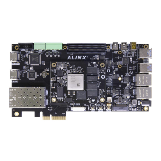
Summary of Contents for Alinx UltraScale+ AXU4EV-P
- Page 1 ZYNQ UltraScale+ FPGA Development Board AXU4EV-P User Manual...
-
Page 2: Version Record
ZYNQ Ultrascale + FPGA Board AXU4EV-P User Manual Version Record Version Date Release By Description Rev 1.0 2021-04-13 Rachel Zhou First Release www.alinx.com 2 / 66... -
Page 3: Table Of Contents
Part 3.8: HDMI Output Interface ............46 Part 3.9: HDMI Input Interface ............48 Part 3.10: SFP Interface ..............50 Part 3.11: PCIe Slot ................52 Part 3.12: CAN Communication Interface ........53 Part 3.13: 485 Communication Interface .......... 54 www.alinx.com 3 / 66... - Page 4 Part 3.19: User LEDs ............... 61 Part 3.20: Keys ................. 62 Part 3.21: DIP Switch Configuration ..........63 Part 3.22: Power Supply ..............64 Part 3.23: ALINX Customized Fan ........... 65 Part 3.24: Carrier Board Size Dimension ......... 66 www.alinx.com 4 / 66...
- Page 5 It is a "professional" ZYNQ development platform. For high-speed data transmission and exchange, pre-verification and post-application of data processing is possible. This product is very suitable for students, engineers and other groups engaged in MPSoCs development. www.alinx.com 5 / 66...
-
Page 6: Part 1: Fpga Development Board Introduction
HDMI Output Interface, 1 HDMI Input Interface, 1 FMC Interface, 2-Channel CAN bus interfaces, 2-Channel RS485 bus interfaces, 1 MIPI Camera Interface and some keys and LEDs. The following figure shows the structure of the entire development system: www.alinx.com 6 / 66... - Page 7 1 PCIEx1 standard M.2 interface, used to connect M.2 SSD solid state drives, with a communication speed of up to 6Gbps. DP Output Interface 1 standard Display Port output display interface, used for video image www.alinx.com 7 / 66...
- Page 8 12.5Gb/s. SD Card Slot Interface 1 Micro SD card holder, used to store operating system image and file system. HDMI Output Interface www.alinx.com 8 / 66...
- Page 9 FMC Expansion Interface 1 standard FMC LPC expansion port, which can be connected to various FMC modules of XILINX or ALINX (HDMI input and output modules, binocular camera modules, high-speed AD modules, etc.). CAN Communication Interface Two-way CAN bus interface, using TI's SN65HVD232 chip, the interface uses 4Pin green terminal blocks.
- Page 10 There are 1 power indicator and 1 DONE Configuration indicator on the core board, 1 power indicator on the carrier board. There are 1 power indicator and 2 user indicators on the carrier board. KEYs 3 KEYs, include 1 Rest KEY and 2 User KEYs. www.alinx.com 10 / 66...
-
Page 11: Part 2: Acu4Ev Core Board
PL side (HP I/O: 96, HD I/O: 84). The wiring between the XCZU4EV chip and the interface has been processed with equal length and differential, and the core board size is only 3.15*2.36 (inch), which is very suitable for secondary development. www.alinx.com 11 / 66... -
Page 12: Part 2.2: Zynq Chip
PCIE Gen2, USB3.0, SATA 3.1, DisplayPort; it also supports USB2.0 , Gigabit Ethernet, SD/SDIO, I2C, CAN, UART, GPIO and other interfaces. The PL end contains a wealth of programmable logic units, DSP and internal RAM. . Figure 2-2-1 detailed the Overall Block Diagram of the ZU4EV Chip. www.alinx.com 12 / 66... - Page 13 Image Video Processor Mali-400 MP2, speed up to 677MHz, 64KB level 2 cache External storage interface, support 32/64bit DDR4/3/3L, LPDDR4/3 interface Static storage interface, support NAND, 2xQuad-SPI FLASH. High-speed connection interface, support PCIe Gen2 x 4, 2 x USB3.0, www.alinx.com 13 / 66...
-
Page 14: Part 2.3: Ddr4 Dram
MT40A512M16LY-062E, of which 4 DDR4 chips are mounted on the PS side to form a 64-bit data bus bandwidth and 4GB capacity. One DDR4 chip is mounted on the PL end, which is a 16-bit data bus width and a capacity www.alinx.com 14 / 66... - Page 15 PCB design to ensure high-speed and stable operation of DDR4. The hardware connection of DDR4 SDRAM on the PS Side is shown in Figure 2-3-1: Figure 2-3-1: DDR3 DRAM schematic diagram www.alinx.com 15 / 66...
- Page 16 Pin Number PS_DDR4_DQS0_P PS_DDR_DQS_P0_504 AF21 PS_DDR4_DQS0_N PS_DDR_DQS_N0_504 AG21 PS_DDR4_DQS1_P PS_DDR_DQS_P1_504 AF23 PS_DDR4_DQS1_N PS_DDR_DQS_N1_504 AG23 PS_DDR4_DQS2_P PS_DDR_DQS_P2_504 AF25 PS_DDR4_DQS2_N PS_DDR_DQS_N2_504 AF26 PS_DDR4_DQS3_P PS_DDR_DQS_P3_504 AE27 PS_DDR4_DQS3_N PS_DDR_DQS_N3_504 AF27 PS_DDR4_DQS4_P PS_DDR_DQS_P4_504 PS_DDR4_DQS4_N PS_DDR_DQS_N4_504 PS_DDR4_DQS5_P PS_DDR_DQS_P5_504 PS_DDR4_DQS5_N PS_DDR_DQS_N5_504 PS_DDR4_DQS6_P PS_DDR_DQS_P6_504 www.alinx.com 16 / 66...
- Page 17 PS_DDR4_DQ19 PS_DDR_DQ19_504 AD24 PS_DDR4_DQ20 PS_DDR_DQ20_504 AG26 PS_DDR4_DQ21 PS_DDR_DQ21_504 AH25 PS_DDR4_DQ22 PS_DDR_DQ22_504 AH26 PS_DDR4_DQ23 PS_DDR_DQ23_504 AG25 PS_DDR4_DQ24 PS_DDR_DQ24_504 AH27 PS_DDR4_DQ25 PS_DDR_DQ25_504 AH28 PS_DDR4_DQ26 PS_DDR_DQ26_504 AF28 PS_DDR4_DQ27 PS_DDR_DQ27_504 AG28 PS_DDR4_DQ28 PS_DDR_DQ28_504 AC27 PS_DDR4_DQ29 PS_DDR_DQ29_504 AD27 PS_DDR4_DQ30 PS_DDR_DQ30_504 AD28 www.alinx.com 17 / 66...
- Page 18 PS_DDR_DQ47_504 PS_DDR4_DQ48 PS_DDR_DQ48_504 PS_DDR4_DQ49 PS_DDR_DQ49_504 PS_DDR4_DQ50 PS_DDR_DQ50_504 PS_DDR4_DQ51 PS_DDR_DQ51_504 PS_DDR4_DQ52 PS_DDR_DQ52_504 PS_DDR4_DQ53 PS_DDR_DQ53_504 PS_DDR4_DQ54 PS_DDR_DQ54_504 PS_DDR4_DQ55 PS_DDR_DQ55_504 PS_DDR4_DQ56 PS_DDR_DQ56_504 PS_DDR4_DQ57 PS_DDR_DQ57_504 PS_DDR4_DQ58 PS_DDR_DQ58_504 PS_DDR4_DQ59 PS_DDR_DQ59_504 PS_DDR4_DQ60 PS_DDR_DQ60_504 PS_DDR4_DQ61 PS_DDR_DQ61_504 PS_DDR4_DQ62 PS_DDR_DQ62_504 PS_DDR4_DQ63 PS_DDR_DQ63_504 PS_DDR4_DM0 PS_DDR_DM0_504 AG20 www.alinx.com 18 / 66...
- Page 19 AA26 PS_DDR4_A12 PS_DDR_A12_504 AB25 PS_DDR4_A13 PS_DDR_A13_504 AB26 PS_DDR4_WE_B PS_DDR_A14_504 AB24 PS_DDR4_CAS_B PS_DDR_A15_504 AC24 PS_DDR4_RAS_B PS_DDR_A16_504 AC23 PS_DDR4_ACT_B PS_DDR_ACT_N_504 PS_DDR4_ALERT_B PS_DDR_ALERT_N_504 PS_DDR4_BA0 PS_DDR_BA0_504 PS_DDR4_BA1 PS_DDR_BA1_504 PS_DDR4_BG0 PS_DDR_BG0_504 PS_DDR4_CS0_B PS_DDR_CS_N0_504 PS_DDR4_ODT0 PS_DDR_ODT0_504 PS_DDR4_PARITY PS_DDR_PARITY_504 PS_DDR4_RESET_B PS_DDR_RST_N_504 PS_DDR4_CLK0_P PS_DDR_CK0_P_504 www.alinx.com 19 / 66...
- Page 20 PL_DDR4_DQ7 IO_L20P_T3L_N2_AD1P_64 PL_DDR4_DQ8 IO_L18N_T2U_N11_AD2N_64 PL_DDR4_DQ9 IO_L18P_T2U_N10_AD2P_64 PL_DDR4_DQ10 IO_L17N_T2U_N9_AD10N_64 PL_DDR4_DQ11 IO_L17P_T2U_N8_AD10P_64 PL_DDR4_DQ12 IO_L15N_T2L_N5_AD11N_64 PL_DDR4_DQ13 IO_L15P_T2L_N4_AD11P_64 PL_DDR4_DQ14 IO_L14N_T2L_N3_GC_64 PL_DDR4_DQ15 IO_L14P_T2L_N2_GC_64 PL_DDR4_DM0 IO_L19P_T3L_N0_DBC_AD9P_64 PL_DDR4_DM1 IO_L13P_T2L_N0_GC_QBC_64 PL_DDR4_A0 IO_L8N_T1L_N3_AD5N_64 PL_DDR4_A1 IO_L3P_T0L_N4_AD15P_64 PL_DDR4_A2 IO_L8P_T1L_N2_AD5P_64 PL_DDR4_A3 IO_L3N_T0L_N5_AD15N_64 PL_DDR4_A4 IO_L11P_T1U_N8_GC_64 PL_DDR4_A5 IO_L4P_T0U_N6_DBC_AD7P_64 PL_DDR4_A6 IO_L9N_T1L_N5_AD12N_64 www.alinx.com 20 / 66...
-
Page 21: Part 2.4: Qspi Flash
FPGA bit files, ARM application code, and other user data files. The specific models and related parameters of QSPI FLASH are shown in Table 2-4-1. Position Model Capacity Factory MT25QU256ABA1EW9 256Mbit Winbond Table 2-4-1: QSPI FLASH Specification www.alinx.com 21 / 66... -
Page 22: Part 2.5: Emmc Flash
FLASH, it can be used as a large-capacity storage device in the ZYNQ system, such as storing ARM applications, system files and other user data files The specific models and www.alinx.com 22 / 66... - Page 23 Figure 2-5-1: QSPI Flash in the schematic Configuration Chip pin assignment: Signal Name Pin Name Pin Number MMC_DAT0 PS_MIO13_500 AH18 MMC_DAT1 PS_MIO14_500 AG18 MMC_DAT2 PS_MIO15_500 AE18 MMC_DAT3 PS_MIO16_500 AF18 MMC_DAT4 PS_MIO17_500 AC18 MMC_DAT5 PS_MIO18_500 AC19 MMC_DAT6 PS_MIO19_500 AE19 www.alinx.com 23 / 66...
-
Page 24: Part 2.6: Clock Configuration
The passive crystal Y2 on the core board provides a 32.768KHz real-time clock source for the PS system. The crystal is connected to the PS_PADI_503 and PS_PADO_503 pins of BANK503 of the ZYNQ chip. The schematic diagram is shown in Figure 2-6-2: www.alinx.com 24 / 66... - Page 25 PS part. The clock input is connected to the PS_REF_CLK_503 pin of BANK503 of the ZYNQ chip. The schematic diagram is shown in Figure 2-6-3: Figure 2-6-3: Active Crystal in PS part Clock pin assignment: Signal Name PS_CLK www.alinx.com 25 / 66...
-
Page 26: Part 2.7: Led
ACU4EV core board. When the core board is powered on, the power indicator will light up; after the FPGA configuration program, the configuration LED light will light up. The LED Schematic in the Core Board is shown in Figure 2-7-1: www.alinx.com 26 / 66... -
Page 27: Part 2.8: Power Supply
The core board uses a PMIC chip TPS6508641 to generate all the power required by the XCZU4EV chip. For the TPS6508641 power supply design, please refer to the power supply chip manual. The design block diagram is as follows: www.alinx.com 27 / 66... - Page 28 ZYNQ Ultrascale + FPGA Board AXU4EV-P User Manual In addition, the VCCIO power supply of BANK65 and BANK66 of XCZU4EV chip is provided by the carrier board, which is convenient for users to modify, but the maximum power supply cannot exceed 1.8V. www.alinx.com 28 / 66...
-
Page 29: Part 2.9: Acu4Ev Core Board Size Dimension
MIO, VCCO_65, VCCO_66 and +12V power supply of PS. Among them, the IO level standard of BANK43~46 is 3.3V, and the level standard of BANK65 and BANK66 is determined by the VCCO_65 and VCCO_66 power supply of the carrier board, but cannot exceed +1.8V; www.alinx.com 29 / 66... - Page 30 B65_L4_P B65_L20_N B65_L1_N B65_L6_N B65_L1_P B65_L6_P B65_L7_P B65_L17_P B65_L7_N B65_L17_N B65_L15_P B65_L9_P B65_L15_N B65_L9_N B65_L16_P B65_L3_N B65_L16_N B65_L3_P B65_L14_P B65_L19_P B65_L14_N B65_L19_N B65_L5_N B65_L18_P B65_L5_P B65_L18_N B65_L11_N B65_L8_P B65_L11_P B65_L8_N B65_L10_N B65_L24_N B65_L10_P B65_L24_P B66_L3_P B65_L12_P www.alinx.com 30 / 66...
- Page 31 B66_L12_P B66_L7_P B66_L12_N B66_L7_N B66_L13_N B66_L10_P B66_L13_P B66_L10_N B66_L8_N B66_L9_P B66_L8_P B66_L9_N Pin assignment of board to board connector J30 J30 Pin Signal Name Pin Number J30 Pin Signal Name Pin Number B66_L14_P FPGA_TDI B66_L14_N FPGA_TCK www.alinx.com 31 / 66...
- Page 32 B66_L23_N B25_L9_P B66_L23_P B25_L9_N B25_L5_N B25_L10_P B25_L5_P B25_L10_N B66_L18_N B25_L12_P B66_L18_P B25_L12_N B25_L4_N B25_L11_P B25_L4_P B25_L11_N B26_L11_P B25_L6_N B26_L11_N B25_L6_P B26_L10_N B26_L6_N B26_L10_P B26_L6_P B26_L7_N B26_L3_N B26_L7_P B26_L3_P B26_L9_N B26_L2_N B26_L9_P B26_L2_P B26_L5_N B26_L4_N B26_L5_P B26_L4_P www.alinx.com 32 / 66...
- Page 33 J31 Pin Signal Name Pin Number B24_L10_P B24_L7_P AA13 B24_L10_N B24_L7_N AB13 B24_L6_P AC14 B44_L6_P AC12 B24_L6_N AC13 B44_L6_N AD12 B24_L5_P AD15 B44_L7_P AD11 B24_L5_N AD14 B44_L7_N AD10 B24_L1_P AE15 B44_L8_N AC11 B24_L1_N AE14 B44_L8_P AB11 www.alinx.com 33 / 66...
- Page 34 B24_L11_N B44_L1_N AH10 B24_L11_P B44_L1_P AG10 B24_L9_N B24_L4_P AE13 B24_L9_P B24_L4_N AF13 B24_L8_P AB15 B44_L5_P AE12 B24_L8_N AB14 B44_L5_N AF12 B44_L2_N AG11 B44_L4_N AF10 B44_L2_P AF11 B44_L4_P AE10 VBAT_IN B44_L11_P B44_L11_N PS_POR_B 224_CLK0_P 224_CLK1_P 224_CLK0_N 224_CLK1_N www.alinx.com 34 / 66...
- Page 35 Pin assignment of board to board connector J32 J32 Pin Signal Name Pin Number J32 Pin Signal Name Pin Number PS_MIO35 PS_MIO30 PS_MIO29 PS_MIO31 PS_MIO58 PS_MIO53 PS_MODE0 PS_MIO52 PS_MODE1 PS_MIO55 PS_MODE2 PS_MIO56 PS_MODE3 PS_MIO57 PS_MIO36 PS_MIO54 PS_MIO37 PS_MIO27 PS_MIO28 PS_MIO77 PS_MIO59 PS_MIO76 PS_MIO60 www.alinx.com 35 / 66...
- Page 36 PS_MIO68 PS_MIO47 PS_MIO64 PS_MIO48 PS_MIO69 PS_MIO41 PS_MIO74 PS_MIO32 PS_MIO73 PS_MIO46 PS_MIO72 PS_MIO50 PS_MIO71 PS_MIO49 PS_MIO75 PS_MIO34 PS_MIO70 PS_MIO26 PS_MIO43 PS_MIO24 AB19 PS_MIO51 PS_MIO25 AB21 PS_MIO42 PS_MIO33 VCCO_65 VCCO_66 VCCO_65 VCCO_66 VCCO_65 VCCO_66 +12V +12V +12V +12V www.alinx.com 36 / 66...
- Page 37 ZYNQ Ultrascale + FPGA Board AXU4EV-P User Manual +12V +12V +12V +12V +12V +12V +12V +12V +12V +12V www.alinx.com 37 / 66...
-
Page 38: Part 3: Carrier Board
M.2 interface for connecting M.2 SSD solid state drives, with a communication speed of up to 6Gbps. The M.2 interface uses the M key slot, which only supports PCI-E, not SATA. When users choose SSD solid state drives, they www.alinx.com 38 / 66... -
Page 39: Part 3.3: Dp Interface
PCIE Reference Clock Positive 505_PCIE_REFCLK_N 505_CLK0_N PCIE Reference Clock Negative PCIE_RSTn_MIO37 PS_MIO37_501 PCIE Reset Signal Part 3.3: DP Interface The AXU4EV-P development board has a standard DisplayPort output display interface for video image display. The interface supports VESA www.alinx.com 39 / 66... - Page 40 Low bits of DP Data GT0_DP_TX_P 505_TX3_P Transmit Positive Low bits of DP Data GT0_DP_TX_N 505_TX3_N Transmit Negative High bits of DP Data GT1_DP_TX_P 505_TX2_P Transmit Positive High bits of DP Data GT1_DP_TX_N 505_TX2_N Transmit Negative www.alinx.com 40 / 66...
-
Page 41: Part 3.4: Usb3.0 Interface
USB3.0 connection is shown as 3-4-1: USB__CLK USB__STP DP/DM USB__NXT BANK USB PHY USB__DIR (USB3320C) USB3.0 HUB ZYNQ (GL3523T) USB_DATA0~USB_DATA7 Ultra USB_RESET_N Scale+ USB_SSTXP USB_TXP_UP USB_SSTXN USB_TXN_UP BANK USB_SSRXP USB_RXP_UP USB_SSRXN USB_RXN_UP 26Mhz Si5332 USB3.0参考时钟 Figure 3-4-1: USB3.0 Interface Schematic www.alinx.com 41 / 66... -
Page 42: Part 3.5: Gigabit Ethernet Interface
MDIO bus for PHY register management. When the KSZ9031RNX is powered on, it will detect the level status of some specific IOs to determine its own operating mode. Table 3-5-1 describes the default settings after the GPHY chip is powered on. www.alinx.com 42 / 66... - Page 43 25Mhz. Data is sampled on the rising edge and falling samples of the clock. RGMII TX GPHY BANK (KSZ9031RNX) RGMII RX ZYNQ Ultra Scale+ RGMII TX GPHY BANK (KSZ9031RNX) RGMII RX Figure 3-5-1: ZYNQ PS system and GPHY connection diagram www.alinx.com 43 / 66...
-
Page 44: Part 3.6: Usb To Serial Port
Ethernet 2 MDIO Clock Management PHY2_MDIO B66_L22_P Ethernet 2 MDIO Management Data PHY2_RESET B66_L14_N Ethernet 2 Reset Signal Part 3.6: USB to Serial Port The AXU4EV-P carrier board is equipped with two Uart to USB ports, one www.alinx.com 44 / 66... -
Page 45: Part 3.7: Sd Card Slot Interface
PL Uart Data Output PL_UART_RX B43_L9_N AH10 PL Uart Data Input Part 3.7: SD Card Slot Interface The AXU4EV-P FPGA Development Board contains a Micro SD card interface to provide user access to the SD card memory, the BOOT www.alinx.com 45 / 66... -
Page 46: Part 3.8: Hdmi Output Interface
SD Data3 SD_CD PS_MIO45 SD card insertion signal Part 3.8: HDMI Output Interface The HDMI output interface uses the ADV7511 HDMI (DVI) encoding chip from ANALOG DEVICE, which supports up to 1080P@60Hz output and 3D output. www.alinx.com 46 / 66... - Page 47 HDMI_DE B35_L9_P HDMI Video Signal Enable HDMI_D0 B35_L9_N HDMI Video Signal Data0 HDMI_D1 B35_L22_N HDMI Video Signal Data1 HDMI_D2 B35_L22_P HDMI Video Signal Data2 HDMI_D3 B35_L20_N HDMI Video Signal Data3 HDMI_D4 B35_L20_P HDMI Video Signal Data4 www.alinx.com 47 / 66...
-
Page 48: Part 3.9: Hdmi Input Interface
The IIC configuration interface of ADV7611 is also connected to the IO of ZU4EV PL. ZYNQ initializes and controls ADV7611 through I2C bus programming. The hardware schematic of the HDMI input interface is shown in Figure 3-9-1. www.alinx.com 48 / 66... - Page 49 HDMI Input Video Signal Data3 HDMI_IN_D3 B43_L6_P AC12 HDMI Input Video Signal Data4 HDMI_IN_D4 B44_L6_P AC14 HDMI Input Video Signal Data5 HDMI_IN_D5 B44_L6_N AC13 HDMI Input Video Signal Data6 HDMI_IN_D6 B43_L6_N AD12 HDMI Input Video Signal Data7 www.alinx.com 49 / 66...
-
Page 50: Part 3.10: Sfp Interface
GNK transceiver of ZYNQ BANK224, and the data rate of each TX transmission and RX reception is up to 12.5Gb/s. The reference clock of the GTH transceiver is provided by the 125M differential clock of the core board. The SFP Schematic detailed is shown in Figure 3-10-1: www.alinx.com 50 / 66... - Page 51 224_RX1_P Optical Module 2 Data Receive Positive Optical Module Light Emission Prohibited, High SFP_TX_DIS B45_L12_P Level (Positive) Enable Optical Module 1 Receive LOSS SFP1_LOSS B45_L9_N Detect Signal Optical Module 2 Receive LOSS SFP2_LOSS B45_L9_P Detect Signal www.alinx.com 51 / 66...
-
Page 52: Part 3.11: Pcie Slot
Figure 3-11: PCIe Interface Schematic PCIe x2 Interface ZYNQ Pin Assignment Signal Name ZYNQ Pin Name ZYNQ Pin Description Number PCIE_RX0_N 224_RX2_N PCIE Channel 0 Data Receive Negative PCIE_RX0_P 224_RX2_P PCIE Channel 0 Data Receive Positive www.alinx.com 52 / 66... -
Page 53: Part 3.12: Can Communication Interface
Figure 3-12-1: Connection diagram of CAN transceiver chip on PS side The CAN communication pin assignments are as follows: Signal Name ZYNQ Pin Name ZYNQ Pin Number Description PS_CAN1_TX PS_MIO32 CAN1 Transmitter PS_CAN1_RX PS_MIO33 CAN1 Receiver www.alinx.com 53 / 66... -
Page 54: Part 3.13: 485 Communication Interface
The 1 Channel 485 Receiver PL_485_DE1 B45_L10_N The 1 Channel 485 Transmit Enable PL_485_TXD2 B43_L3_N AH11 The 2 Channel 485 Transceiver PL_485_RXD2 B43_L3_P AH12 The 2 Channel 485 Receiver PL_485_DE2 B45_L10_P The 2 Channel 485 Transmit Enable www.alinx.com 54 / 66... -
Page 55: Part 3.14: Mipi Camera Interface
Part 3.14: MIPI Camera Interface The AXU4EV-P carrier board includes a MIPI camera interface, which can be used to connect with the ALINX Brand MIPI OV5640 camera module AN5641. MIPI interface 15PIN FPC connector, 2 LANE data and 1 pair of clock, connected to the differential IO pin of BANK65, the level standard is 1.2V... -
Page 56: Part 3.15: Fmc Interface
Part 3.15: FMC Interface The AXU4EV-P FPGA Carrier board has a standard FMC HPC expansion port that can be connected to various FMC modules of XILINX or ALINX (HDMI input and output modules, binocular camera modules, high-speed AD modules, etc.). The FMC expansion port contains 36 pairs of differential IO signals. - Page 57 Data N FMC_LA10_P B65_L6_P FMC Reference 10 Data P FMC_LA10_N B65_L6_N FMC Reference 10 Data N FMC_LA11_P B65_L5_P FMC Reference 11 Data P FMC_LA11_N B65_L5_N FMC Reference 11 Data N FMC_LA12_P B65_L9_P FMC Reference 12 Data P www.alinx.com 57 / 66...
- Page 58 Data N FMC_LA28_P B66_L10_P FMC Reference 28 Data P FMC_LA28_N B66_L10_N FMC Reference 28 Data N FMC_LA29_P B66_L7_P FMC Reference 29 Data P FMC_LA29_N B66_L7_N FMC Reference 29 Data N FMC_LA30_P B66_L13_P FMC Reference 30 Data P www.alinx.com 58 / 66...
-
Page 59: Part 3.16: Jtag Debug Port
JTAG signal to ensure that the signal voltage is within the range accepted by the FPGA and avoid damage to the ZYNQ UltraScale+ chip. Figure 3-16-1: JTAG Interface Schematic www.alinx.com 59 / 66... -
Page 60: Part 3.17: Real-Time Clock
EEPROM is 24LC04, and the capacity is: 4Kbit (2 * 256 * 8bit), which is connected to the PS terminal through the I2C bus. A high-precision, low-power, digital temperature sensor chip is installed on the AXU4EV-P FPGA development board, and the model is LM75 from ON www.alinx.com 60 / 66... -
Page 61: Part 3.19: User Leds
When the IO voltage of the connected user LED light is low, the user LED light is off, and when the connected IO voltage is high, the user LED will be lit. The schematic diagram of the user's LED light hardware connection is shown in Figure 3-19-1: www.alinx.com 61 / 66... -
Page 62: Part 3.20: Keys
One user KEY is connected to the MIO of the PS, and one is connected to the IO of the PL. The reset KEY and the user KEYs are both low-level active. The connection diagram of the user key is shown in Figure 3-20-1: www.alinx.com 62 / 66... -
Page 63: Part 3.21: Dip Switch Configuration
The user can select different startup modes through the DIP switch SW1 on the expansion board. The SW1 startup mode configuration is shown in the following table 3-21-1. Dial Position (1, 2, 3, 4) MODE[3:0] Start mode 0000 PS JTAG ON,ON,ON,ON www.alinx.com 63 / 66... -
Page 64: Part 3.22: Power Supply
Figure 3-22-1: +12V 2A +5.0V/6A TPS54620 12V电源 +1.2V +3.3V/2A MP1482 +1.8V/2A MP1482 Figure 3-22-1: Carrier Board Power Schematic The functions of each power distribution are shown in the following table: www.alinx.com 64 / 66... -
Page 65: Part 3.23: Alinx Customized Fan
Ethernet, USB2.0, SD, DP, CAN, RS485 +1.2V BANK65 of Core Board Part 3.23: ALINX Customized Fan Because AXU4EV-P generates a lot of heat when it works normally, we add a heat sink and fan to the chip on the board to prevent the chip from overheating. -
Page 66: Part 3.24: Carrier Board Size Dimension
ZYNQ Ultrascale + FPGA Board AXU4EV-P User Manual Part 3.24: Carrier Board Size Dimension Figure 3-24-1: Top View www.alinx.com 66 / 66...
Need help?
Do you have a question about the UltraScale+ AXU4EV-P and is the answer not in the manual?
Questions and answers