Table of Contents
Advertisement
Quick Links
Advertisement
Table of Contents

Subscribe to Our Youtube Channel
Related Manuals for Alinx AXU15EGB


Summary of Contents for Alinx AXU15EGB
- Page 1 ZYNQ UltraScale+ FPGA Development Board AXU15EGB User Manual...
-
Page 2: Version Record
AXU15EGB User Manual Version Record Version Date Release By Description Rev 1.1 2021-06-24 Rachel Zhou First Release 2 / 66 www.alinx.com... -
Page 3: Table Of Contents
AXU15EGB User Manual Table of Contents Version Record .....................2 Part 1: FPGA Development Board Introduction .......... 7 Part 2: ACU15EG Core Board ..............12 Part 2.1: ACU15EG Core Board Introduction ........12 Part 2.2: ZYNQ Chip ................13 Part 2.3: DDR4 DRAM ................15 Part 2.4: QSPI Flash ................22... - Page 4 Part 3.16: EEPROM and Temperature Sensor ........60 Part 3.17: User LEDs ................61 Part 3.18: Keys ................... 62 Part 3.19: DIP Switch Configuration ...........63 Part 3.20: Power Supply ..............64 Part 3.21: ALINX Customized Fan ............. 65 Part 3.22: Carrier Board Size Dimension ...........66 4 / 66 www.alinx.com...
- Page 5 AXU15EGB User Manual This MPSoCs FPGA development platform adopts the core board + carrier board mode, which is convenient for users to use the core board for secondary development. The core board uses XILINX Zynq UltraScale+ EG chip ZU15EG solution, uses Processing System(PS)+Programmable Logic(PL) technology to integrate dual-core ARM ARM Cortex-A53 and FPGA programmable logic on a single chip.
- Page 6 AXU15EGB User Manual 6 / 66 www.alinx.com...
-
Page 7: Part 1: Fpga Development Board Introduction
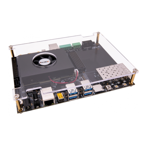
AXU15EGB User Manual Part 1: FPGA Development Board Introduction The entire structure of the AXU15EGB PGA development board is inherited from our consistent core board + carrier board model. A high-speed inter-board connector is used between the core board and the carrier board. - Page 8 AXU15EGB User Manual Figure 1-1-1: The Schematic Diagram of the AXU15EGB Through this diagram, you can see the interfaces and functions that the AXU15EGB FPGA Development Board contains: ZU15EG core board It consists of ZU15EG +4GB DDR4 (PS) +2GB DDR4 (PL) +8GB eMMC FLASH + 512Mb QSPI FLASH, and there are 2 crystal oscillators to provide the clock, a single-ended 33.3333MHz crystal oscillator for the...
- Page 9 FMC Expansion Interface 1 standard FMC LPC expansion port, which can be connected to various FMC modules of XILINX or ALINX (HDMI input and output modules, binocular camera modules, high-speed AD modules, etc.). CAN Communication Interface 9 / 66...
- Page 10 2 Lane MIPI camera input interfaces, used to connect MIPI camera module (AN5641). 40-pin Expansion Header The 40-pin 2.54mm pitch expansion port use for external ALINX modules (binocular camera, TFT LCD screen, high-speed AD module, etc.). The expansion port includes 1 channel of 5V power supply, 2 channels of 3.3V power supply, 3 channels of ground, and 34 channels...
- Page 11 AXU15EGB User Manual indicator,1 DONE Configuration indicator and 2 user indicators on the carrier board. KEYs 3 KEYs, include 1 Rest KEY and 2 User KEYs. 11 / 66 www.alinx.com...
-
Page 12: Part 2: Acu15Eg Core Board
AXU15EGB User Manual Part 2: ACU15EG Core Board Part 2.1: ACU15EG Core Board Introduction ACU15EG (core board model, the same below) FPGA core board, ZYNQ chip is based on XCZU15EG-2FFVB1156I of XILINX company Zynq UltraScale+ MPSoCs EG Family. This core board uses 6 Micron DDR4 chips MT40A512M16GE, of which 4 DDR4 chips are mounted on the PS side to form a 64-bit data bus bandwidth and 4GB capacity. -
Page 13: Part 2.2: Zynq Chip
AXU15EGB User Manual Figure 2-1-1: ACU15EG Core Board (Front View) Part 2.2: ZYNQ Chip The FPGA core board ACU15EG uses Xilinx's Zynq UltraScale+ MPSoCs EG family chip, module XCZU15EG-2FFVB1156I. The PS system of the ZU15EG chip integrates 4 ARM Cortex™-A53 processors with a speed of up to 1.3Ghz and supports Level 2 Cache;... - Page 14 AXU15EGB User Manual Figure 2-2-1: Overall Block Diagram of the ZYNQ ZU15EG Chip The main parameters of the PS system part are as follows: ARM quad-core Cortex ™ -A53 processor, speed up to 1.3GHz, each CPU 32KB level 1 instruction and data cache, 1MB level 2 cache, shared by 2 CPUs ...
-
Page 15: Part 2.3: Ddr4 Dram
AXU15EGB User Manual Common connection interfaces: 2 x USB2.0, 2 x SD/SDIO, 2 x UART, 2 x CAN 2.0B, 2 x I2C, 2 x SPI, 4 x 32b GPIO Power management: Support the four-part division of power supply Full/Low/PL/Battery ... - Page 16 AXU15EGB User Manual highest operating speed of the DDR4 SDRAM on the PL side can reach 1200MHz (data rate 2400Mbps), and two piece of DDR4 is connected to the BANK64,65 interface of the FPGA. The specific configuration of DDR4 SDRAM...
- Page 17 AXU15EGB User Manual Figure 2-3-2: DDR4 DRAM schematic diagram PS Side DDR4 DRAM pin assignment: Signal Name Pin Name Pin Number PS_DDR4_DQS0_N PS_DDR_DQS_N0_504 AN19 PS_DDR4_DQS0_P PS_DDR_DQS_P0_504 AN18 PS_DDR4_DQS1_N PS_DDR_DQS_N1_504 AN22 PS_DDR4_DQS1_P PS_DDR_DQS_P1_504 AN21 PS_DDR4_DQS2_N PS_DDR_DQS_N2_504 AJ19 PS_DDR4_DQS2_P PS_DDR_DQS_P2_504 AH19 PS_DDR4_DQS3_N...
- Page 18 AXU15EGB User Manual PS_DDR4_DQ2 PS_DDR_DQ2_504 AP19 PS_DDR4_DQ3 PS_DDR_DQ3_504 AP17 PS_DDR4_DQ4 PS_DDR_DQ4_504 AM20 PS_DDR4_DQ5 PS_DDR_DQ5_504 AM19 PS_DDR4_DQ6 PS_DDR_DQ6_504 AM18 PS_DDR4_DQ7 PS_DDR_DQ7_504 AL18 PS_DDR4_DQ8 PS_DDR_DQ8_504 AP22 PS_DDR4_DQ9 PS_DDR_DQ9_504 AP21 PS_DDR4_DQ10 PS_DDR_DQ10_504 AP24 PS_DDR4_DQ11 PS_DDR_DQ11_504 AN23 PS_DDR4_DQ12 PS_DDR_DQ12_504 AL21 PS_DDR4_DQ13 PS_DDR_DQ13_504 AL22 PS_DDR4_DQ14...
- Page 19 AXU15EGB User Manual PS_DDR4_DQ38 PS_DDR_DQ38_504 AK30 PS_DDR4_DQ39 PS_DDR_DQ39_504 AJ29 PS_DDR4_DQ40 PS_DDR_DQ40_504 AE27 PS_DDR4_DQ41 PS_DDR_DQ41_504 AF28 PS_DDR4_DQ42 PS_DDR_DQ42_504 AF30 PS_DDR4_DQ43 PS_DDR_DQ43_504 AF31 PS_DDR4_DQ44 PS_DDR_DQ44_504 AD28 PS_DDR4_DQ45 PS_DDR_DQ45_504 AD27 PS_DDR4_DQ46 PS_DDR_DQ46_504 AD29 PS_DDR4_DQ47 PS_DDR_DQ47_504 AD30 PS_DDR4_DQ48 PS_DDR_DQ48_504 AH33 PS_DDR4_DQ49 PS_DDR_DQ49_504 AJ34 PS_DDR4_DQ50...
- Page 20 AXU15EGB User Manual PS_DDR4_A2 PS_DDR_A2_504 AP26 PS_DDR4_A3 PS_DDR_A3_504 AP27 PS_DDR4_A4 PS_DDR_A4_504 AP25 PS_DDR4_A5 PS_DDR_A5_504 AN24 PS_DDR4_A6 PS_DDR_A6_504 AM29 PS_DDR4_A7 PS_DDR_A7_504 AM28 PS_DDR4_A8 PS_DDR_A8_504 AM26 PS_DDR4_A9 PS_DDR_A9_504 AM25 PS_DDR4_A10 PS_DDR_A10_504 AL28 PS_DDR4_A11 PS_DDR_A11_504 AK27 PS_DDR4_A12 PS_DDR_A12_504 AJ25 PS_DDR4_A13 PS_DDR_A13_504 AL25 PS_DDR4_WE_B...
- Page 21 AXU15EGB User Manual PL_DDR4_DQS2_P IO_L10P_T1U_N6_QBC_AD4P_65 PL_DDR4_DQS3_N IO_L4N_T0U_N7_DBC_AD7N_65 PL_DDR4_DQS3_P IO_L4P_T0U_N6_DBC_AD7P_65 AG11 PL_DDR4_DQ0 IO_L24P_T3U_N10 _I2C_SDA_65 PL_DDR4_DQ1 IO_L20P_T3L_N2_AD1P_65 PL_DDR4_DQ2 IO_L23N_T3U_N9_65 PL_DDR4_DQ3 IO_L21P_T3L_N4_AD8P_65 PL_DDR4_DQ4 IO_L23P_T3U_N8_I2C_SCLK_65 PL_DDR4_DQ5 IO_L20N_T3L_N3_AD1N_65 PL_DDR4_DQ6 IO_L24N_T3U_N11_PERSTN0_65 PL_DDR4_DQ7 IO_L21N_T3L_N5_AD8N_65 PL_DDR4_DQ8 IO_L17P_T2U_N8_AD10P_65 PL_DDR4_DQ9 IO_L15P_T2L_N4_AD11P_65 PL_DDR4_DQ10 IO_L18P_T2U_N10_AD2P_65 PL_DDR4_DQ11 IO_L14N_T2L_N3_GC_65 PL_DDR4_DQ12 IO_L18N_T2U_N11_AD2N_65 PL_DDR4_DQ13 IO_L14P_T2L_N2_GC_65 PL_DDR4_DQ14...
-
Page 22: Part 2.4: Qspi Flash
AXU15EGB User Manual PL_DDR4_DM1 IO_L13P_T2L_N0_GC_QBC_65 PL_DDR4_DM2 IO_L7P_T1L_N0_QBC_AD13P_65 PL_DDR4_DM3 IO_L1P_T0L_N0_DBC_65 AE10 PL_DDR4_A0 IO_L5P_T0U_N8_AD14P_64 PL_DDR4_A1 IO_L16P_T2U_N6_QBC_AD3P_64 PL_DDR4_A2 IO_L10P_T1U_N6_QBC_AD4P_64 PL_DDR4_A3 IO_L15P_T2L_N4_AD11P_64 PL_DDR4_A4 IO_L11P_T1U_N8_GC_64 PL_DDR4_A5 IO_L10N_T1U_N7_QBC_AD4N_64 PL_DDR4_A6 IO_L3N_T0L_N5_AD15N_64 AM10 PL_DDR4_A7 IO_L7P_T1L_N0_QBC_AD13P_64 PL_DDR4_A8 IO_L11N_T1U_N9_GC_64 PL_DDR4_A9 IO_L4N_T0U_N7_DBC_AD7N_64 AP10 PL_DDR4_A10 IO_L14P_T2L_N2_GC_64 PL_DDR4_A11 IO_L8N_T1L_N3_AD5N_64 PL_DDR4_A12 IO_L15N_T2L_N5_AD11N_64 PL_DDR4_A13 IO_L7N_T1L_N1_QBC_AD13N_64... - Page 23 AXU15EGB User Manual the non-volatile nature of QSPI FLASH, it can be used as a boot device for the system to store the boot image of the system. These images mainly include FPGA bit files, ARM application code, and other user data files. The specific models and related parameters of QSPI FLASH are shown in Table 2-4-1.
-
Page 24: Part 2.5: Emmc Flash
AXU15EGB User Manual MIO0_QSPI0_SCLK PS_MIO0_500 AF16 MIO1_QSPI0_IO1 PS_MIO1_500 AJ16 MIO1_QSPI0_IO2 PS_MIO2_500 AD16 MIO1_QSPI0_IO3 PS_MIO3_500 AG16 MIO1_QSPI0_IO0 PS_MIO4_500 AH16 MIO7_QSPI1_SS_B PS_MIO7_500 AD17 MIO12_QSPI1_SCLK PS_MIO12_500 AJ17 MIO8_QSPI1_IO0 PS_MIO8_500 AE17 MIO8_QSPI1_IO1 PS_MIO9_500 AP15 MIO8_QSPI1_IO2 PS_MIO10_500 AH17 MIO8_QSPI1_IO3 PS_MIO11_500 AF17 Part 2.5: eMMC Flash... -
Page 25: Part 2.6: Clock Configuration
AXU15EGB User Manual Figure 2-5-1: eMMC Flash in the schematic Configuration Chip pin assignment: Signal Name Pin Name Pin Number MMC_CCLK PS_MIO22_500 AD20 MMC_CMD PS_MIO21_500 AF18 MMC_DAT0 PS_MIO13_500 AK17 MMC_DAT1 PS_MIO14_500 AL16 MMC_DAT2 PS_MIO15_500 AN16 MMC_DAT3 PS_MIO16_500 AM16 MMC_DAT4 PS_MIO17_500... - Page 26 AXU15EGB User Manual Figure 2-6-1: Core Board Clock Source PS System RTC Real Time Clock The passive crystal Y1 on the core board provides a 32.768KHz real-time clock source for the PS system. The crystal is connected to the PS_PADI_503 and PS_PADO_503 pins of BANK503 of the ZYNQ chip.
- Page 27 AXU15EGB User Manual PS System Clock Source The X1 crystal on the core board provides a 33.333MHz clock input for the PS part. The clock input is connected to the PS_REF_CLK_503 pin of BANK503 of the ZYNQ chip. The schematic diagram is shown in Figure 2-6-3:...
-
Page 28: Part 2.7: Power Supply
AXU15EGB User Manual Figure 2-6-4: PL system clock source Clock pin assignment: Signal Name PL_CLK0_P PL_CLK0_N Part 2.7: Power Supply The power supply voltage of the ACU15EG core board is DC12V, which is supplied by connecting the carrier board. The core board uses 2 MYMGM1R824 power chips in parallel to achieve a 50A current to provide the core power of the XCZU15EG with 0.85V. - Page 29 AXU15EGB User Manual 29 / 66 www.alinx.com...
-
Page 30: Part 2.8: Acu15Eg Core Board Size Dimension
AXU15EGB User Manual Part 2.8: ACU15EG Core Board Size Dimension Figure 2-8-1: ACU15EG Core Board Size Dimension Part 2.10: Board to Board Connectors pin assignment The core board has a total of four high-speed expansion ports. It uses four 120-pin inter-board connectors (J29/J30/J31/J32) to connect to the carrier board. - Page 31 AXU15EGB User Manual J29 Pin Signal Name J29 Pin Signal Name Pin Number Number B66_L3_P AA11 B67_L1_P B66_L3_N AA10 B67_L1_N B66_L2_P AB11 B66_L7_P B66_L2_N AB10 B66_L7_N B66_L5_N AA12 B66_L8_P B66_L5_P B66_L8_N B67_L2_N B66_L1_N AC11 B67_L2_P B66_L1_P AC12 B66_L19_P B66_L11_N B66_L19_N...
- Page 32 AXU15EGB User Manual B67_L23_P B67_L17_N B67_L7_N B67_L13_P B67_L7_P B67_L13_N B67_L9_P B66_L23_N B67_L9_N B66_L23_P B67_L18_P B67_L12_P B67_L18_N B67_L12_N B67_L10_P B67_L14_P B67_L10_N B67_L14_N 228_RX1_N 228_RX0_N 228_RX1_P 228_RX0_P 228_TX1_N 228_TX0_N 228_TX1_P 228_TX0_P 228_RX3_N 228_RX2_N 228_RX3_P 228_RX2_P 228_TX3_N 228_TX2_N 228_TX3_P 228_TX2_P 228_CLK0_N 228_CLK1_N 228_CLK0_P...
- Page 33 AXU15EGB User Manual 505_RX0_P AB33 505_TX3_P 505_RX0_N AB34 505_TX3_N 505_CLK1_P 505_TX2_P 505_CLK1_N 505_TX2_N 505_RX2_N 505_CLK2_P 505_RX2_P 505_CLK2_N 505_RX3_P 505_RX1_N AA32 505_RX3_N 505_RX1_P AA31 505_CLK3_P 505_TX1_N 505_CLK3_N 505_TX1_P PS_MIO26 USB_STP PS_MIO35 USB_DIR PS_MIO28 USB_CLK PS_MIO37 USB_NXT PS_MIO39 USB_DATA0 PS_MIO27 USB_DATA1 PS_MIO40...
- Page 34 AXU15EGB User Manual PS_MIO41 PHY1_TXD3 PS_MIO44 PHY1_TXCK SD_CD PHY1_TXCTL SD_D0 PHY1_RXD3 SD_D3 PHY1_RXD2 SD_D1 PHY1_RXD1 SD_D2 PHY1_RXD0 SD_CLK PHY1_RXCTL SD_CMD PHY1_RXCK VCCO_66 VCCO_67 VCCO_66 VCCO_67 +12V +12V +12V +12V +12V +12V +12V +12V +12V +12V +12V +12V Pin assignment of board to board connector J31 J31 connects the IO of BANK40, BANK50, BANK66, BANK25, BANK26, BANK66 and the GTX signal of BANK505;...
- Page 35 AXU15EGB User Manual PS_MODE1 VBAT_IN PS_MODE0 PS_POR_B PS_ERROR_STATU FPGA_DONE PS_ERROR_OUT B44_L5_P AK15 B50_L11_N B44_L5_N AK14 B50_L11_P B50_L9_P B50_L12_P B50_L9_N B50_L12_N B44_L12_P AE15 B50_L10_N B44_L12_N AE14 B50_L10_P B44_L7_P AH14 B44_L8_P AJ15 B44_L7_N AH13 B44_L8_N AJ14 B44_L11_N AG15 B44_L6_P AK13 B44_L11_P AF15...
- Page 36 AXU15EGB User Manual B50_L2_P B50_L1_P B50_L2_N B50_L1_N B50_L3_N B50_L4_P B50_L3_P B50_L4_N B66_L17_P B66_L15_P B66_L17_N B66_L15_N B66_L12_P B66_L16_N B66_L12_N B66_L16_P B66_L10_P B66_L20_N B66_L10_N B66_L20_P B66_L4_P B67_L15_P B66_L4_N B67_L15_N B66_L6_P B67_L3_P B66_L6_N B67_L3_N B66_L18_P B67_L11_P B66_L18_N B67_L11_N Pin assignment of board to board connector J32 J32 connects the IO of BANK47, 48, 49 and the transceiver signal of BANK128, 129, 130.
- Page 37 AXU15EGB User Manual B49_L10_N B49_L10_P 130_RX3_N 130_TX2_N 130_RX3_P 130_TX2_P 130_TX3_N 130_RX2_N 130_TX3_P 130_RX2_P 130_RX0_N 130_RX1_N 130_RX0_P 130_RX1_P 130_TX0_N 130_TX1_N 130_TX0_P 130_TX1_P 130_CLK0_N 130_CLK1_N 130_CLK0_P 130_CLK1_P 129_TX3_N 129_RX3_N 129_TX3_P 129_RX3_P 129_RX1_N 129_TX2_N 129_RX1_P 129_TX2_P 129_TX1_N 129_RX2_N 129_TX1_P 129_RX2_P 129_RX0_N 129_TX0_N 129_RX0_P...
- Page 38 AXU15EGB User Manual 128_TX3_N 128_RX3_N 128_TX3_P 128_RX3_P 128_TX2_N 128_RX1_P 128_TX2_P 128_RX1_N 128_TX0_N 128_RX0_P 128_TX0_P 128_RX0_N 128_TX1_N 128_RX2_P 128_TX1_P 128_RX2_N 128_CLK0_N 128_CLK1_P 128_CLK0_P 128_CLK1_N 38 / 66 www.alinx.com...
-
Page 39: Part 3: Carrier Board
2 Keys Part 3.2: M.2 Interface The AXU15EGB FPGA development board is equipped with a PCIE x1 standard M.2 interface for connecting M.2 SSD solid state drives, with a communication speed of up to 6Gbps. The M.2 interface uses the M key slot, which only supports PCI-E, not SATA. -
Page 40: Part 3.3: Dp Interface
505_PCIE_REFCLK_N 505_CLK0_N AA28 PCIE Reference Clock Negative PCIE_RSTn_MIO37 PS_MIO37 PCIE Reset Signal Part 3.3: DP Interface The AXU15EGB FPGA development board has a standard DisplayPort output display interface for video image display. The interface supports VESA 40 / 66 www.alinx.com... - Page 41 AXU15EGB User Manual DisplayPort V1.2a output standard, up to 4K x 2K@30Fps output, supports Y-only, YCbCr444, YCbCr422, YCbCr420 and RGB video formats, each color supports 6, 8, 10, or 12 bits. The DisplayPort data transmission channel is directly driven and output by the BANK505 PS MGT of ZU15EG, and the LANE2 and LANE3 TX signals of MGT are connected to the DP connector in a differential signal mode.
-
Page 42: Part 3.4: Usb3.0 Interface
DP Insertion Signal Detection Part 3.4: USB3.0 Interface There are 4 USB3.0 ports on the AXU15EGB carrier board, supporting the HOST working mode, and the data transmission speed is up to 5.0Gb/s. USB3.0 is connected through the PIPE3 interface, and USB2.0 is connected to the external USB3320C chip through the ULPI interface to realize high-speed USB3.0 and USB2.0 data communication. -
Page 43: Part 3.5: Gigabit Ethernet Interface
USB2.0 Reset Signal Part 3.5: Gigabit Ethernet Interface There are 2 Gigabit Ethernet ports on the AXU15EGB carrier board, one is connected to the PS end, and the other is connected to the PL end. The GPHY chip uses JLSemi JL2121-N040IRNX Ethernet PHY chip to provide users with network communication services.The Ethernet PHY chip on the PS side is... - Page 44 AXU15EGB User Manual When the JL2121-N040IRNX is powered on, it will detect the level status of some specific IOs to determine its own operating mode. Table 3-5-1 describes the default settings after the GPHY chip is powered on. Configuration Pin...
- Page 45 AXU15EGB User Manual Figure 3-5-1: ZYNQ PS system and GPHY connection diagram PS Gigabit Ethernet pin assignment is as follows Signal Name Pin Name Pin Number Description PHY1_TXCK PS_MIO64 Ethernet 1 RGMII Transmit Clock PHY1_TXD0 PS_MIO65 Ethernet 1 Transmit data bit0...
-
Page 46: Part 3.6: Usb To Serial Port
Ethernet 2 Reset Signal Part 3.6: USB to Serial Port The AXU15EGB carrier board is equipped with two Uart to USB ports, one is connected to the PS end, and one is connected to the PL end. The conversion chip uses Silicon Labs CP2102GM's USB-UAR chip, and the USB interface is a MINI USB interface. -
Page 47: Part 3.7: Sd Card Slot Interface
PL Uart Data Input Part 3.7: SD Card Slot Interface The AXU15EGB FPGA Development Board contains a Micro SD card interface to provide user access to the SD card memory, the BOOT program for the ZU15EG chip, the Linux operating system kernel, the file system and other user data files. -
Page 48: Part 3.8: Sfp Interface
SD card insertion signal Part 3.8: SFP Interface The AXU15EGB FPGA carrier board has two optical interfaces. Users can purchase SFP optical modules (1.25G, 2.5G, 10G optical modules on the market) and insert them into these two optical interfaces for optical data communication. - Page 49 AXU15EGB User Manual Figure 3-8-1: SFP Schematic SFP ZYNQ pin assignment: Signal Name ZYNQ Pin Name ZYNQ Pin Description Number SFP1_TX_N 228_TX2_N Optical Module 1 Data Transmit Negative SFP1_TX_P 228_TX2_P Optical Module 1 Data Transmit Positive SFP1_RX_N 228_RX2_N Optical Module 1 Data Receive Negative...
-
Page 50: Part 3.9: Can Communication Interface
AXU15EGB User Manual Part 3.9: CAN Communication Interface There are 2 CAN communication interfaces on the AXU15EGB carrier board, which are connected to the MIO interface of the BANK501 on the PS system side. The CAN transceiver chip selected TI's SN65HVD232C chip for user CAN communication services. -
Page 51: Part 3.11: Mipi Camera Interface
Channel 485 Transmit Enable Part 3.11: MIPI Camera Interface The AXU15EGB carrier board includes a MIPI camera interface, which can be used to connect with the ALINX Brand MIPI OV5640 camera module AN5641. MIPI interface 15PIN FPC connector, 2 LANE data and 1 pair of clock,... - Page 52 AXU15EGB User Manual connected to the IO of BANK43, level standard It is 3.3V. The circuit schematic of the MIPI interface part is shown in Figure 3-14-1 below: Figure 3-14-1: MIPI camera interface design schematic MIPI interface pin assignment Signal Name...
-
Page 53: Part 3.12: Fmc Interface
Part 3.12: FMC Interface The AXU15EGB FPGA Carrier board has a standard FMC HPC expansion port that can be connected to various FMC modules of XILINX or ALINX (HDMI input and output modules, binocular camera modules, high-speed AD modules, etc.). The FMC expansion port contains 36 pairs of differential IO signals and 8 pairs of GTX Transceivers. - Page 54 AXU15EGB User Manual Number FMC Transceiver Reference Clock 0 FMC_GBTCLK0_M2C_P 130_CLK0_P Positive FMC Transceiver Reference Clock 0 FMC_GBTCLK0_M2C_N 130_CLK0_N Negative FMC Transceiver Reference Clock 1 FMC_GBTCLK1_M2C_P 129_CLK0_P Positive FMC Transceiver Reference Clock 1 FMC_GBTCLK1_M2C_N 129_CLK0_N Negative FMC Transceiver Data Transmission 0...
- Page 55 AXU15EGB User Manual FMC Transceiver Data Transmission 7 FMC_DP7_C2M_P 129_TX3_P Positive FMC Transceiver Data Transmission 7 FMC_DP7_C2M_N 129_TX3_N Negative FMC Transceiver Data Receive 0 FMC_DP0_M2C_P 130_RX0_P Positive FMC Transceiver Data Receive 0 FMC_DP0_M2C_N 130_RX0_N Negative FMC Transceiver Data Receive 1...
- Page 56 AXU15EGB User Manual FMC_CLK0_N B67_L14_N FMC Reference 1 Clock N FMC_CLK1_P B66_L13_P FMC Reference 2 Clock P FMC_CLK1_N B66_L13_N FMC Reference 2 Clock N FMC_LA00_CC_P B67_L12_P FMC Reference 0 Data ( Clock ) P FMC_LA00_CC_N B67_L12_N FMC Reference 0 Data ( Clock ) N...
- Page 57 AXU15EGB User Manual FMC_LA16_N B67_L16_N FMC Reference 16 Data N FMC_LA17_CC_P B66_L14_P FMC Reference 17 Data ( Clock ) P FMC_LA17_CC_N B66_L14_N FMC Reference 17 Data ( Clock ) N FMC_LA18_CC_P B66_L11_P FMC Reference 18 Data ( Clock ) P...
-
Page 58: Part 3.13: 40-Pin Expansion Headers
Part 3.13: 40-Pin Expansion Headers The carrier board is reserved with one 0.1inch spacing standard 40-pin expansion ports J50, which is used to connect the ALINX modules or the external circuit designed by the user. The expansion port has 40 signals, of which 1-channel 5V power supply, 2-channel 3.3 V power supply, 3-channle... -
Page 59: Part 3.14: Jtag Debug Port
+3.3V +3.3V Part 3.14: JTAG Debug Port The JTAG interface is reserved on the AXU15EGB expansion board for downloading ZYNQ UltraScale+ programs or firmware programs to FLASH. In order to not damage the ZYNQ UltraScale+ chip by plugging and unplugging... -
Page 60: Part 3.16: Eeprom And Temperature Sensor
PS terminal through the I2C bus. A high-precision, low-power, digital temperature sensor chip is installed on the AXU15EGB FPGA development board, and the model is LM75 from ON Semiconductor. The temperature accuracy of the LM75 chip is 0.5 degrees. -
Page 61: Part 3.17: User Leds
PS_MIO35 Part 3.17: User LEDs There are 4 LEDs on the AXU15EGB Carrier board. including 1 two-color indicator light, 1 DONE indicator, 1 PS control indicator, and 1 PL control indicator. The user can control the on and off through the program. The... -
Page 62: Part 3.18: Keys
PL User LED2 Light Part 3.18: Keys There are 1 reset KEY RESET and 2 user buttons on the AXU15EGB carrier board. The reset signal is connected to the reset chip input of the core board ACU4EV, and the user can use this reset KEY to reset the ZYNQ system. -
Page 63: Part 3.19: Dip Switch Configuration
Part 3.19: DIP Switch Configuration There is a 4-digit DIP switch SW1 on the FPGA development board to configure the startup mode of the ZYNQ system. The AXU15EGB system development platform supports 4 startup modes. The 4 startup modes are JTAG debug mode, QSPI FLASH, EMMC and SD2.0 card startup mode. -
Page 64: Part 3.20: Power Supply
ON,OFF, OFF, ON Part 3.20: Power Supply The power input voltage of the AXU15EGB development board is DC12V. In the carrier board, the DC12V is converted into +5V, +3.3V, +1.8V, and +1.2V, through one-way DC/DC power chip TPS54620 and three-way DC/DC power chip MP1482. -
Page 65: Part 3.21: Alinx Customized Fan
Ethernet, USB2.0, SD, DP, CAN, RS485 +1.2V Ethernet Part 3.21: ALINX Customized Fan Because ZU15EG generates a lot of heat when it works normally, we add a heat sink and fan to the chip on the board to prevent the chip from overheating. -
Page 66: Part 3.22: Carrier Board Size Dimension
AXU15EGB User Manual Part 3.22: Carrier Board Size Dimension Figure 3-22-1: Top View 66 / 66 www.alinx.com...
Need help?
Do you have a question about the AXU15EGB and is the answer not in the manual?
Questions and answers