Table of Contents
Advertisement
Quick Links
Advertisement
Table of Contents

Subscribe to Our Youtube Channel
Related Manuals for Alinx AX301


Summary of Contents for Alinx AX301
- Page 1 ALINX FPGA BOARD AX301 User Manual...
- Page 2 AX301 User Manual Revsion History Revision Description First Release 2 / 23 Http://www.alinx.com.cn 2 / 23...
- Page 3 AX301 User Manual Copyright Notice: Copyright ©2018 by ALINX Technologies inc. All rights are reserved. Development Environment: Quartus 17.1 is from Xilinx website https://www.altera.com Official website: Http://www.alinx.com.cn E-mail: avic@alinx.com.cn Tel: +86-021-67676997 WeChat public number: ALINX-HEIJIN 3 / 23 Http://www.alinx.com.cn 3 / 23...
-
Page 4: Table Of Contents
AX301 User Manual Contents 1. Overview ............................5 2. Power .............................. 6 3. FPGA .............................. 7 3.1 JTAG ............................8 3.2 Power and GND .........................8 4. 50M Crystal ............................ 9 5. SPI Flash ............................10 6. SDRAM ............................11 7. EEPROM ............................12 8. -
Page 5: Overview
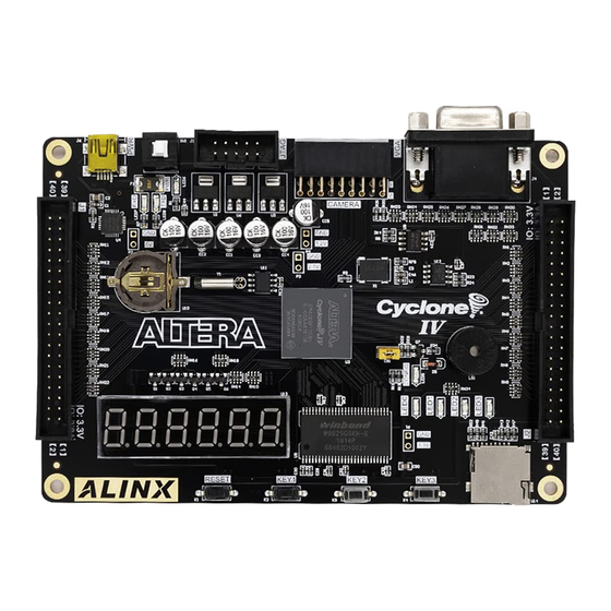
AX301 User Manual This development board is an entry-level product of ALTERA FPGA, mainly for FPGA beginners, model EP4CE6F17C8, is a 256-pin FBGA package. The development of the entire development board is practical, there are two 40-pin 2.54 standard expansion port, a total of 68 IO, in addition to retain the 5V power supply, 3.3V power supply, there are... -
Page 6: Power
- A 6-bit digital tube, 6-digit dynamic display. 2. Power The AX301 development board is powered by USB, and the MINI USB cable is used to connect the development board with the USB of the computer. Pressing the power switch will not only supply power to the development board. -
Page 7: Fpga
AX301 User Manual USB POWER PORT 2.5V AMS1117- FUSE SWITCH 3.3V AMS1117- AMS1117- 1.2V 1.2V Figure 2-1 The development board is powered by USB and generates three power supplies of +3.3V, +2.5V, and +1.2V through the 3 LDO power chip, respectively, to meet the BANK voltage and core voltage of the FPGA. -
Page 8: Jtag
AX301 User Manual 3.1 JTAG First of all ,we talk about FPGA configuration and debugging interface: JTAG interface. The function of the JTAG interface is to download the compiled program (.sof) to the FPGA or download the FLASH configuration program (.jic) to the SPI FLASH. After the sof file is downloaded to the FPGA, it will be lost after power-off ,so we need to download it again after the power-on. -
Page 9: M Crystal
AX301 User Manual Figure 3-3 In addition, there are many pins in the FPGA that need to be connected to GND to ensure a stable reference ground within the FPGA. The GND connected to the FPGA is shown in Figure 3-4. -
Page 10: Spi Flash
AX301 User Manual frequency division and frequency multiplication. Other frequency clocks. Figure 4-1 Clock pin assignment: Signal Name 5. SPI Flash The development board uses a 16Mbit-sized SPI FLASH chip, M25P16, which uses the 3.3V CMOS voltage standard and completely replaces the ALTERA configuration chip EPCS16. -
Page 11: Sdram
AX301 User Manual Configure chip pin assignment: Signal Name DCLK nCSO DATA0 ASDO 6. SDRAM The development board contains a SDRAM chip, model: HY57V2562GTR, capacity: 256Mbit (16M*16bit), 16bit bus. SDRAM can be used for data cache, such as data collected by the camera, temporarily stored in SDRAM, and then displayed through the VGA interface. -
Page 12: Eeprom
AX301 User Manual S_DQM<0> S_DQM<1> S_BA<0> S_BA<1> S_A<0> S_A<1> S_A<2> S_A<3> S_A<4> S_A<5> S_A<6> S_A<7> S_A<8> S_A<9> S_A<10> S_A<11> S_A<12> S_DB<0> S_DB<1> S_DB<2> S_DB<3> S_DB<4> S_DB<5> S_DB<6> S_DB<7> S_DB<8> S_DB<9> S_DB<10> S_DB<11> S_DB<12> S_DB<13> S_DB<14> S_DB<15> 7. EEPROM The board contains a EEPROM, model 24LC04, with a capacity of 4Kbit (2*256*8bit) and consists of two 256-byte blocks that communicate through the IIC bus. -
Page 13: Rtc
AX301 User Manual lost. This kind of chip is simple to operate and has a very high price/performance ratio. Therefore, although the capacity ratio is high, the price is very low, which is a good choice for products that require high costs. Figure 7-1 shows the EEPROM schematic. -
Page 14: Usb To Uart
AX301 User Manual Figure 8-1 DS1302 pin assignment: Signal Name RTC_SClK RTC_nRST RTC_DATA 9. USB TO UART The development board includes the USB-UAR chip of Silicon Labs CP2102GM. The USB interface uses the MINI USB interface. This USB interface implements the power supply function. -
Page 15: Vga Port
AX301 User Manual At the same time, two LED indicators (LED7, LED8) are set for the serial port signal. LED7 and LED8 will indicate whether the serial port has data to send or if there is data accepted, as shown in Figure 9-2. - Page 16 AX301 User Manual Figure 10-2 VGA pin assignment: Explain Signal Name VGA_D[0] BLUE[0] VGA_D[1] BLUE[1] VGA_D[2] BLUE[2] VGA_D[3] BLUE[3] VGA_D[4] BLUE[4] VGA_D[5] GREEN[0] VGA_D[6] GREEN[1] VGA_D[7] GREEN[2] VGA_D[8] GREEN[3] VGA_D[9] GREEN[4] VGA_D[10] GREEN[5] VGA_D[11] RED[0] VGA_D[12] RED[1] VGA_D[13] RED[2] VGA_D[14]...
-
Page 17: Sd Card Slot
AX301 User Manual VGA_D[15] RED[4] VGA_HS Line synchronization signal VGA_VS Field synchronization signal 11. SD Card Slot SD card is a very common storage device nowadays. The SD card that we have expanded supports SPI mode. The SD card used is a MicroSD card. The schematic is shown in Figure 11-1. -
Page 18: Key
AX301 User Manual Figure 12-1 LED pin assignment: Signal Name LED0 LED1 LED2 LED3 13. KEY The board contains 4 independent buttons, 3 user buttons (KEY1~KEY1), and 1 function button (RESET). The buttons are all low pressed as low level (0) and released as high level (1). -
Page 19: Camera Port
AX301 User Manual 14. Camera Port The development board contains an 18-pin CMOS camera interface that can be connected to the camera module to enable video capture. After the capture, the display can be connected via a TFT LCD screen or a VGA port. - Page 20 AX301 User Manual digital tube has one more “point” than the seven-segment digital tube. The digital tube we use is a 6-digit eight-segment digital tube, and the segment structure of the digital tube is shown in Figure 15-1. Figure 15-1 The digital tube we use is a common anode digital tube.
-
Page 21: Buzzer
AX301 User Manual Digital Tube pin assignment: Explain Signal Name DIG[0] DIG[1] DIG[2] DIG[3] DIG[4] DIG[5] DIG[6] DIG[7] Digital Tube 1 SEL[0] Digital Tube 2 SEL[1] Digital Tube 3 SEL[2] Digital Tube 4 SEL[3] Digital Tube 5 SEL[4] Digital Tube 6 SEL[5] 16. -
Page 22: Expansion Port
AX301 User Manual Buzzer pin assignment: Signal Name BUZZER 17. Expansion Port The development board reserves 2 expansion ports, and the expansion port has 40 signals, 1 5V power supply, 2 3.3V power supplies, 3 grounds, and 34 IO ports. These IO ports are independent IO ports and are not multiplexed with other devices. - Page 23 AX301 User Manual D3V3 D3V3 J2 pin assignment: Signal Name Pin Name Pin Number VCC5V D3V3 D3V3 23 / 23 Http://www.alinx.com.cn 23 / 23...
Need help?
Do you have a question about the AX301 and is the answer not in the manual?
Questions and answers