Table of Contents
Advertisement
Quick Links
Advertisement
Table of Contents

Related Manuals for Alinx ZYNQ AC7Z035


Summary of Contents for Alinx ZYNQ AC7Z035
- Page 1 ZYNQ7000 FPGA Development Platform AC7Z035 System on Module...
-
Page 2: Version Record
ZYNQ FPGA Development Board AC7Z035 User Manual Version Record Version Date Release By Description Rev 1.0 2020-06-24 Rachel Zhou First Release Amazon Store: https://www.amazon.com/alinx 2 / 33... -
Page 3: Table Of Contents
Part 7: LED Light ..................20 Part 8: Reset Circuit ................21 Part 9: Power Supply ................22 Part 10: AC7Z035 Core Board Size Dimension ........24 Part 11: Board to Board Connectors pin assignment ......25 Amazon Store: https://www.amazon.com/alinx 3 / 33... -
Page 4: Part 1: Ac7Z035 Core Board Introduction
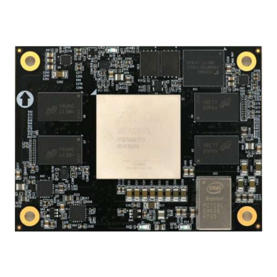
IO, this core board will be a good choice. Moreover, the IO connection part, the routing between the ZYNQ chip and the interface is equal length and differential processing, and the core board size is only 80*60 (mm), which is very suitable for secondary development. Amazon Store: https://www.amazon.com/alinx 4 / 33... - Page 5 ZYNQ FPGA Development Board AC7Z035 User Manual Figure 1-1: AC7Z035 Core Board (Front View) Figure 1-2: AC7Z035 Core Board (Rear View) Amazon Store: https://www.amazon.com/alinx 5 / 33...
-
Page 6: Part 2: Zynq Chip
The main parameters of the PS system part are as follows: ARM dual-core CortexA9-based application processor, ARM-v7 architecture, up to 800MHz 32KB level 1 instruction and data cache per CPU, 512KB level 2 cache 2 CPU shares Amazon Store: https://www.amazon.com/alinx 6 / 33... - Page 7 17 external differential input channels, 1MBPS XC7Z035-2FFG676I chip speed grade is -2, industrial grade, package is FGG676, pin pitch is 1.0mm the specific chip model definition of ZYNQ7000 series is shown in Figure 2-2 Amazon Store: https://www.amazon.com/alinx 7 / 33...
- Page 8 ZYNQ FPGA Development Board AC7Z035 User Manual Figure 2-2: The Specific Chip Model Definition of ZYNQ7000 Series Figure 2-3: The XC7Z035 chip used on the Core Board Amazon Store: https://www.amazon.com/alinx 8 / 33...
-
Page 9: Part 3: Ddr3 Dram
The hardware design of DDR3 requires strict consideration of signal integrity. We have fully considered the matching resistor/terminal resistance, trace impedance control, and trace length control in circuit design and PCB design to ensure high-speed and stable operation of DDR3. Amazon Store: https://www.amazon.com/alinx 9 / 33... - Page 10 Figure 3-2: The Schematic Part of DDR3 DRAM on the PL side PS side DDR3 DRAM pin assignment: Signal Name ZYNQ Pin Name ZYNQ Pin Number PS_DDR_DQS_P0_502 PS_DDR3_DQS0_P PS_DDR_DQS_N0_502 PS_DDR3_DQS0_N PS_DDR_DQS_P1_502 PS_DDR3_DQS1_P PS_DDR_DQS_N1_502 PS_DDR3_DQS1_N PS_DDR_DQS_P2_502 PS_DDR3_DQS2_P PS_DDR_DQS_N2_502 PS_DDR3_DQS2_N Amazon Store: https://www.amazon.com/alinx 10 / 33...
- Page 11 PS_DDR_DQ17_502 PS_DDR3_D17 PS_DDR_DQ18_502 PS_DDR3_D18 PS_DDR_DQ19_502 PS_DDR3_D19 PS_DDR_DQ20_502 PS_DDR3_D20 PS_DDR_DQ21_502 PS_DDR3_D21 PS_DDR_DQ22_502 PS_DDR3_D22 PS_DDR_DQ23_502 PS_DDR3_D23 PS_DDR_DQ24_502 PS_DDR3_D24 PS_DDR_DQ25_502 PS_DDR3_D25 PS_DDR_DQ26_502 PS_DDR3_D26 PS_DDR_DQ27_502 PS_DDR3_D27 PS_DDR_DQ28_502 PS_DDR3_D28 PS_DDR_DQ29_502 PS_DDR3_D29 PS_DDR_DQ30_502 PS_DDR3_D30 PS_DDR_DQ31_502 PS_DDR3_D31 PS_DDR_DM0_502 PS_DDR3_DM0 PS_DDR_DM1_502 PS_DDR3_DM1 Amazon Store: https://www.amazon.com/alinx 11 / 33...
- Page 12 PS_DDR_CAS_B_502 PS_DDR3_CAS PS_DDR_WE_B_502 PS_DDR3_WE PS_DDR_ODT_502 PS_DDR3_ODT PS_DDR_DRST_B_502 PS_DDR3_RESET PS_DDR_CKP_502 PS_DDR3_CLK0_P PS_DDR_CKN_502 PS_DDR3_CLK0_N PS_DDR_CKE_502 PS_DDR3_CKE PL side DDR3 DRAM pin assignment: Signal Name ZYNQ Pin Name ZYNQ Pin Number IO_L3P_T0_DQS_33 PL_DDR3_DQS0_P IO_L3N_T0_DQS_33 PL_DDR3_DQS0_N IO_L9P_T1_DQS_33 PL_DDR3_DQS1_P Amazon Store: https://www.amazon.com/alinx 12 / 33...
- Page 13 IO_L11P_T1_SRCC_33 PL_DDR3_D14 IO_L10P_T1_33 PL_DDR3_D15 IO_L18P_T2_33 PL_DDR3_D16 IO_L14P_T2_SRCC_33 PL_DDR3_D17 IO_L14N_T2_SRCC_33 PL_DDR3_D18 IO_L13P_T2_MRCC_33 PL_DDR3_D19 IO_L16P_T2_33 PL_DDR3_D20 IO_L17P_T2_33 PL_DDR3_D21 IO_L16N_T2_33 PL_DDR3_D22 IO_L17N_T2_33 PL_DDR3_D23 IO_L23P_T3_33 PL_DDR3_D24 IO_L22N_T3_33 PL_DDR3_D25 IO_L19P_T3_33 PL_DDR3_D26 IO_L20N_T3_33 PL_DDR3_D27 IO_L24P_T3_33 PL_DDR3_D28 IO_L20P_T3_33 PL_DDR3_D29 IO_L24N_T3_33 PL_DDR3_D30 Amazon Store: https://www.amazon.com/alinx 13 / 33...
-
Page 14: Part 4: Qspi Flash
PL_DDR3_BA2 IO_L14N_T2_SRCC_34 PL_DDR3_S0 IO_L19P_T3_34 PL_DDR3_RAS IO_L20N_T3_34 PL_DDR3_CAS IO_L20P_T3_34 PL_DDR3_WE IO_L22P_T3_34 PL_DDR3_ODT IO_L16N_T2_34 PL_DDR3_RESET IO_L21P_T3_DQS_34 PL_DDR3_CLK0_P IO_L21N_T3_DQS_34 PL_DDR3_CLK0_N IO_L24P_T3_34 PL_DDR3_CKE Part 4: QSPI Flash The FPGA core board AC7Z035 is equipped with two 256MBit Quad-SPI Amazon Store: https://www.amazon.com/alinx 14 / 33... - Page 15 ZYNQ chip. In the system design, the GPIO port functions of these PS ports need to be configured as the QSPI FLASH interface. Figure 4-1 shows the QSPI Flash in the schematic. Figure 4-1: QSPI Flash in the schematic Configure chip pin assignments: Amazon Store: https://www.amazon.com/alinx 15 / 33...
-
Page 16: Part 5: Emmc Flash
ZYNQ chip. In the system design, the GPIO port functions of these PS ports need to be configured as the SD interface. Figure 5-1 shows the eMMC Flash in the schematic. Amazon Store: https://www.amazon.com/alinx 16 / 33... -
Page 17: Part 6: Clock Configuration
The core system provides a reference clock for the PS system, the PL logic section, and the GTX transceiver, allowing the PS system and PL logic to work independently. The schematic diagram of the clock circuit design is shown in Figure 6-1: Amazon Store: https://www.amazon.com/alinx 17 / 33... - Page 18 PS_CLK_500 of the BANK500 of the ZYNQ chip. The schematic diagram is shown in Figure 2-6-2: Figure 6-2: Active crystal oscillator to the PS section PS Clock Pin Assignment Signal Name ZYNQ Pin PS_CLK Amazon Store: https://www.amazon.com/alinx 18 / 33...
- Page 19 The FPGA core board AC7Z035 provides a 125Mhz reference clock for the GTX transceiver. The reference clock is connected to the reference clock input of the BANK111, REFCLK1P/REFCLK1N. The schematic diagram of the clock source is shown in Figure 6-4. Amazon Store: https://www.amazon.com/alinx 19 / 33...
-
Page 20: Part 7: Led Light
When the IO voltage connected to the user LED is high, the user LED is off. When the connection IO voltage is low, the user LED will be lit. The schematic diagram of the LED light Amazon Store: https://www.amazon.com/alinx 20 / 33... -
Page 21: Part 8: Reset Circuit
ZYNQ system. The schematic diagram of the reset connection is shown in Figure 8-1: PS_POR_B Reset Chip SYS_RESET ZYNQ BANK (TCM811) (Connect to carrier board) Figure 8-1: Reset circuit connection diagram Amazon Store: https://www.amazon.com/alinx 21 / 33... -
Page 22: Part 9: Power Supply
+5V generates +1.0V ZYNQ core power through DCDC power chip EM2130L01QI. EM2130 output current is up to 20A, which is enough to meet the current demand of ZYNQ core voltage. The +5V power supply then uses Amazon Store: https://www.amazon.com/alinx 22 / 33... - Page 23 +1.0V->+1.8V->(+1.5 V, +3.3V, VCCIO12,VCCIO13) circuit design to ensure the normal operation of the chip. The physical diagram of the power circuit on the AX7Z035 core board is shown in Figure 9-2: Amazon Store: https://www.amazon.com/alinx 23 / 33...
-
Page 24: Part 10: Ac7Z035 Core Board Size Dimension
ZYNQ FPGA Development Board AC7Z035 User Manual Figure 9-2: Power Supply on the AX7Z035 Core Board Part 10: AC7Z035 Core Board Size Dimension Figure 10-1: AC7Z035 Core Board Size Dimension Amazon Store: https://www.amazon.com/alinx 24 / 33... -
Page 25: Part 11: Board To Board Connectors Pin Assignment
B13_L10_P AA22 B13_L13_P AD20 B13_L15_N AF20 B13_L14_N AC22 B13_L15_P AF19 B13_L14_P AC21 B13_L23_N B13_L7_P AE22 B13_L23_P B13_L7_N AF22 B13_L22_P AA19 B13_L20_P AA20 B13_L22_N AB19 B13_L20_N AB20 B13_L17_N AD19 B13_L18_N AF18 B13_L17_P AD18 B13_L18_P AE18 Amazon Store: https://www.amazon.com/alinx 25 / 33... - Page 26 AA17 B12_L4_P AB11 B12_L20_P AB17 B12_L4_N AB10 B12_L20_N AB16 B12_L7_P AE10 B12_L8_N AF12 B12_L7_N AD10 B12_L8_P AE12 B12_L24_P B12_L21_P AC17 B12_L24_N B12_L21_N AC16 B12_L3_N AA10 B12_L17_P AE16 B12_L3_P B12_L17_N AE15 B12_L11_P AC12 B12_L22_P AA15 Amazon Store: https://www.amazon.com/alinx 26 / 33...
- Page 27 AA13 B12_L9_P AE11 B12_L6_N AA12 B12_L9_N AF10 B12_L1_P B12_L2_P AB12 B12_L1_N B12_L2_N AC11 Pin assignment of J30 connector ZYNQ Pin ZYNQ Pin J30 Pin Signal Name J30 Pin Signal Name Number Number BANK112_TX0_N BANK112_RX0_N Amazon Store: https://www.amazon.com/alinx 27 / 33...
- Page 28 ZYNQ FPGA Development Board AC7Z035 User Manual BANK112_TX0_P BANK112_RX0_P BANK112_TX1_N BANK112_RX1_N BANK112_TX1_P BANK112_RX1_P BANK112_TX2_N BANK112_RX2_N BANK112_TX2_P BANK112_RX2_P BANK112_TX3_N BANK112_RX3_N BANK112_TX3_P BANK112_RX3_P BANK112_CLK0_N BANK112_CLK1_N BANK112_CLK0_P BANK112_CLK1_P BANK111_RX3_N BANK111_RX3_P BANK111_TX3_N BANK111_TX3_P BANK111_RX2_N BANK111_RX2_P BANK111_TX2_N BANK111_TX2_P BANK111_RX1_N BANK111_RX1_P BANK111_TX1_N BANK111_TX1_P Amazon Store: https://www.amazon.com/alinx 28 / 33...
- Page 29 ZYNQ Pin ZYNQ Pin J31 Pin Signal Name J31 Pin Signal Name Number Number FPGA_TCK FPGA_TDI FPGA_TMS FPGA_TDO B35_L3_P B35_L2_P B35_L3_N B35_L2_N B35_L7_N B35_L6_P B35_L7_P B35_L6_N B35_L4_P B35_L23_P B35_L4_N B35_L23_N B35_L5_N B35_L22_P B35_L5_P B35_L22_N Amazon Store: https://www.amazon.com/alinx 29 / 33...
- Page 30 ZYNQ FPGA Development Board AC7Z035 User Manual B35_L8_P B35_L24_N B35_L8_N B35_L24_P B35_L12_P B35_L11_N B35_L12_N B35_L11_P B35_L9_P B35_L19_N B35_L9_N B35_L19_P B35_L1_N B35_L21_N B35_L1_P B35_L21_P B35_L17_N B35_L14_P B35_L17_P B35_L14_N B35_L20_N B35_L18_P B35_L20_P B35_L18_N B35_L10_N B35_L15_N B35_L10_P B35_L15_P B35_L13_N B35_L13_P B35_L16_N B35_L16_P Amazon Store: https://www.amazon.com/alinx 30 / 33...
- Page 31 Pin assignment of J32 connector ZYNQ Pin ZYNQ Pin J32 Pin Signal Name J32 Pin Signal Name Number Number PS_MIO5 PS_MIO17 PS_MIO4 PS_MIO18 PS_MIO14 PS_MIO19 PS_MIO15 PS_MIO20 PS_MIO52 PS_MIO16 PS_MIO53 PS_MIO21 PS_MIO7 PS_MIO26 PS_MIO25 PS_MIO40 PS_MIO24 Amazon Store: https://www.amazon.com/alinx 31 / 33...
- Page 32 ZYNQ FPGA Development Board AC7Z035 User Manual PS_MIO41 PS_MIO23 PS_MIO42 PS_MIO27 PS_MIO43 PS_MIO22 PS_MIO44 PS_MIO30 PS_MIO45 PS_MIO29 PS_MIO36 PS_MIO31 PS_MIO32 PS_MIO33 PS_MIO34 PS_MIO35 PS_MIO28 PS_MIO37 PS_MIO38 PS_MIO39 B13_L1_P AA25 B13_L11_P AD23 B13_L1_N AB25 B13_L11_N AD24 Amazon Store: https://www.amazon.com/alinx 32 / 33...
- Page 33 ZYNQ FPGA Development Board AC7Z035 User Manual B13_L6_P AA24 B13_L4_P AD25 B13_L6_N AB24 B13_L4_N AD26 B13_L2_N AC26 B13_L5_P AF24 B13_L2_P AB26 B13_L5_N AF25 B13_L12_P AC23 B13_L3_P AE25 B13_L12_N AC24 B13_L3_N AE26 Amazon Store: https://www.amazon.com/alinx 33 / 33...
Need help?
Do you have a question about the ZYNQ AC7Z035 and is the answer not in the manual?
Questions and answers