
Subscribe to Our Youtube Channel
Related Manuals for Intel Cyclone 10 GX FPGA


Summary of Contents for Intel Cyclone 10 GX FPGA
- Page 1 ® ® Intel Cyclone 10 GX FPGA Development Kit User Guide Subscribe UG-20105 | 2017.12.18 Send Feedback Latest document on the web: HTML...
- Page 2 2 Getting Started........................ 7 2.1 Installing the Quartus Prime Software............... 7 2.2 Development Kit Package..................8 2.3 Installing the Intel FPGA Download Cable Driver............8 3 Development Kit Setup....................10 3.1 Setting up the Development Kit................10 3.2 Default Switch and Jumper Settings................ 10 4 Development Board Components...................
- Page 3 A Additional Information....................60 A.1 Safety and Regulatory Information................60 A.1.1 Safety Warnings..................61 A.1.2 Safety Cautions..................62 A.2 Compliance and Conformity Statements..............64 B Revision History......................65 B.1 User Guide Revision History................... 65 ® ® Intel Cyclone 10 GX FPGA Development Kit User Guide...
-
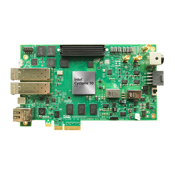
Page 4: Overview
Intel's standard warranty, but reserves the right to make changes to any products and services Registered at any time without notice. Intel assumes no responsibility or liability arising out of the application or use of any information, product, or service described herein except as expressly agreed to in writing by Intel. Intel customers are advised to obtain the latest version of device specifications before relying on any published information and before placing orders for products or services. - Page 5 1 FPGA reset Pushbutton to reset the FPGA logic Switches • 4 User DIP Switches • DIP switch for MSEL • DIP switch for JTAG chain selection • DIP switch for clock source selection ® ® Intel Cyclone 10 GX FPGA Development Kit User Guide...
-
Page 6: Recommended Operating Conditions
Without proper anti-static handling, the board could be damaged. Use anti-static handling precautions when handling the board. Note: This development kit should not be operated in a Vibration environment. ® ® Intel Cyclone 10 GX FPGA Development Kit User Guide... -
Page 7: Getting Started
Intel's standard warranty, but reserves the right to make changes to any products and services Registered at any time without notice. Intel assumes no responsibility or liability arising out of the application or use of any information, product, or service described herein except as expressly agreed to in writing by Intel. Intel customers are advised to obtain the latest version of device specifications before relying on any published information and before placing orders for products or services. -
Page 8: Development Kit Package
1. Download the development kit package from the Intel Cyclone 10 GX FPGA Development Kit link on the Intel website. 2. Unzip the Intel Cyclone 10 GX FPGA Development Kit package contents to your machine's local hard drive. 3. The package creates the directory structure shown in the figure below. - Page 9 2 Getting Started UG-20105 | 2017.12.18 On the Intel website, navigate to the Cable and Adapter Drivers Information link to locate the table entry for your configuration and click the link to access the instructions. ® ® Intel Cyclone 10 GX FPGA Development Kit User Guide...
-
Page 10: Development Kit Setup
Intel's standard warranty, but reserves the right to make changes to any products and services Registered at any time without notice. Intel assumes no responsibility or liability arising out of the application or use of any information, product, or service described herein except as expressly agreed to in writing by Intel. Intel customers are advised to obtain the latest version of device specifications before relying on any published information and before placing orders for products or services. - Page 11 3 Development Kit Setup UG-20105 | 2017.12.18 Board Label Switch Default Position Function S5.2 OPEN/OFF/1 Enable Intel Cyclone 10 GX FPGA JTAG S6.1 OPEN/OFF/1 Reserved, no function defined S6.2 OPEN/OFF/1 Reserved, no function defined S9.1 OPEN/OFF/1 User available Digital Input 0 S9.2...
-
Page 12: Development Board Components
Intel's standard warranty, but reserves the right to make changes to any products and services Registered at any time without notice. Intel assumes no responsibility or liability arising out of the application or use of any information, product, or service described herein except as expressly agreed to in writing by Intel. Intel customers are advised to obtain the latest version of device specifications before relying on any published information and before placing orders for products or services. - Page 13 Type-B Micro USB Connector for programming and debugging the FPGA 10-pin header Optional JTAG direct via 10-pin header for external download cables DIP-SW: Intel Cyclone 10 GX FPGA Configuration Mode ON/Closed/0 OFF/Open/1 Press this button to cycle through different PFL loads FPGA Push Button...
- Page 14 4-bit user DIP switches, low when set to ON Clocks 50 MHz Oscillator 50 MHz crystal oscillator for logic of two Intel MAX 10 FPGA devices, 3.3V LVCMOS 50 MHz Oscillator 50 MHz crystal oscillator for general purpose logic of Intel Cyclone 10 GX FPGA, 1.8V LVCMOS...
-
Page 15: Cyclone 10 Gx Fpga
UG-20105 | 2017.12.18 4.2 Cyclone 10 GX FPGA The target FPGA device this kit is designed to work with is the Intel Cyclone 10 GX 10CX220YF780E5G FPGA. It is the device with the fastest speed, largest resource and biggest package in the Intel Cyclone 10 GX FPGA series. - Page 16 1.8V CMOS input From U2 (Intel MAX C10_TMS 1.8 V CMOS input From U2 (Intel MAX C10_TDI 1.8 V CMOS input To U2 (Intel MAX 10) C10_TDO Configuration 1.8 V CMOS input 100 MHz, for C10_CLKUSR calibration 1.8 V CMOS input...
- Page 17 Description From U3 (Intel MAX for FPPx16 1.8 V CMOS input From U3 (Intel MAX FPP [0:15] 1.8 V CMOS output To U2 (Intel MAX 10) CVP_CONFDONE UBII Side Bus 1.8 V CMOS input From U2 (Intel MAX M10_USB_DATA [0:7] 1.8 V CMOS input...
- Page 18 To golden finger, PCIE_WAKEn reserved 1.8 V CMOS output To golden finger PCIE_SMBCLK 1.8 V CMOS inout To golden finger PCIE_SMBDAT 1.8 V CMOS input To golden finger PCIE_PERSTn continued... ® ® Intel Cyclone 10 GX FPGA Development Kit User Guide...
-
Page 19: Max 10 System Controller
Instant on support • Integrated analog-to-digital converter (ADC) • Single-chip Nios II soft core processor support Intel MAX 10 devices are the ideal solution for system management, I/O expansion, communication control planes, industrial, automotive, and consumer applications. ® ® Intel... - Page 20 4 Development Board Components UG-20105 | 2017.12.18 Table 6. Summary of Features for Intel MAX 10 Devices Feature Description Technology 55 nm TSMC Embedded Flash (Flash + SRAM) process technology Packaging • Low cost, small form factor packages—support multiple packaging technologies and pin pitches •...
-
Page 21: Fpga Configuration
4.4 FPGA Configuration JTAG The JTAG topology of the board is shown in the figure below. An on-board USB Blaster is implemented with the Intel MAX 10. It is in the form of a micro-USB type-B connector (J9). Figure 3. - Page 22 AS X4 EPCQ-L The Intel Cyclone 10 GX FPGA device is configured with two modes: ASx4 or FPP x16. The AS x4 mode uses an EPCQ-L 1024 to store the image. A dedicated Intel MAX 10 device is used to implement PFL. It interfaces with two pieces of x16 parallel NOR flash devices to get a x32 bus width.
-
Page 23: Status And User I/O Elements
MT28EW01GABA1LPC-0SITES provided with the board. For the Intel Cyclone 10 GX FPGA device, the image size is less than 85 Mb. Multiple images can be stored and selected by the user. The image to be used can be selected with a group of Push Buttons and LEDs. -
Page 24: Pushbuttons
User available Digital Input USER_DIP2 S15.2 User available Digital Input USER_DIP3 S6.1 Reserved, No Function CFG_M10_PGM0 S6.2 CFG_M10_PGM0 S1.1 Intel Cyclone 10 GX MSEL C10_MSEL0 S1.2 C10_MSEL1 S3.1 Input selection for clock Si5340_INSEL0 generator chip, the Si5332 S3.2 on this board Si5340_INSEL1... -
Page 25: Leds
Trigger reconfiguration to Intel Cyclone 10 GX FPGA. The image SYS_CONFIG_PB used for configuration is selected with PGM_SEL button and indicated by PGM_NUM LEDs Trigger logic reset to Intel Cyclone 10 GX FPGA logic. The state C10_RESETn_PB of the configured logic is reset, the configuration remains unchanged. -
Page 26: Clocks
. Si53307 is a clock buffer. With Si570 + Si53307, a high frequency 7'b110_0110 reference clock at frequency up to 725 MHz is available for Intel Cyclone 10 GX FPGA Transceiver. Other clocks are generated with an programmable clock generator Si5332... -
Page 27: Memory
4.7 Memory 4.7.1 EMIF with DDR3 The Intel Cyclone 10 GX FPGA device supports DDR3 memory up to 933 MHz. On this development kit, a DDR3 x40 at 933 MHz is implemented with DDR3 devices. The EMIF uses continuous banks in the same column. To achieve 933 MHz speed, EMIF uses bank 2J and 2K to support 40-bit width at 933 MHz. - Page 28 Intel Cyclone 10 GX EN6337QI VCCH/ VCCA_PLL/ VCCPT/ VCCBAT VCCPT/ VCCA_PLL/ VCCH_GXB/ VCCBAT VCCPGM/ VCCIO EN_GROUP4 IO_1.8V, 1 A VCCPGM/ VCCIO/ System Intel MAX 10/ EN6337QI Configuration Intel MAX 10/ Si5332/ USB EN_GROUP4 C10_1.5V, 1.8 A EN6337QI FPGA Quick Power DOWN Sequencing:...
-
Page 29: Transceivers Interfaces And Communication Ports
4.9 Transceivers Interfaces and Communication Ports 4.9.1 Transceiver Channels The Intel Cyclone 10 GX FPGA device has 12 channels of transceivers that work at 12.5 Gbps. The transceivers are organized in two banks, each bank has six channels. Table 15. -
Page 30: Usb3.1 Type-C Interface
4.9.4 USB3.1 Type-C Interface A USB3.1 Type-C interface (J8) is provided on the PCIe bracket. The interface supports SuperSpeed up to 10 Gbps as well as the backward compatible support of USB2.0. ® ® Intel Cyclone 10 GX FPGA Development Kit User Guide... - Page 31 VBUS only when the port is in DFP mode. The power application can be controlled by the FPGA too. The signal is active high because of the NMOS USB_PWEN inverter. ® ® Intel Cyclone 10 GX FPGA Development Kit User Guide...
-
Page 32: Fpga Mezzanine Card (Fmc) Interface
12G SDI: Semtech RDK-12GSRD-ALTRA00 Evaluation Board • 8G DisplayPort: Bitec FMC DisplaPort Daughter Card • 6G HDMI 2.0: Bitec FMC HDMI Daughter Card Table 17. FMC Signals Intel Cyclone 10 GX FPGA Development Kit DisplayPort HDMI Signal V57.1 Name Signal Name Pin Number... - Page 33 4 Development Board Components UG-20105 | 2017.12.18 Intel Cyclone 10 GX FPGA Development Kit DisplayPort HDMI Signal V57.1 Name Signal Name Pin Number SDI FMC DisplayPort HDMI FMC Signal Name FMC Signal Signal Name Name DP7_C2M_N DP7_C2M_N DP8_C2M_P DP8_C2M_P DP8_C2M_N...
- Page 34 4 Development Board Components UG-20105 | 2017.12.18 Intel Cyclone 10 GX FPGA Development Kit DisplayPort HDMI Signal V57.1 Name Signal Name Pin Number SDI FMC DisplayPort HDMI FMC Signal Name FMC Signal Signal Name Name GBTCLK1_M2C GTBCLK1_M2C GBTCLK1_M2C GTBCLK1_M2C LA Bank...
- Page 35 4 Development Board Components UG-20105 | 2017.12.18 Intel Cyclone 10 GX FPGA Development Kit DisplayPort HDMI Signal V57.1 Name Signal Name Pin Number SDI FMC DisplayPort HDMI FMC Signal Name FMC Signal Signal Name Name FMC_LA_TXN5 LA11_N LA_TX_N5 FMC_GS12181 _GPIO3...
- Page 36 4 Development Board Components UG-20105 | 2017.12.18 Intel Cyclone 10 GX FPGA Development Kit DisplayPort HDMI Signal V57.1 Name Signal Name Pin Number SDI FMC DisplayPort HDMI FMC Signal Name FMC Signal Signal Name Name FMC_LA_TXN1 LA24_N LA_TX_N12 FMC_FPGA_FL TX_CAD_INV_F...
-
Page 37: Base-T Ethernet Connector
4 Development Board Components UG-20105 | 2017.12.18 Intel Cyclone 10 GX FPGA Development Kit DisplayPort HDMI Signal V57.1 Name Signal Name Pin Number SDI FMC DisplayPort HDMI FMC Signal Name FMC Signal Signal Name Name FMCA_CLK_M2 CLK1_M2C_P CLK_M2C_P1 C_P1 FMCA_CLK_M2... - Page 38 MDC/MDIO is connected to the FPGA device through a level translator. 4.9.7 I C/PMBUS The power and various peripherals are managed by I C/PMBUS. The topology of the C bus is shown in the figure below. ® ® Intel Cyclone 10 GX FPGA Development Kit User Guide...
- Page 39 EM2130 EM2130 LTC2497 TMP512A 3.3 V 0.9 V I-Sense I/V/T-Sense (110_0000) (110_0110) (001_0100) (101_1100) PMBUS 3.3 V System Intel MAX 10 Dongle Configuration (101_0000) HDR4 X1 Intel MAX 10 I2C 3.3 V Si5340 Si5332 Si570 (111_0100) (110_1010) (110_0110) Level I2C 1.8 V Shifter I2C 2.5 V...
-
Page 40: Board Test System
Intel's standard warranty, but reserves the right to make changes to any products and services Registered at any time without notice. Intel assumes no responsibility or liability arising out of the application or use of any information, product, or service described herein except as expressly agreed to in writing by Intel. Intel customers are advised to obtain the latest version of device specifications before relying on any published information and before placing orders for products or services. -
Page 41: Preparing The Board
BTS and Power Monitor share the JTAG bus with other applications like the Nios II debugger and the Signal Tap II Embedded Logic Analyzer. Because the BTS is designed based on the Intel Quartus Prime software, be sure to close other applications before you use the BTS. -
Page 42: Running The Board Test System
Use the Configure Menu to select the design you want to use. Each design example tests different board features. Select a design from this menu and the corresponding tabs become active for testing. ® ® Intel Cyclone 10 GX FPGA Development Kit User Guide... -
Page 43: The System Info Tab
5.3.2 The System Info Tab The System Info tab shows the board's current configuration. The tab displays the contents of the Intel MAX 10 registers, the JTAG chain, the board's MAC address, and other details stored on the board. ®... - Page 44 <package dir>\examples\max10 Newer revisions of this code may be available on the Intel Cyclone 10 GX FPGA Development kit link on the Intel website. The Intel MAX 10 register control allows you to view and change the current Intel MAX 10 register values as described in the table below.
-
Page 45: The Gpio Tab
Configure Resets the system and reloads the FPGA with a design from the CFI flash memory based on the other Intel MAX 10 register values. It works only in FPP mode. Sets the Intel MAX 10 PSO register. Sets the Intel MAX 10 PSR register. Allows PSR to determine the page of flash memory to use for FPGA reconfiguration. -
Page 46: The Epcq Tab
0 contents by default after you configure the FPGA. Note: The EPCQ Tab works only when the board MSEL is configured on AS mode. Figure 14. The Flash Tab ® ® Intel Cyclone 10 GX FPGA Development Kit User Guide... -
Page 47: The Xcvr Tab
Flash Memory Map Displays the flash memory map for the development board. 5.3.5 The XCVR Tab This tab allows you to perform loopback tests on the PCIe and SFP+ ports. ® ® Intel Cyclone 10 GX FPGA Development Kit User Guide... - Page 48 Details: Shows the PLL lock, pattern sync status and number of errors for a single channel. Port Allows you to specify which interface to test. The following port tests are available: ® ® Intel Cyclone 10 GX FPGA Development Kit User Guide...
- Page 49 DC gain: Specifies the DC gain setting for the receiver equalizer in four stage mode. • VGA: Specifies the VGA gain value. Data Type Specifies the type of data contained in the transactions. The following data types are available for analysis: ® ® Intel Cyclone 10 GX FPGA Development Kit User Guide...
-
Page 50: The Fmc Tab
TX and RX performance bars: Show the percentage of maximum theoretical data rate that the requested transactions are able to achieve. 5.3.6 The FMC Tab This tab allows you to perform loopback tests on the FMC port. ® ® Intel Cyclone 10 GX FPGA Development Kit User Guide... - Page 51 Pattern Sync: Shows the pattern synced or not synced state. The pattern is considered synced when the start of he data data sequence is detected. • Details: Shows the PLL lock, pattern sync status and number of errors per channel. ® ® Intel Cyclone 10 GX FPGA Development Kit User Guide...
- Page 52 VGA: Specifies the VGA gain value. Figure 17. PMA Settings Data Type Specifies the type of data contained in the transactions. The following data types are available for analysis. ® ® Intel Cyclone 10 GX FPGA Development Kit User Guide...
-
Page 53: The Ddr3 Tab
TX and RX performance bars - Shows the percentage of maximum theoretical data rate that the requested transactions are able to achieve. 5.3.7 The DDR3 Tab This tab allows you to read and write DDR3 memory on your board. ® ® Intel Cyclone 10 GX FPGA Development Kit User Guide... - Page 54 Write (MBps), Read(MBps) and Total(MBps): Show the number of bytes of data analayzed per second. Error Control This control displays data errors detected during analysis and allows you to insert errors: ® ® Intel Cyclone 10 GX FPGA Development Kit User Guide...
-
Page 55: Power Monitor
The Power Monitor measures and reports current power information and communicates with the Intel MAX 10 device on the board through the JTAG bus. A power monitor circuit attached to the Intel MAX 10 device allows you to measure the power that the FPGA is consuming. - Page 56 Date Record: Record real time voltage, current and power values, and save to a log file. Reset Clears the graph, resets the minimum and maximum values and restarts the Power Monitor. Temperature Displays the temperature of the FPGA and the development kit. ® ® Intel Cyclone 10 GX FPGA Development Kit User Guide...
-
Page 57: Clock Controller
The Clock Controller application sets the Si570 programmable oscillators to any frequency between 10 MHz and 725 MHz. The Clock Control communicates with the Intel MAX 10 on the board through the JTAG bus. The programmable oscillator are connected to the Intel MAX 10 device through a 2-wire serial bus. - Page 58 Sets the programmable oscillator frequency for the selected clock to the value in the Target Frequency control for the programmable oscillators. Frequency changes might take several milliseconds to take effect. You might see glitches on the clock during this period. Intel recommends resetting the FPGA logic after changing frequencies. Figure 21.
- Page 59 OUT4 OUT6 OUT7 take several milliseconds to take effect. You might see glitches on the clock during this period. Intel recommends resetting the FPGA logic after changing frequencies. Import Import register map file generated from Silicon Laboratories ClockBuilder Desktop. ®...
-
Page 60: A Additional Information
Intel's standard warranty, but reserves the right to make changes to any products and services Registered at any time without notice. Intel assumes no responsibility or liability arising out of the application or use of any information, product, or service described herein except as expressly agreed to in writing by Intel. Intel customers are advised to obtain the latest version of device specifications before relying on any published information and before placing orders for products or services. -
Page 61: A.1.1 Safety Warnings
To avoid shock, you must ensure that the power cord is connected to a properly wired and grounded receptacle. Ensure that any equipment to which this product will be attached is also connected to properly wired and grounded receptacles. ® ® Intel Cyclone 10 GX FPGA Development Kit User Guide... -
Page 62: A.1.2 Safety Cautions
Certain components such as heat sinks, power regulators, and processors may be hot. Heatsink fans are not guarded. Power supply fan may be accessible through guard. Care should be taken to avoid contact with these components. ® ® Intel Cyclone 10 GX FPGA Development Kit User Guide... - Page 63 Public Switched Telecommunication Network (PSTN) as it might result in disruption of the network. No formal telecommunication certification to FCC, R&TTE Directive, or other national requirements have been obatined. ® ® Intel Cyclone 10 GX FPGA Development Kit User Guide...
-
Page 64: A.2 Compliance And Conformity Statements
Failure to use wrist straps can damage components within the system. Attention: Please return this product to Intel for proper disposition. If it is not returned, refer to local environmental regulations for proper recycling. Do not dispose of this product in unsorted municipal waste. -
Page 65: B Revision History
Intel's standard warranty, but reserves the right to make changes to any products and services Registered at any time without notice. Intel assumes no responsibility or liability arising out of the application or use of any information, product, or service described herein except as expressly agreed to in writing by Intel. Intel customers are advised to obtain the latest version of device specifications before relying on any published information and before placing orders for products or services.
Need help?
Do you have a question about the Cyclone 10 GX FPGA and is the answer not in the manual?
Questions and answers