
Related Manuals for Intel Arria 10


Summary of Contents for Intel Arria 10
- Page 1 ® ® Intel Arria 10 SoC Development Kit User Guide Online Version 683227 Send Feedback 2023.07.12 UG-20004 Arrow.com. Downloaded from...
-
Page 2: Table Of Contents
4.4.11. The Power Monitor................. 44 4.4.12. The Clock Control...................46 5. Board Components......................48 5.1. Board Overview....................48 5.2. Featured Device: Arria 10 SoC ................51 5.3. MAX V CPLD 5M2210 System Controller..............52 5.4. Configuration...................... 60 5.4.1. System Controller Configuration..............60 5.4.2. FPGA and I/O MUX CPLD Programming over On-Board USB-Blaster II..... 61 5.4.3. - Page 3 5.11. Board Power Supply..................117 5.11.1. Power Distribution System..............118 5.11.2. Power Measurement................118 A. Additional Information....................119 A.1. Document Revision History for the Intel Arria 10 SoC Development Kit User Guide..119 A.2. Compliance and Conformity Statements..............121 A.2.1. CE EMI Conformity Caution..............121 ®...
-
Page 4: Intel ® Arria ® 10 Soc Development Kit Overview
Intel's standard warranty, but reserves the right to make changes to any 9001:2015 products and services at any time without notice. Intel assumes no responsibility or liability arising out of the Registered application or use of any information, product, or service described herein except as expressly agreed to in writing by Intel. - Page 5 Linear Power Jumper J30 FPGA Dongle J32 FMCB Power Header Voltage For more information about the Arria 10 SoC device family, refer to the Arria 10 SoC documentation support page. Related Information Arria 10 Documentation ® ® Intel Arria 10 SoC Development Kit User Guide Send Feedback Arrow.com.
-
Page 6: Board Component Blocks
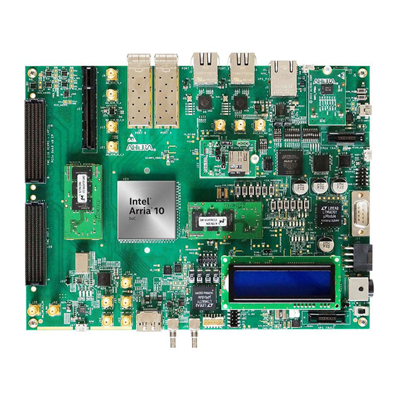
683227 | 2023.07.12 1.2. Board Component Blocks The development board features the following major component blocks: • Arria 10 Soc (10AS066N3F40E2SG) in a 1517-pin FBGA (FineLine Ball-Grid Array) package • FPGA configuration circuitry — Active Serial (AS) x1 or x4 configuration (EPCQ1024L) ®... - Page 7 ® ® 1. Intel Arria 10 SoC Development Kit Overview 683227 | 2023.07.12 • Communication ports — HPS Communication ports: • USB 2.0 port (PHY PN: USB3320C-EZK) • RGMII 10/100/1000 Ethernet port (PHY PN: KSZ9031RNXCA) • USB-UART port (FT232R) •...
-
Page 8: Recommended Operating Conditions
® ® 1. Intel Arria 10 SoC Development Kit Overview 683227 | 2023.07.12 • General user I/O — LEDs and displays • 4x FPGA user LEDs • 4x HPS user LEDs • Configuration load LED • Configuration done LED •... -
Page 9: Handling The Board
® ® 1. Intel Arria 10 SoC Development Kit Overview 683227 | 2023.07.12 1.4. Handling the Board When handling the board, it is important to observe static discharge precautions. Caution: Without proper anti-static handling, the board can be damaged. Therefore, use anti- static handling precautions when touching the board. -
Page 10: Getting Started
Intel's standard warranty, but reserves the right to make changes to any 9001:2015 products and services at any time without notice. Intel assumes no responsibility or liability arising out of the Registered application or use of any information, product, or service described herein except as expressly agreed to in writing by Intel. -
Page 11: Installing The Subscription Edition Of The Quartus Prime Design Software
Quartus Prime Pro Edition Software from the Quartus Prime Pro Edition page in the Download Center of the Altera website. Related Information Quartus Prime Software page ® ® Intel Arria 10 SoC Development Kit User Guide Send Feedback Arrow.com. Downloaded from... -
Page 12: Activating Your License
For the steps to install the SoC EDS Tool Suite, refer to the Altera SoC Embedded Design Suite User Guide. Related Information • ARM Development Studio 5 (DS-5) Altera Edition Toolkit • Altera SoC Embedded Design Suite User Guide ® ® Intel Arria 10 SoC Development Kit User Guide Send Feedback Arrow.com. Downloaded from... -
Page 13: Development Kit Installer
Quartus Prime design software, nor does it include the SoC EDS software development tools. 1. Download the Arria 10 FPGA Development Kit installer from the Arria 10 FPGA Development Kit page of the Altera website. Alternatively, you can request a development kit DVD from the Altera Kit Installations DVD Request Form page of the Altera website. -
Page 14: Sd Card Image With Example Software
24/n MHz (between 10 KHz and 6 MHz, where n represents an integer value.) Related Information Altera Programming Cable Driver Information 2.6. SD Card Image with Example Software The Arria 10 GSRD (Golden System Reference Design) page on Rocketboards.org has instructions to create an SD card image. Related Information GSRD User Manual ®... -
Page 15: Development Board Setup
Intel's standard warranty, but reserves the right to make changes to any 9001:2015 products and services at any time without notice. Intel assumes no responsibility or liability arising out of the Registered application or use of any information, product, or service described herein except as expressly agreed to in writing by Intel. -
Page 16: Default Switch And Jumper Settings
ON (0) = Load user design from flash at power up • OFF (1) = Load factory design from flash at power up security_mode Resvered ® ® Intel Arria 10 SoC Development Kit User Guide Send Feedback Arrow.com. Downloaded from... - Page 17 Switch 4.4 has the following options: • ON (Up) = MSEL2 is 1 • OFF (Down) = MSEL2 is 0 Table 5. MSEL Settings for each Configuration Scheme of Arria 10 SoC Devices Configuration Power-On Reset (POR delay) Valid MSEL [2:0] ccpgm JTAG-based configuration...
- Page 18 SHORT upper 2 pins The directions of these pins are in reference to the board arrangement as in the "Default Switch and Jumper Settings" figure. ® ® Intel Arria 10 SoC Development Kit User Guide Send Feedback Arrow.com. Downloaded from...
- Page 19 3. Development Board Setup 683227 | 2023.07.12 Related Information Board Settings DIP Switch on page 64 ® ® Intel Arria 10 SoC Development Kit User Guide Send Feedback Arrow.com. Downloaded from...
-
Page 20: Board Test System
Intel's standard warranty, but reserves the right to make changes to any 9001:2015 products and services at any time without notice. Intel assumes no responsibility or liability arising out of the Registered application or use of any information, product, or service described herein except as expressly agreed to in writing by Intel. -
Page 21: Preparing The Board
3. Turn on the power to the board, and run the Board Test System. Note: To ensure operating stability, keep the USB cable connected and the board powered on when running the demonstration application. ® ® Intel Arria 10 SoC Development Kit User Guide Send Feedback Arrow.com. -
Page 22: Running The Board Test System
The Board Test System (BTS) will prompt you with a Version Selector window once opened. You can also open the Version Selector window through the Configure tab by clicking Select Silicon Version. Select the silicon version of the Arria 10 device that is installed on your board. - Page 23 3-4 digits of the serial number which can be found on the bottom of your board. Figure 8. Board Serial Number Sticker Table 11. Serial Number Arria 10 SoC Silicon Revision 10ASXSoC00[<0500] 10ASXSoC00[0500-1999] 10ASXSoC00[>1999] ® ®...
-
Page 24: Using The Board Test System
1. On the Configure menu, click the configure command that corresponds to the functionality you wish to test. 2. In the dialog box that appears, click Configure to download the corresponding design to the FPGA. ® ® Intel Arria 10 SoC Development Kit User Guide Send Feedback Arrow.com. Downloaded from... - Page 25 4. Board Test System 683227 | 2023.07.12 Figure 10. Programmer Dialog Window ® ® Intel Arria 10 SoC Development Kit User Guide Send Feedback Arrow.com. Downloaded from...
-
Page 26: The System Info Tab
Indicates the MAC address of the ETH port of the HPS JTAG Chain Shows all the devices currently in the JTAG chain. EEPROM Map Shows the EEPROM map on your board. ® ® Intel Arria 10 SoC Development Kit User Guide Send Feedback Arrow.com. Downloaded from... -
Page 27: The Gpio Tab
Read-only control displays the current state of the board user push buttons. Press a push button on the board to see the graphical display change accordingly. ® ® Intel Arria 10 SoC Development Kit User Guide Send Feedback Arrow.com. Downloaded from... -
Page 28: The Xcvr Tab
Port Allows you to specify which interface to test. The following port tests are available: SFP A x1 SFP B x1 SMA x1 continued... ® ® Intel Arria 10 SoC Development Kit User Guide Send Feedback Arrow.com. Downloaded from... - Page 29 Note: Always click Clear before Start. Stop—Terminates transaction performance analysis. TX and RX performance bars—Show the percentage of maximum theoretical data rate that the requested transactions are able to achieve. ® ® Intel Arria 10 SoC Development Kit User Guide Send Feedback Arrow.com. Downloaded from...
-
Page 30: The Pcie Tab
PLL lock—Shows the PLL locked or unlocked state. Pattern sync—Shows the pattern synced or not synced state. The pattern is considered synced when the start of the data sequence is detected. continued... ® ® Intel Arria 10 SoC Development Kit User Guide Send Feedback Arrow.com. Downloaded from... - Page 31 Equalizer—Specifies the AC gain setting for the receiver equalizer in four stage mode. DC gain—Specifies the DC gain setting for the receiver equalizer in four stage mode. VGA—Specifies the VGA gain value. continued... ® ® Intel Arria 10 SoC Development Kit User Guide Send Feedback Arrow.com. Downloaded from...
- Page 32 Note: Always click Clear before Start. Stop—Terminates transaction performance analysis. TX and RX performance bars—Show the percentage of maximum theoretical data rate that the requested transactions are able to achieve. ® ® Intel Arria 10 SoC Development Kit User Guide Send Feedback Arrow.com. Downloaded from...
-
Page 33: The Fmca Tab
PLL lock—Shows the PLL locked or unlocked state. Pattern sync—Shows the pattern synced or not synced state. The pattern is considered synced when the start of the data sequence is detected. continued... ® ® Intel Arria 10 SoC Development Kit User Guide Send Feedback Arrow.com. Downloaded from... - Page 34 Equalizer—Specifies the AC gain setting for the receiver equalizer in four stage mode. DC gain—Specifies the DC gain setting for the receiver equalizer in four stage mode. VGA—Specifies the VGA gain value. continued... ® ® Intel Arria 10 SoC Development Kit User Guide Send Feedback Arrow.com. Downloaded from...
- Page 35 Note: Always click Clear before Start. Stop—Terminates transaction performance analysis. TX and RX performance bars—Show the percentage of maximum theoretical data rate that the requested transactions are able to achieve. ® ® Intel Arria 10 SoC Development Kit User Guide Send Feedback Arrow.com. Downloaded from...
-
Page 36: The Fmcb Tab
PLL lock—Shows the PLL locked or unlocked state. Pattern sync—Shows the pattern synced or not synced state. The pattern is considered synced when the start of the data sequence is detected. continued... ® ® Intel Arria 10 SoC Development Kit User Guide Send Feedback Arrow.com. Downloaded from... - Page 37 Equalizer—Specifies the AC gain setting for the receiver equalizer in four stage mode. DC gain—Specifies the DC gain setting for the receiver equalizer in four stage mode. VGA—Specifies the VGA gain value. continued... ® ® Intel Arria 10 SoC Development Kit User Guide Send Feedback Arrow.com. Downloaded from...
- Page 38 HF—Selects highest frequency divide-by-2 data pattern 10101010. • LF—Selects lowest frequency divide-by-33 data pattern. Error Control Displays data errors detected during analysis and allows you to insert errors: continued... ® ® Intel Arria 10 SoC Development Kit User Guide Send Feedback Arrow.com. Downloaded from...
- Page 39 Note: Always click Clear before Start. Stop—Terminates transaction performance analysis. TX and RX performance bars—Show the percentage of maximum theoretical data rate that the requested transactions are able to achieve. ® ® Intel Arria 10 SoC Development Kit User Guide Send Feedback Arrow.com. Downloaded from...
-
Page 40: The Ddr3 Tab
136512 Mbps or 17064 MBps. Error Control This control displays data errors detected during analysis and allows you to insert errors: continued... ® ® Intel Arria 10 SoC Development Kit User Guide Send Feedback Arrow.com. Downloaded from... - Page 41 Clear—Resets the Detected errors and Inserted errors counters to zeroes. Number of Addresses to Write and Read Determines the number of addresses to use in each iteration of reads and writes. ® ® Intel Arria 10 SoC Development Kit User Guide Send Feedback Arrow.com. Downloaded from...
-
Page 42: The Ddr4 Tab
136512 Mbps or 17064 MBps. Error Control This control displays data errors detected during analysis and allows you to insert errors: continued... ® ® Intel Arria 10 SoC Development Kit User Guide Send Feedback Arrow.com. Downloaded from... -
Page 43: The Eeprom Tab
Control Description Read Reads data from EEPROM Write board info to EEPROM Writes board information (board name, board P/N, Serial Number, Board Revision) into EEPROM ® ® Intel Arria 10 SoC Development Kit User Guide Send Feedback Arrow.com. Downloaded from... -
Page 44: The Power Monitor
Displays the following controls: Power Rail—Indicates the currently-selected power rail. After selecting the desired rail, click Reset to refresh the screen with updated board readings. continued... ® ® Intel Arria 10 SoC Development Kit User Guide Send Feedback Arrow.com. Downloaded from... - Page 45 Displays MAX V version and current temperature of the FPGA and board. Reset Clears the graph, resets the minimum and maximum values, and restarts the Power Monitor. ® ® Intel Arria 10 SoC Development Kit User Guide Send Feedback Arrow.com. Downloaded from...
-
Page 46: The Clock Control
Display the current frequencies for each oscillator. Frequency (MHz) Allows you to specify the frequency of the clock. Disable all Disable all oscillators at once. continued... ® ® Intel Arria 10 SoC Development Kit User Guide Send Feedback Arrow.com. Downloaded from... - Page 47 Altera recommends resetting the FPGA logic after changing frequencies. Import Import register map file generated from Silicon Laboratories ClockBuilder Desktop. ® ® Intel Arria 10 SoC Development Kit User Guide Send Feedback Arrow.com. Downloaded from...
-
Page 48: Board Components
Intel's standard warranty, but reserves the right to make changes to any 9001:2015 products and services at any time without notice. Intel assumes no responsibility or liability arising out of the Registered application or use of any information, product, or service described herein except as expressly agreed to in writing by Intel. - Page 49 683227 | 2023.07.12 Table 15. Board Components Board Reference Type Description Featured Devices FPGA Arria 10 SoC, 10AS066N3F40E2SG, 1517-pin FBGA CPLD MAX V CPLD System Controller, 5M2210ZF256, 256-pin FBGA CPLD IO_MUX_CPLD, 5M2210F256, 256-pin FBGA Configuration, Status, and Setup Elements JTAG chain header...
- Page 50 (Port 2) J10, U13 USB-UART Port Mini-B USB interface to USB-to-UART bridge for serial UART interface. (UART 1) DB9 UART port DB9 RS-232 UART Port continued... ® ® Intel Arria 10 SoC Development Kit User Guide Send Feedback Arrow.com. Downloaded from...
-
Page 51: Featured Device: Arria 10 Soc
Switch to power on or off the board when power is supplied from the DC input jack. 5.2. Featured Device: Arria 10 SoC The Arria 10 SoC development board features an Arria 10 SoC 10AS066N3F40E2SG ® device (U23) that includes a hard processor system (HPS) with integrated ARM ™... -
Page 52: Max V Cpld 5M2210 System Controller
3.3 V FMC VADJ Power supply trigger input power good signal 10V_Fail_n Schmitt 3.3 V A10_12V input below trigger input 10.11 V (Active low) continued... ® ® Intel Arria 10 SoC Development Kit User Guide Send Feedback Arrow.com. Downloaded from... - Page 53 FAN Enable (Active high) MAXV_USB_CLK Clock input 3.3 V Clock input from USB- blaster A10_EN Output 3.3 V Arria 10 12 V input enable (Active high) A10_0V9_EN Output 3.3 V 0.9 V Power supply enable (Active high) A10_0V95_EN Output 3.3 V 0.95 V Power supply...
- Page 54 A10_2L_SDA Input/OC 3.3 V C data line. A10_2L_SCL 3.3 V C clock line. A10I2CEN Output 3.3 V Enable Arria 10 HPS I (Active high) A10PMBUSEN Output 3.3 V Enable Arria 10 FPGA I (Active high) A10_PMBUSDIS_N Output 3.3 V Disables Arria 10 FPGA PMBus access.
- Page 55 USB PHY reset (Active high) PCIE_PERSTn Output 3.3 V This signal needs to be held low if PCIE_auxEn are not PCIE_EN active. 15 ms delay to set continued... ® ® Intel Arria 10 SoC Development Kit User Guide Send Feedback Arrow.com. Downloaded from...
- Page 56 2.5 V HPS LED 2 output USER_LED_HPS3 2.5 V HPS LED 3 output MAX_ERROR 2.5 V Board abnormal indicator MAX_LOAD 2.5 V FPGA status LED continued... ® ® Intel Arria 10 SoC Development Kit User Guide Send Feedback Arrow.com. Downloaded from...
- Page 57 2.5 V HPS user push button 0 USER_PB_HPS1 Input 2.5 V HPS user push button 1 USER_PB_HPS2 Input 2.5 V HPS user push button 2 continued... ® ® Intel Arria 10 SoC Development Kit User Guide Send Feedback Arrow.com. Downloaded from...
- Page 58 50Mhz Clock Output to IO MAXV CPLD A10SH_GPIO0 Input/Output 1.8 V HPS GPIO 5 A10SH_GPIO1 Input/Output 1.8 V HPS GPIO 13 A10SH_GPIO2 Input/Output 1.8 V HPS GPIO 16 continued... ® ® Intel Arria 10 SoC Development Kit User Guide Send Feedback Arrow.com. Downloaded from...
- Page 59 NPOR output of HPS HPS_NRST Output 1.8 V NRST output of HPS FILE_RESETN Output 1.8 V File flash reset Dedicated_OE Input 1.8 V Dedicated UART Enable input continued... ® ® Intel Arria 10 SoC Development Kit User Guide Send Feedback Arrow.com. Downloaded from...
-
Page 60: Configuration
JTAG_TMS 5.4. Configuration This section describes the FPGA, I/O MUX CPLD, and MAX V CPLD 5M2210 System Controller device programming methods supported by the Arria 10 SoC development board. The Arria 10 SoC development board supports the following configuration methods using JTAG: •... -
Page 61: Fpga And I/O Mux Cpld Programming Over On-Board Usb-Blaster Ii
USB Blaster II has trace capabilities for HPS debug purposes. The trace interface from the HPS routes to the on-board USB-Blaster II connection pins through the FPGA. ® ® Intel Arria 10 SoC Development Kit User Guide Send Feedback Arrow.com. - Page 62 GPIO pins. This device's own dedicated JTAG interface is routed to a small surface-mount header only intended for debugging of first article prototypes. ® ® Intel Arria 10 SoC Development Kit User Guide Send Feedback Arrow.com.
-
Page 63: Fpga Programming By Hps
JTAG masters, the on-board USB-Blaster is automatically disabled when you connect an external USB-Blaster to the JTAG chain through the JTAG chain header. ® ® Intel Arria 10 SoC Development Kit User Guide Send Feedback Arrow.com. -
Page 64: Status Elements
MAX V CPLD 5M2210 System Controller logic design. Refer to the "Defulat Switch and Jumper Settings" section for more information on SW1 and SW4. Related Information Default Switch and Jumper Settings on page 16 ® ® Intel Arria 10 SoC Development Kit User Guide Send Feedback Arrow.com. Downloaded from... -
Page 65: Jtag Chain Control Dip Switch
'ON' position. Table 24. JTAG Configuration Modes Switch 3 Bit Board Label Function Arria 10 ON- Arria10 JTAG Bypass OFF- Arria10 JTAG Enable I/O MAX V ON- MAXV JTAG Bypass OFF- MAXV JTAG Enable... - Page 66 5. Board Components 683227 | 2023.07.12 The bypass switch settings dictate which slaves are in/out of the chain, but see below for the order if all were enabled in the chain. 1. Arria 10 2. IO_MAXV 3. PCIe 4. FMCA 5.
-
Page 67: Reference Clock Source Selection
I/O MAX V Application Modes User DIP Switch [3:0] Description 0000 Default FPGA mode 0001 Reserve 0010 Reserve 0011 Reserve 0100 Reserve 0101 Reserve 0110 Reserve continued... ® ® Intel Arria 10 SoC Development Kit User Guide Send Feedback Arrow.com. Downloaded from... -
Page 68: Character Lcd
2 line × 16 character Lumex character LCD using a standard I interface connected to the HPS. For more information such as timing, character maps, interface guidelines, and other related documentation, visit http://www.newhavendisplay.com. ® ® Intel Arria 10 SoC Development Kit User Guide Send Feedback Arrow.com. Downloaded from... -
Page 69: Clock Circuitry
Figure 24. FPGA I/O Bank Clock Connection Match the colors in the above figure to match the FPGA I/O banks with its corresponding clock sources. ® ® Intel Arria 10 SoC Development Kit User Guide Send Feedback Arrow.com. Downloaded from... -
Page 70: Components And Interfaces
683227 | 2023.07.12 5.9. Components and Interfaces This section describes the development board's communication ports and interface cards relative to the Arria 10 SoC device. The development board supports the following communication ports: • PCI Express Gen3 root complex and end point •... - Page 71 5. Board Components 683227 | 2023.07.12 Table 29. PCI Express FPGA Pin Assignments Arria 10 SoC Pin Name Schematic Signal Name Direction Description PCIE_TX_N7 Output PCIe RC Channel 7 Transmitter PCIE_TX_P7 Output PCIe RC Channel 7 Transmitter PCIE_RX_N7 Input PCIe RC Channel 7 Receiver...
-
Page 72: 10/100/1000 Ethernet (Hps)
I/O pins (7) to set up a very large number of default settings within the device. The related I/O pins have integrated pull-up or pull-down resistors to configure the device. ® ® Intel Arria 10 SoC Development Kit User Guide Send Feedback Arrow.com. - Page 73 Pulled high ENET_HPS_RXD2 Mode 3 Pulled high ENET_HPS_RXD3 PHY address bit 2 Pulled high ENET_HPS_RX_CLK Clock enable Pulled low ENET_HPS_RX_DV Single LED mode Pulled high CLK125_NDO_LED_MODE ® ® Intel Arria 10 SoC Development Kit User Guide Send Feedback Arrow.com. Downloaded from...
-
Page 74: 10/100/1000 Ethernet (Fpga)
AH35 ENETB_RX_P Input Ethernet Port B Receiver AG29 CLK_ENET_FPGA_P Input 125MHz Reference clock from Clock Synthesizer AG28 CLK_ENET_FPGA_N Input 125MHz Reference clock from Clock Synthesizer ® ® Intel Arria 10 SoC Development Kit User Guide Send Feedback Arrow.com. Downloaded from... -
Page 75: Fmc
FMCA Slot Channel 6 receiver LMK_FMCCLK_P input FMCA reference clock from Clock cleaner LMK_FMCCLK_N input FMCA reference clock from Clock cleaner FAGBTCLK0M2CP input FMCA SLOT reference Clock continued... ® ® Intel Arria 10 SoC Development Kit User Guide Send Feedback Arrow.com. Downloaded from... - Page 76 FMCA Slot Channel 1 receiver FAD1M2CP Input FMCA Slot Channel 1 receiver FAD0C2MN Output FMCA Slot Channel 0 transmitter FAD0C2MP Output FMCA Slot Channel 0 transmitter continued... ® ® Intel Arria 10 SoC Development Kit User Guide Send Feedback Arrow.com. Downloaded from...
- Page 77 FMCB Slot Channel 12 transmitter FBD12C2MP Output FMCB Slot Channel 12 transmitter FBD12M2CN Input FMCB Slot Channel 12 receiver FBD12M2CP Input FMCB Slot Channel 12 receiver continued... ® ® Intel Arria 10 SoC Development Kit User Guide Send Feedback Arrow.com. Downloaded from...
- Page 78 FMCB Slot Channel 5 transmitter or PCIE EP Channel 5 transmitter AP39 FBD5C2MP Output FMCB Slot Channel 5 transmitter or PCIE EP Channel 5 transmitter continued... ® ® Intel Arria 10 SoC Development Kit User Guide Send Feedback Arrow.com. Downloaded from...
- Page 79 FMCB slot reference clock channel 0 or PCIE EP reference clock AN28 FBGBTCLK0M2CN Input FMCB slot reference clock channel 0 or PCIE EP reference clock continued... ® ® Intel Arria 10 SoC Development Kit User Guide Send Feedback Arrow.com. Downloaded from...
- Page 80 Schematic Signal Name DDR3 Interface (optional) DDR4 Interface (optional) FAHAN0 DDR3 DQ4 DDR4 DQ4 FAHAP0 DDR3 DM0 DDR4 LDM_n0 FAHAN1 DDR3 DQ5 DDR4 DQ5 continued... ® ® Intel Arria 10 SoC Development Kit User Guide Send Feedback Arrow.com. Downloaded from...
- Page 81 FAHAP10 DDR3 DQ21 DDR4 DQ21 FAHAN11 DDR3DQ23 DDR4DQ23 FAHAP11 FALAN6 DDR3 DMA3 DDR4 UDM_n1 FALAP6 DDR3 DQ31 DDR4 DQ31 FALAN7 DDR3 DQ30 DDR4 DQ30 continued... ® ® Intel Arria 10 SoC Development Kit User Guide Send Feedback Arrow.com. Downloaded from...
- Page 82 A11 of DDR4 Address line FAHAP19 A10 of DDR3 Address line A10 of DDR4 Address line FALAN17 A9 of DDR3 Address line A9 of DDR4 Address line continued... ® ® Intel Arria 10 SoC Development Kit User Guide Send Feedback Arrow.com. Downloaded from...
- Page 83 DDR3 DQ3 DDR4 DQ3 FALAN27 DDR3 DQ7 DDR4 DQ7 FALAP27 FAHBN0 DDR3 DQ9 DDR4 DQ9 FAHBP0 DDR3 DQ8 DDR4 DQ8 FAHBN1 DDR3 DQ11 DDR4 DQ11 continued... ® ® Intel Arria 10 SoC Development Kit User Guide Send Feedback Arrow.com. Downloaded from...
- Page 84 FALAP31 DDR3 DQSp3 DDR4 DQSU1p FALAN33 DDR3 DQ25 DDR4 DQ25 FALAP33 DDR3 DQ26 DDR4 DQ26 FALAN32 DDR3 DQ24 DDR4 DQ24 FALAP32 DDR3 DQ27 DDR4 DQ27 ® ® Intel Arria 10 SoC Development Kit User Guide Send Feedback Arrow.com. Downloaded from...
- Page 85 FBLAP21 FBLAN22 FBLAP22 FBLAN23 FBLAP23 FBLAN24 FBLAP24 FBLAN25 FBLAP25 FBLAN26 FBLAP26 FBLAN27 FBLAP27 FBHA_N23 FBHA_P23 FBHA_N20 FBHA_P20 FBHA_N21 FBHA_P21 FBHA_N22 FBHA_P22 FBLAN0 FBLAP0 FB_LA_DEVCLK_N continued... ® ® Intel Arria 10 SoC Development Kit User Guide Send Feedback Arrow.com. Downloaded from...
- Page 86 AK11 FBLAP11 AL12 FBLAN12 AM12 FBLAP12 AM11 FBLAN13 AN11 FBLAP13 AL14 FBLAN14 AL13 FBLAP14 AN13 FBLAN15 AN12 FBLAP15 AJ15 FBLAN16 AK15 FBLAP16 AH13 FBLAN17 continued... ® ® Intel Arria 10 SoC Development Kit User Guide Send Feedback Arrow.com. Downloaded from...
- Page 87 683227 | 2023.07.12 BANK Pin Number Schematic Signal Name AH12 FBLAP17 AJ13 FBLAN18 AK13 FBLAP18 AF14 FBLAN19 AG14 FBLAP19 AH14 FMB_SYNC_AB AJ14 FMB_SYNC_CD AF15 FMB_SYNCN AG15 FMB_SYNCP ® ® Intel Arria 10 SoC Development Kit User Guide Send Feedback Arrow.com. Downloaded from...
-
Page 88: Hps Shared I/O
MAXV IO SPI Chip Select 1 GPIO1_IO5 A10SH_GPIO0 MAXV_GPIO0 GPIO1_IO6 UARTA_TX UART port 1 TX GPIO1_IO7 UARTA_RX UART PORT 1 RX GPIO1_IO8 ENETB_MDIO EMAC2 MDIO continued... ® ® Intel Arria 10 SoC Development Kit User Guide Send Feedback Arrow.com. Downloaded from... - Page 89 MAXV_GPIO3 GPIO1_IO18 ENETA_MDIO EMAC1 MDIO GPIO1_IO19 ENETA_MDC EMAC1 MDIC GPIO1_IO20 TRACE_D0 TRACE D0 GPIO1_IO21 TRACE_D1 TRACE D1 GPIO1_IO22 TRACE_D2 TRACE D2 GPIO1_IO23 TRACE_D3 TRACE D3 ® ® Intel Arria 10 SoC Development Kit User Guide Send Feedback Arrow.com. Downloaded from...
-
Page 90: Usb 2.0 Port (Hps)
UARTA_TX HPS debug UART PORT 1 RX GPIO1_IO7 UARTA_RX AV22 HPS UART0 TX after FPGA CVP_CONFDONE configuration AU21 HPS UART0 RX after FPGA CRCERROR configuration ® ® Intel Arria 10 SoC Development Kit User Guide Send Feedback Arrow.com. Downloaded from... -
Page 91: Real-Time Clock (Hps)
SFP+ A Receiver AU33 SFPA_RX_P Input SFP+ A Receiver AR29 LMK_SFPCLK_P Input SFP+ clock reference from clock cleaner AR28 LMK_SFPCLK_N Input SFP+ clock reference from clock cleaner ® ® Intel Arria 10 SoC Development Kit User Guide Send Feedback Arrow.com. Downloaded from... -
Page 92: I C Interface
DS1339C Real time clock circuit 0x4C MAX1619 Temp monitor 0x71, 0x70, 0x73 Si5338 clock generators 0x5C LTC2977 power management 0x42 0.9V LTM4677 power controller 0x0E 3.3VLTM4676A power controller 0x28 ® ® Intel Arria 10 SoC Development Kit User Guide Send Feedback Arrow.com. Downloaded from... -
Page 93: Fpga General I/O Configuration
AP21 FPGAIO11_N AR21 FPGAIO11_P AN22 FPGAIO10_N AN21 FPGAIO10_P AL20 FPGAIO1_N AM21 FPGAIO1_P The figure below illustrates the signal connections between two MAX Vs and FPGA. ® ® Intel Arria 10 SoC Development Kit User Guide Send Feedback Arrow.com. Downloaded from... - Page 94 FPGA_IO5 A10PMBUSEN FPGA_IO4 user_dipsw_hps3 MAX V (System) MAX2toMAXV13 MAX II ® ® Intel Arria 10 SoC Development Kit User Guide Send Feedback Arrow.com. Downloaded from...
- Page 95 USB_MAXV_D7 J33 is used to select reference clock sources. Table 43. J33 Reference Clock sources Description Clock source of Clock Cleaner OPEN VCXO SHORT EXT_CLOCK ® ® Intel Arria 10 SoC Development Kit User Guide Send Feedback Arrow.com. Downloaded from...
- Page 96 R405 FBHA23 MUX FBD10C2MP/N FBHA_P/N23 C346 R411 C354 R427 FPGA 3A, 3E, 3G and 3H bank reference clocks can be selected from different clock sources. ® ® Intel Arria 10 SoC Development Kit User Guide Send Feedback Arrow.com. Downloaded from...
- Page 97 AT17 FTRACE_D10 HPS 16-bit Trace port D10 Direct_USB_OEn AT19 FTRACE_D11 HPS 16-bit Trace port D11 Direct_USB_RESETn AU19 FTRACE_D12 HPS 16-bit Trace port D12 Direct_USB_EMPTY continued... ® ® Intel Arria 10 SoC Development Kit User Guide Send Feedback Arrow.com. Downloaded from...
- Page 98 Table 48. PMBUS VID Pin Assignment BANK Pin Number Schematic Name Description AV19 FPGA_IO4 A10PMBUSEN AW18 FPGA_IO5 PMBUS_ALTERTn AW21 VID_SCL_1V8 PMBUSVID SCL AW19 VID_SDA_1V8 PMBUSVID SDA ® ® Intel Arria 10 SoC Development Kit User Guide Send Feedback Arrow.com. Downloaded from...
- Page 99 EMAC2 MDIO signal AU21 CRCERROR HPS UART0 RX after FPGA configuration AT22 DP_AUX_CH_N Display port AUX port N AU22 DP_AUX_CH_P Display port AUX port P ® ® Intel Arria 10 SoC Development Kit User Guide Send Feedback Arrow.com. Downloaded from...
-
Page 100: Hps Spio Interface
In transaction 2 a write instruction (I2) is sent with accompanying data and the read data from a prior instruction is returned . I1(write) I2(write) ® ® Intel Arria 10 SoC Development Kit User Guide Send Feedback Arrow.com. Downloaded from... - Page 101 Bit[7:4] - USER_LED_HPS[3:0], Active low, default value is “0xF” Bit[3:0] - Reserved, default is “0x0” 00000011 Read HPS LED Register 1: Registers Bit[7:4] - USER_LED_HPS[3:0] Bit[3:0] - Reserved Default value is “0xF0” continued... ® ® Intel Arria 10 SoC Development Kit User Guide Send Feedback Arrow.com. Downloaded from...
- Page 102 FPGA memory VDDQ power rail output is abnormal. Bit[3] - FMCAVADJPGood. ‘1’:FMCAVADJ power rail output is normal. ‘0’: FMCAVADJ power rail output is abnormal. continued... ® ® Intel Arria 10 SoC Development Kit User Guide Send Feedback Arrow.com. Downloaded from...
- Page 103 Registers Bit[5] - FILE_RESETn. Active low to reset the FILE flash. Bit[4] - PCIE_PERSTn. Active low to reset the PCIE slot. Bit[3:0] - Reserved continued... ® ® Intel Arria 10 SoC Development Kit User Guide Send Feedback Arrow.com. Downloaded from...
- Page 104 Software must write a different value to this register after a valid write to bit5 in Register13. 00011101 Read HPS Warm Register 14 Reset Key Register continued... ® ® Intel Arria 10 SoC Development Kit User Guide Send Feedback Arrow.com. Downloaded from...
-
Page 105: Memory
00011110 Write PM Bus Register 15 Control Register Bit[7] - A10PMBUSEN. '1': Enable the Arria 10 FPGA PMBUS. '0': Disable the Arria 10 FPGA PMBUS. Bit[6] - A10_PMBUSDIS_N. '1': Enable the System MAX5/HPS PMBus.'0': Disable the System MAX5/HPS PMBus. Bit[5:0] - Reserved... -
Page 106: Fpga External Memory
DDR3 DQS_n5 DDR4 DQSU_n2 RLDRAM3 QDRIV MEM_DQSB_N1 DK0n DKB_n0 DDR3 DQs_p5 DDR4 DQSU_p2 RLDRAM3 QDRIV MEM_DQSB_P1 DK0p DKB_p0 DDR3 DQ45 DDR4 DQB45 QDRIV MEM_DQB13 DQB12 continued... ® ® Intel Arria 10 SoC Development Kit User Guide Send Feedback Arrow.com. Downloaded from... - Page 107 DDR4 DQ60 QDRIV MEM_DQB28 DQB28 DDR3 DQSn7 DDR4 DQSU_n3 DKB_n1 MEM_DQSB_N3 DDR3 DQSp7 DDR4 DQSU_p3 DKB_P1 MEM_DQSB_P3 DDR3 DQ57 DDR4 DQ57 QDRIV MEM_DQB25 DQB26 continued... ® ® Intel Arria 10 SoC Development Kit User Guide Send Feedback Arrow.com. Downloaded from...
- Page 108 DDR4 A9 RLDRAM3 A9 QDRIV A10 MEM_ADDR_CMD9 DDR3 A8 DDR4 A8 RLDRAM3 A8 QDRIV A9 MEM_ADDR_CMD8 DDR3 A7 DDR4 A7 RLDRAM3 A7 QDRIV A8 MEM_ADDR_CMD7 continued... ® ® Intel Arria 10 SoC Development Kit User Guide Send Feedback Arrow.com. Downloaded from...
- Page 109 AG11 DDR3 DQ5 DDR4 DQ5 QDRIV DQA5 MEM_DQA5 AH11 DDR3 DQ4 DDR4 DQ4 QDRIV DQA4 MEM_DQA4 AJ11 DDR3 DQ7 DDR4 DQ7 QDRIV MEM_DQA7 QKA_N0 continued... ® ® Intel Arria 10 SoC Development Kit User Guide Send Feedback Arrow.com. Downloaded from...
- Page 110 DQA35 DDR3 DQSp2 DDR4 DQSLp1 RLDRAM3 QDRIV MEM_DQSA_P2 DK1p DQA34 DDR3 DQ17 DDR4 DQ17 QDRIV MEM_DQA17 DQA19 DDR3 DQ21 DDR4 DQ21 QDRIV MEM_DQA21 DQA23 continued... ® ® Intel Arria 10 SoC Development Kit User Guide Send Feedback Arrow.com. Downloaded from...
- Page 111 DDR4 DQ26 RLDRAM3 QDRIV MEM_DQA26 DQ29 DQA27 DDR3 DQ25 DDR4 DQ25 RLDRAM3 QDRIV MEM_DQA25 DQ28 DQA26 DDR3 DQ28 DDR4 DQ28 RLDRAM3 QDRIV MEM_DQA28 DQ31 DQA29 ® ® Intel Arria 10 SoC Development Kit User Guide Send Feedback Arrow.com. Downloaded from...
-
Page 112: Hps External Memory
133Mhz DDR reference clock 133Mhz DDR reference clock CLK_HPSEMI_N 133Mhz DDR reference clock 133Mhz DDR reference clock CLK_HPSEMI_P HMEM_ADDR_CMD11 HMEM_ADDR_CMD10 HMEM_ADDR_CMD9 HMEM_ADDR_CMD8 HMEM_ADDR_CMD7 HMEM_ADDR_CMD6 HMEM_ADDR_CMD5 HMEM_ADDR_CMD4 continued... ® ® Intel Arria 10 SoC Development Kit User Guide Send Feedback Arrow.com. Downloaded from... - Page 113 DQ2 bit DQ2 bit HMEM_DQA10 AT23 DQ2 bit DQ2 bit HMEM_DQA14 AU24 DQ2 bit DQ2 bit HMEM_DQA12 AT24 DQS2n DQS_n2 HMEM_DQSA_N1 AT25 DQS2p DQS_p2 HMEM_DQSA_P1 continued... ® ® Intel Arria 10 SoC Development Kit User Guide Send Feedback Arrow.com. Downloaded from...
- Page 114 DQS0p HMEM_DQSA_P3 AF25 DQ0 bit DQ0 bit HMEM_DQA25 AG25 DQ0 bit DQ0 bit HMEM_DQA26 AF24 DQ0 bit DQ0 bit HMEM_DQA24 AG24 No use Alertn HMEM_ADDR_CMD29 ® ® Intel Arria 10 SoC Development Kit User Guide Send Feedback Arrow.com. Downloaded from...
-
Page 115: Hps Boot Flash Interface
4K x 8-bit memory. The main function of the device is for EtherCAT IP usage, but it can be used for other storage purposes as well. ® ® Intel Arria 10 SoC Development Kit User Guide Send Feedback Arrow.com. -
Page 116: Daughtercards
Altera Corporation and its partners offer a variety of application-specific daughtercards. You can use these daughtercards to expand the functionality of the Arria 10 SoC development board. Reference designs and application-specific software accompany many of the daughtercards, further facilitating the design process. All daughtercards are available for purchase on Altera.com. -
Page 117: Board Power Supply
683227 | 2023.07.12 5.11. Board Power Supply This section describes the Arria 10 SoC development board’s power supply. A laptop style DC power supply is provided with the development kit. Use only the supplied power supply. The power supply has an auto-sensing input voltage range of 100 ~ 240 VAC and outputs 12 VDC power at 16 A to the development board. -
Page 118: Power Distribution System
The following figure below shows the power distribution system on the A10 SoC development board. Figure 36. Arria 10 SoC Development Kit Power Distribution Network Diagram 5.11.2. Power Measurement You can insert a DC1613A Linear Dongle into the J28 connector to collect voltage, current, and wattage. -
Page 119: Additional Information
Intel's standard warranty, but reserves the right to make changes to any 9001:2015 products and services at any time without notice. Intel assumes no responsibility or liability arising out of the Registered application or use of any information, product, or service described herein except as expressly agreed to in writing by Intel. - Page 120 99 • Table 52 on page 106 • Table 53 on page 112 • Table 54 on page 115 March 2016 2016.03.18 Production release. ® ® Intel Arria 10 SoC Development Kit User Guide Send Feedback Arrow.com. Downloaded from...
-
Page 121: Compliance And Conformity Statements
(EMI) that exceeds the limits established for this equipment. Any EMI caused as the result of modifications to the delivered material is the responsibility of the user. ® ® Intel Arria 10 SoC Development Kit User Guide Send Feedback Arrow.com.
Need help?
Do you have a question about the Arria 10 and is the answer not in the manual?
Questions and answers