
Subscribe to Our Youtube Channel
Related Manuals for Intel altera Agilex 5 FPGA E 065B Series


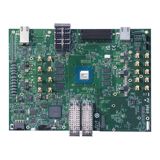
Summary of Contents for Intel altera Agilex 5 FPGA E 065B Series
- Page 1 ™ Agilex 5 FPGA E-Series 065B Premium Development Kit User Guide 814550 Online Version Send Feedback 2024.05.20...
-
Page 2: Table Of Contents
Contents Contents 1. Overview........................4 1.1. Block Diagram.......................5 1.2. Feature Summary....................6 1.3. Box Contents......................7 1.4. Recommended Operating Conditions................ 8 2. Getting Started....................... 9 ® 2.1. Quartus Prime Software and Driver Installation............9 2.2. Quick Start Guide....................9 2.3. Design Examples....................10 3. - Page 3 Contents A. Development Kit Components..................66 A.1. Board Overview....................66 A.2. System Management....................66 A.2.1. JTAG Master Sources................67 A.3. Power........................ 68 A.4. Clocks........................ 70 A.5. General Input/Output................... 71 A.6. Input and Output Components................73 A.6.1. Push Buttons...................73 A.6.2. Switches....................74 A.6.3. LEDs...................... 75 A.7.
-
Page 4: Overview
Altera or Intel. Altera and Intel customers are advised to obtain the latest version of device specifications before relying on any published information and before placing orders for products or services. -
Page 5: Block Diagram
1. Overview 814550 | 2024.05.20 Related Information Development Kit Components on page 66 1.1. Block Diagram Figure 2. Agilex 5 FPGA E-Series 065B Premium Development Kit Block Diagram Nios 2 Gb Flash QSPI Hyper DDR4 MAX 10 COMP Pin Header ASx4 2 Gb Button/... -
Page 6: Feature Summary
Active Serial (AS) x4 configuration mode support — 2 Gb flash for Avalon streaming interface x8 configuration mode — 2 Gb flash for AS x4 configuration mode ® — Built-in Intel FPGA Download Cable II for JTAG mode device programming • Programmable clock sources •... -
Page 7: Box Contents
1. Overview 814550 | 2024.05.20 • Communication ports — JTAG header — Micro USB onboard Intel FPGA Download Cable II • Buttons, switches, and LEDs — HPS reset push button — Four dedicated user push buttons — Four dedicated user DIP switches —... -
Page 8: Recommended Operating Conditions
1. Overview 814550 | 2024.05.20 1.4. Recommended Operating Conditions Table 2. Recommended Operating Conditions Operating Condition Range of Values Ambient operating temperature range 0⁰C to 35⁰C ICC load current 38 A ICC load transient percentage 204 A/us FPGA maximum power supported by active heat sink/fan 60 W When handling the board, it is important to observe static discharge precautions. -
Page 9: Getting Started
Altera or Intel. Altera and Intel customers are advised to obtain the latest version of device specifications before relying on any published information and before placing orders for products or services. -
Page 10: Design Examples
2. Getting Started 814550 | 2024.05.20 Related Information Agilex 5 FPGA E-Series 065B Premium Development Kit Website More information about the Agilex 5 FPGA E-Series 065B Premium Development Kit documentation, including the Quick Start Guide and development kit unboxing video. 2.3. -
Page 11: Development Kit Setup
Altera or Intel. Altera and Intel customers are advised to obtain the latest version of device specifications before relying on any published information and before placing orders for products or services. -
Page 12: Powering Up The Development Kit
3. Development Kit Setup 814550 | 2024.05.20 Switch Default Position Function SW21[1:4] OFF/OFF/OFF/OFF User defined switch: • ON—Sets the switch to low • OFF—Sets the switch to high SW24[1:4] ON/ON/ON/ON Connected to HSIO I/O for debugging purpose: • ON—Connects to ground (GND) •... -
Page 13: Restoring Board Qspi Flash U4 With The Default Factory Image
3. Development Kit Setup 814550 | 2024.05.20 1. Make sure SW27[3:1] are [off off off] (JTAG mode). 2. Open the Quartus Prime Programmer GUI, and click Auto Detect. 3. Right click on the FPGA device, and choose change file to use the GHRD image. 4. -
Page 14: Board Test System
Altera or Intel. Altera and Intel customers are advised to obtain the latest version of device specifications before relying on any published information and before placing orders for products or services. -
Page 15: Setting Up Bts Gui Running Environment
4. Board Test System 814550 | 2024.05.20 4.1. Setting Up BTS GUI Running Environment To run BTS GUI, including the Power Monitor and Clock Controller GUI, you must download and install Java runtime including OpenJDK and OpenJFX on your systems and set up the running environment. -
Page 16: Installing Quartus Prime Software
4. Board Test System 814550 | 2024.05.20 Note: The unzipped folder name of JRE is (for example, jdk-11.0.xx+x-jre ), and you must rename it to . The unzipped jdk-11.0.14+9-jre folder name of JFX is , and you must rename it to javafx-sdk-17.0.2 2. -
Page 17: Running The Bts Gui
4. Board Test System 814550 | 2024.05.20 4.1.5. Running the BTS GUI With the power to the board off, follow these steps. 1. Connect the micro-USB cable to your PC and the board. 2. Check the development board switches and jumpers are set according to your preferences. -
Page 18: Troubleshooting For Launching Bts
4. Board Test System 814550 | 2024.05.20 Figure 6. Linux Console of BTS Launching Note: or shell script checks the Java environment settings, copies necessary files, .bat and gives some prompts if the environment is not set up correctly. 4.2. Troubleshooting for Launching BTS No Available Serial Ports Figure 7. - Page 19 4. Board Test System 814550 | 2024.05.20 • Manufacturer = FTDI • Vendor ID = 0x403 • Product ID = 0x6010 or 0x6011 • Two consecutive serial ports number. For example, USB Serial Port (COM10) and USB Serial Port (COM11). If no valid UART ports are in the list, it may be due to UART driver is not installed properly.
- Page 20 4. Board Test System 814550 | 2024.05.20 Figure 9. UART Manufacturer Figure 10. UART VID/PID ™ Agilex 5 FPGA E-Series 065B Premium Development Kit User Guide Send Feedback...
- Page 21 4. Board Test System 814550 | 2024.05.20 No Response after Message Sent Figure 11. Failure of "sending msg is successful, but no response received" The issue roots that the UART does not work correctly, follow the check list below: 1. Check if the BTS is launched before the board is ready. 2.
-
Page 22: Bts Functionalities
4. Board Test System 814550 | 2024.05.20 4.3. BTS Functionalities This section describes each control in the BTS. 4.3.1. Diagnostic GUI The Diagnostic menu provides the functionality of checking the status of the devices. To trigger a basic board diagnostic, click the Start button. After it is completed, the color of the light indicates if the test is a pass or a fail. - Page 23 4. Board Test System 814550 | 2024.05.20 Figure 12. Diagnostic ™ Agilex 5 FPGA E-Series 065B Premium Development Kit User Guide Send Feedback...
-
Page 24: Clock Controller Gui
4. Board Test System 814550 | 2024.05.20 4.3.2. Clock Controller GUI The Clock Controller GUI can change the onboard programmable PLLs to a large range of customized frequency. Select the Clock icon on the BTS GUI to start the Clock Controller feature. - Page 25 4. Board Test System 814550 | 2024.05.20 4.3.2.1. Si5332 Clock Figure 14. The Si5332 Setting Page ™ Agilex 5 FPGA E-Series 065B Premium Development Kit User Guide Send Feedback...
- Page 26 4. Board Test System 814550 | 2024.05.20 • Default: Restores to factory default settings. • Read: Reads the current real-time frequency setting for the oscillator associated with the active tab. • Set: Sets the programmable oscillator frequency for the selected clock to the value in the OUTx output controls.
- Page 27 4. Board Test System 814550 | 2024.05.20 4.3.2.2. Si5518 Clock Figure 16. The Si5518 Setting Page ™ Agilex 5 FPGA E-Series 065B Premium Development Kit User Guide Send Feedback...
-
Page 28: Power Monitor Gui
4. Board Test System 814550 | 2024.05.20 • Status: Displays the current configured status. • Default: Restores to factory default settings. • Soft Reset: Reboots the device without downloading the firmware and frequency plan from the NVM. • Import: Imports configurable Si5518 firmware and user boot binary files, which are generated from the tool of the Skyworks* Clockbuilder Pro software. - Page 29 4. Board Test System 814550 | 2024.05.20 • Power Monitor • Temperature Monitor Figure 18. The Entry of Launching Power Application 4.3.3.1. Power Monitor The Power Monitor module reads the real-time data from power chips, for example, LTC7883. BTS supports 10 rails listed below. For detailed information, refer to the schematic document.
- Page 30 4. Board Test System 814550 | 2024.05.20 Figure 19. Power Monitor GUI—Power 4.3.3.2. Temperature Monitor The BTS can monitor the temperature and presents the data visually, including the historical data and real-time data. The board hardware is designed with a specialized temperature, and can monitor temperatures at four different locations on the board.
- Page 31 4. Board Test System 814550 | 2024.05.20 Figure 20. Power Monitor GUI—Temperature ™ Agilex 5 FPGA E-Series 065B Premium Development Kit User Guide Send Feedback...
-
Page 32: Max 10 Controller Gui
4. Board Test System 814550 | 2024.05.20 4.3.4. MAX 10 Controller GUI The Agilex 5 FPGA E-Series 065B Premium Development Kit provides you with a UART based controller to manage I/O devices and HPS card, as well as perform other system functions. - Page 33 4. Board Test System 814550 | 2024.05.20 • Main Board: Four user defined push buttons on the main board are listed in the table below. Type Switch Board Label Push Button SW17 USER_PB1 Push Button SW18 USER_PB2 Push Button SW19 USER_PB3 Push Button SW20...
- Page 34 4. Board Test System 814550 | 2024.05.20 Type Switch Board Label DIP Switch SW21.1 USER SW1 DIP Switch SW21.2 USER SW2 DIP Switch SW21.3 USER SW3 DIP Switch SW21.4 USER SW4 Figure 23. The Remote Control of User Switch MSEL All the user MSEL located on the main board are defined as follows: Type Switch...
- Page 35 4. Board Test System 814550 | 2024.05.20 Figure 24. The Remote Control of MSEL Si569-1V8 The control of Si569-1V8 targets for swapping the Si569 input frequency remotely. There are two input source frequencies: • 148.35 MHz (default) • 148.5 MHz ™...
- Page 36 4. Board Test System 814550 | 2024.05.20 Figure 25. The Remote Control of Si569-1V8 4.3.4.1.2. MISC LED Control You can use the BTS to control the user LEDs. Click on the LED icon to turn on and turn off the LED. The All button operates and reverses the states of all the LEDs. This function is useful to verify if the LED physical channel is okay or not.
- Page 37 4. Board Test System 814550 | 2024.05.20 Figure 26. The Control of MISC LED 4.3.4.2. Expansion Board Control BTS also extends its functionality to the HPS expansion boards. The Agilex 5 FPGA E- Series 065B Premium Development Kit has three types of HPS expansion boards: •...
- Page 38 4. Board Test System 814550 | 2024.05.20 Figure 27. The Control of Expansion Board 4.3.4.3. System Control You could power cycle the Agilex 5 FPGA E-Series using this tab. ™ Agilex 5 FPGA E-Series 065B Premium Development Kit User Guide Send Feedback...
- Page 39 4. Board Test System 814550 | 2024.05.20 Figure 28. The Control of System ™ Agilex 5 FPGA E-Series 065B Premium Development Kit User Guide Send Feedback...
-
Page 40: Agilex 5 Fpga E-Series Test Functionality
4. Board Test System 814550 | 2024.05.20 4.3.5. Agilex 5 FPGA E-Series Test Functionality Figure 29. The Entry of Launching Agilex Application 4.3.5.1. DDR4 Test The BTS provides a convenient and fast way to test DDR4 memory on the development kit board. The BTS automatically launches the test procedure if you select Configure with DDR4 COMP Design. - Page 41 4. Board Test System 814550 | 2024.05.20 Figure 30. DDR4 Test Entry ™ Agilex 5 FPGA E-Series 065B Premium Development Kit User Guide Send Feedback...
- Page 42 4. Board Test System 814550 | 2024.05.20 Figure 31. DDR4 Test Page The following sections describe controls on this tab. • Start: Initiates DDR4 memory transaction performance analysis. • Stop: Terminates transaction performance analysis. • Test Control — Test Mode: Infinite Read and Write (default), Single Read and Write. —...
- Page 43 4. Board Test System 814550 | 2024.05.20 4.3.5.2. HPS DDR4 Test The test flow of HPS DDR4 is the same as DDR4 test. Refer to the DDR4 Test section. Figure 32. HPS DDR4 Test Entry ™ Agilex 5 FPGA E-Series 065B Premium Development Kit User Guide Send Feedback...
- Page 44 4. Board Test System 814550 | 2024.05.20 Figure 33. HPS DDR4 Test Page Related Information DDR4 Test on page 40 ™ Agilex 5 FPGA E-Series 065B Premium Development Kit User Guide Send Feedback...
- Page 45 4. Board Test System 814550 | 2024.05.20 4.3.5.3. LPDDR4 Test BTS provides a design of testing DDR4 in low-power mode. To execute the test, select Configure with LPDDR4 COMP Design. Figure 34. LPDDR4 Test Entry ™ Agilex 5 FPGA E-Series 065B Premium Development Kit User Guide Send Feedback...
- Page 46 4. Board Test System 814550 | 2024.05.20 Figure 35. LPDDR4 Test Page ™ Agilex 5 FPGA E-Series 065B Premium Development Kit User Guide Send Feedback...
- Page 47 4. Board Test System 814550 | 2024.05.20 4.3.5.4. QSFP Test Select Configure with QSFP Design to launch the QSFP test application. The BTS automatically enables the specific application after downloading the design file ( .sof Figure 36. QSFP Test Entry ™...
- Page 48 4. Board Test System 814550 | 2024.05.20 • Data Type: The Data Type control specifies the type of data pattern contained in the transactions. Select the following available data types for analysis: — PRBS7: Pseudo-random 7-bit binary sequences. — PRBS15: Pseudo-random 15-bit binary sequences. —...
- Page 49 4. Board Test System 814550 | 2024.05.20 Figure 37. QSFP Test Page ™ Agilex 5 FPGA E-Series 065B Premium Development Kit User Guide Send Feedback...
- Page 50 4. Board Test System 814550 | 2024.05.20 4.3.5.5. SFP+ Test The SFP+ test shares the same test flow and test page with the QSFP test except the difference of the RTL design. Refer to the QSFP Test section for details. Figure 38.
- Page 51 4. Board Test System 814550 | 2024.05.20 Figure 39. SFP+ Test Page Related Information QSFP Test on page 47 ™ Agilex 5 FPGA E-Series 065B Premium Development Kit User Guide Send Feedback...
- Page 52 4. Board Test System 814550 | 2024.05.20 4.3.5.6. FMC+ Test The FMC+ test shares the same test flow and test page with the QSFP test except the difference of the RTL design. Refer to the QSFP Test section for details. Figure 40.
- Page 53 4. Board Test System 814550 | 2024.05.20 Figure 41. FMC+ Test Page Related Information QSFP Test on page 47 ™ Agilex 5 FPGA E-Series 065B Premium Development Kit User Guide Send Feedback...
- Page 54 4. Board Test System 814550 | 2024.05.20 4.3.5.7. SMA Test The SMA test shares the same test flow and test page with the QSFP test except the difference of the RTL design. Refer to the QSFP Test section for details. Figure 42.
- Page 55 4. Board Test System 814550 | 2024.05.20 Figure 43. SMA Test Page Related Information QSFP Test on page 47 ™ Agilex 5 FPGA E-Series 065B Premium Development Kit User Guide Send Feedback...
-
Page 56: Information Display
4. Board Test System 814550 | 2024.05.20 4.3.6. Information Display 4.3.6.1. Sys Info The Sys Info menu presents the basic system information of the development kit. • Dev Kit Name: The official development kit name. • Board Revision: The silicon version. •... - Page 57 4. Board Test System 814550 | 2024.05.20 Figure 45. Connection 4.3.6.3. The Bottom Status Bar The bottom information bar shows the status of the UART connection, the recognized Quartus Prime software version. • UART: Shows if the board is connected to BTS successfully. •...
- Page 58 4. Board Test System 814550 | 2024.05.20 Figure 46. Bottom Status Bar ™ Agilex 5 FPGA E-Series 065B Premium Development Kit User Guide Send Feedback...
-
Page 59: Development Kit Hardware And Configuration
Altera or Intel. Altera and Intel customers are advised to obtain the latest version of device specifications before relying on any published information and before placing orders for products or services. -
Page 60: Configuring The Fpga Device By Avalon Streaming Modes
5. Development Kit Hardware and Configuration 814550 | 2024.05.20 5.3. Configuring the FPGA Device by Avalon Streaming Modes 1. Set SW27 (or use BTS for remote control) to Avalon streaming interface x8 mode. Note: The default MAX 10 image and hardware design supports the Avalon streaming interface x8 configuration only. -
Page 61: Hps Expansion Board (Hps-Eb)
5. Development Kit Hardware and Configuration 814550 | 2024.05.20 5.4.1. HPS Expansion Board (HPS-EB) Figure 47. HPS Expansion Board (Top View) UART Connector User LED Connector Ethernet Connector Push Button 1. Plug HPS-EB in J11. 2. To test HPS Ethernet capability, connect HPS-EB’s RJ45 port J5 to the Internet. 3. -
Page 62: Hps Nand Board (Hps-Nb)
5. Development Kit Hardware and Configuration 814550 | 2024.05.20 5.4.2. HPS NAND Board (HPS-NB) Figure 48. HPS NAND Board (Top View) User LED UART Connector Ethernet Connector Push Button 1. Plug HPS-NB in J11. 2. To test HPS Ethernet capability, connect HPS-NB’s RJ45 port J5 to the Internet. 3. -
Page 63: Hps Test Board (Hps-Tb)
5. Development Kit Hardware and Configuration 814550 | 2024.05.20 5.4.3. HPS Test Board (HPS-TB) Figure 49. HPS Test Board (Top View) UART User LED Connector Ethernet Connector Push Button 1. Plug HPS-TB in J11. 2. To test HPS Ethernet capability, connect HPS-TB’s RJ45 port J5 to the Internet. 3. -
Page 64: Custom Projects For The Development Kit
Altera or Intel. Altera and Intel customers are advised to obtain the latest version of device specifications before relying on any published information and before placing orders for products or services. -
Page 65: Document Revision History For The Agilex 5 Fpga E-Series 065B Premium Development Kit User Guide
Altera or Intel. Altera and Intel customers are advised to obtain the latest version of device specifications before relying on any published information and before placing orders for products or services. -
Page 66: Development Kit Components
Altera or Intel. Altera and Intel customers are advised to obtain the latest version of device specifications before relying on any published information and before placing orders for products or services. -
Page 67: Jtag Master Sources
Table 7. JTAG Master Sources Schematic Signal Name Description JTAG header J2 for external Intel FPGA Download Cable. EXT_JTAG_TCK/TDO/TMS/TDI Input port J27 for embedded Intel FPGA Download Cable. FX2_Dp/n Mictor* 38-pin header on HPS Out of Box Experience (OOBE) card. -
Page 68: Power
A. Development Kit Components 814550 | 2024.05.20 A.3. Power Figure 51. Power Tree Power Sequence FPGA Recommendation: PWR_ON MAX10 Group0 Group1 Group2 Group3 Group4 The development kit power tree design are for the reference. SWITCH Scale power solution based on design requirements. 12V_IN MAX16545 12V_SYS... - Page 69 A. Development Kit Components 814550 | 2024.05.20 Figure 52. Power Sequence POWER IN 12V_IN POWER ON 12V_EARLY 12V_EARLY_PG 5V0_SYS 5V0_SYS_PG 3V3_SYS 3V3_SYS_PG 3V3_MAX 2V5_MAX 1V8_MAX POWER OK 1V2_MAX 3V3_USB 1V1_USB 3V3_Si5518A 1V8_Si5518A Group 0 12V_SYS PWRGD_G0 12V_HPS Group 1 FPGA_VCC VCC_HSSI PWRGD_G1 VCCERT_UX...
-
Page 70: Clocks
A. Development Kit Components 814550 | 2024.05.20 MAX 10 also shuts down significant power rails when temperature cross the acceptable range. A.4. Clocks Table 8. Onboard Clock Sources Source Signal Name Default I/O Standard Application Frequency 1 Hz LVCMOS 3.3 V 1PPS to FPGA 1PPS_3V3_SI5518_TO_FPGA 1 Hz... -
Page 71: General Input/Output
A. Development Kit Components 814550 | 2024.05.20 Figure 53. Clock Tree (50 MHz) MAX10_50M_CLK NIOS_CLK CFG_FLASH_1V8_CLK MAX10 USB_T_CLK A5ED065BB32A – Fabric AVSTx8_1V8_CLK AVSTx8_CLK OSC_CLK_1 Si5518 (125 MHz) 1PPS_GRAND_MASTER_LOOPBACK (LVCMOS 3.3V) OUT0n QSFP1_RCVD_REFCLK 1PPS_3V3_SI5518_TO_FPGA (LVCMOS 3.3V) OUT0p IN3n PTP_SAMPLE_CLK_250M (250 MHz LVDS) QSFP1_REFCLK 1PPS SMA IN OUT1... - Page 72 A. Development Kit Components 814550 | 2024.05.20 Schematic Signal Name Description Spread spectrum enable for SI5332A (U411). SI5332A_1_IN3 Output enable pin for SI5332A (U411). SI5332A_1_IN4 Output frequency select pin for SI5332A (U411) OUT2. SI5332A_1_IN5 • High: 199.95 MHz • Low: 116.625 MHz Clock in SEL0 for SI5332A (U412).
-
Page 73: Input And Output Components
A. Development Kit Components 814550 | 2024.05.20 Schematic Signal Name Description Output for LED4. FPGA_USER_LED4_1V1 Interrupt pin status output for SI5518A or chip select of secondary SPI FPGA_1V1_SI5518A_GPIO0 port. Loss of lock status output for DSPLL A or SDIO of secondary SPI port. FPGA_1V1_SI5518A_GPIO1 Output enable control pin or SCLK of secondary SPI port. -
Page 74: Switches
OFF to enable HPS JTAG chain SW16.3 • ON to select embedded Intel FPGA Download USB_MAX_JTAG_SEL Cable II • OFF to select external Intel FPGA Download Cable II dongle SW16.4 • ON to bypass FMC JTAG chain SW_FMC_JTAG_BYPASS • OFF to enable FMC JTAG chain SW21.1... -
Page 75: Leds
A. Development Kit Components 814550 | 2024.05.20 A.6.3. LEDs The Agilex 5 FPGA E-Series 065B Premium Development Kit provides various LEDs for indicating board status information. Table 13. LEDs Board Reference Schematic Signal Name Description Green when the MAX 10 configuration done. MAX10 CONF DONE Green when the FPGA configuration done. -
Page 76: Communication Interfaces
A. Development Kit Components 814550 | 2024.05.20 FPGA Dedicated External Memory Interface (DDR4) The Agilex 5 FPGA E-Series 065B Premium Development Kit provides 8GB DDR4 x40 interface, which comprises three DDR4 x16 components. This gives 32-bits data plus 8-bits ECC, which are connected to bank 2B. It targets up to 2400 Mbps. Three Micron MT40A2G16TBB-062E:F are soldered down on the development kit. -
Page 77: Sfp
A. Development Kit Components 814550 | 2024.05.20 Schematic Signal Name Description C data FPGA_3V3_SDA Transceiver TX QSFP2_TX[0:3]_P/N Transceiver RX QSFP2_RX[0:3]_P/N A.8.2. SFP+ The Agilex 5 FPGA E-Series 065B Premium Development Kit includes 2x SFP+ ports with connected to transceiver bank 4A CH2 (supports PMA direct) and CH3 (supports 10/25 GE or PMA direct). -
Page 78: Ethernet
A. Development Kit Components 814550 | 2024.05.20 A.8.3. Ethernet The Agilex 5 FPGA E-Series 065B Premium Development Kit supports three Ethernet configurations. Table 18. Ethernet Configuration Index Interface Configuration Supported Rates External PHY Connector Reference RGMII (via HPS pins) 10M/100M/1G Marvell* 88E1512 J5 (on HPS card) RGMII (via FPGA HVIO... -
Page 79: Fmc
A. Development Kit Components 814550 | 2024.05.20 Table 20. SGMII via FPGA XCVR Schematic Signal Name Description SGMII transmit data 88E2110_SGMII_ENET1_TXP/N SGMII receive data 88E2110_SGMII_ENET1_RXP/N Management data clock reference 88E2210_ENET1_MDC Management data 88E2210_ENET1_MDIO 88E1512 reset pin 88E2110_ENET1_RESETN Interrupt output pin 88E2210_ENET1_INTN A.8.4. -
Page 80: Mipi
A. Development Kit Components 814550 | 2024.05.20 Schematic Signal Name Description Remark Optional Refclk driven from the FPGA Connect to HSIO bank 3B (1.2 V) FMC_REFCLK_C2M_P/N to the FMC card for synchronization Optional Refclk driven from the FMC Connect to HSIO bank 3B (1.2 V) FMC_REFCLK_M2C_P/N card to the FPGA for synchronization FMC card present signal... -
Page 81: Hps Io48 Interface
A. Development Kit Components 814550 | 2024.05.20 A.8.7. HPS IO48 Interface The Agilex 5 FPGA E-Series 065B Premium Development Kit connects the 48 HPS I/Os to ADM connector (J11) for the HPS Out of Box Experience (OOBE) card installation. This HPS OOBE card provides the HPS with USB, UART, Ethernet, SD card, I C, and JTAG accessibility. -
Page 82: Expansion Boards
A. Development Kit Components 814550 | 2024.05.20 Figure 54. C Serial Bus MAX_I2C_SDA/SCL U401 Header M24128-BWMN6TP MAX31730ATC+ MAX16545 MAX16545 LTC7883AY LTC7883AY EEPROM (FRUID/CFG) Temp Sensor 0X57/0X5F OX1C 0X40 0X42 Global: 0X5A & Global: 0X5A & FPGA_3V3_SVID_SDA/SCL 12V_EARLY 12V_SYS 0X5B 0X5B CHA: 0X74 CHA: 0X47 CHB:0X75... - Page 83 A. Development Kit Components 814550 | 2024.05.20 IO48 Interface Type Signal Name I/O Direction IOA06 EMAC2 PPSTRIG2 IOA07 MDIO2 MDIO IOA08 MDIO2 IOA09 I3C1 IOA10 I3C1 IOA11 LED1 IO10 IOA12 LED2 IO11 IOA13 USB1 IOA14 USB1 STEP IOA15 USB1 IOA16 USB1 DATA0 IOA17...
-
Page 84: Connectors And Headers
A. Development Kit Components 814550 | 2024.05.20 IO48 Interface Type Signal Name I/O Direction IOB16 EMAC2 RX_CTL IOB17 EMAC2 TXD0 IOB18 EMAC2 TXD1 IOB19 EMAC2 RXD0 IOB20 EMAC2 RXD1 IOB21 EMAC2 TXD2 IOB22 EMAC2 TXD3 IOB23 EMAC2 RXD2 IOB24 EMAC2 RXD3 A.10. - Page 85 A. Development Kit Components 814550 | 2024.05.20 Board Reference Description Part Number HSIO bank SMA connector for 1PPS_IN1 (or LTI-SASF546-P26-X1 (Lighthorse Technology) LVDS_SMA_RXN) HSIO bank SMA connector for 1PPS_IN2 (or LTI-SASF546-P26-X1 (Lighthorse Technology) LVDS_SMA_RXP) XCVR bank SMA connector for TX1_P/N LTI-SASF546-P26-X1 (Lighthorse Technology) XCVR bank SMA connector for TX2_P/N LTI-SASF546-P26-X1 (Lighthorse Technology)
-
Page 86: Additional Information
Altera or Intel. Altera and Intel customers are advised to obtain the latest version of device specifications before relying on any published information and before placing orders for products or services. -
Page 87: Safety Warnings
B. Additional Information 814550 | 2024.05.20 B.1.1. Safety Warnings Power Supply Hazardous Voltage AC mains voltages are present within the power supply assembly. No user serviceable parts are present inside the power supply. Power Connect and Disconnect The AC power supply cord is the primary disconnect device from mains (AC power) and used to remove all DC power from the board/system. -
Page 88: Safety Cautions
B. Additional Information 814550 | 2024.05.20 Power Cord Requirements The plug on the power cord must be a grounding-type male plug designed for use in your region. It must have certification marks showing certification by an agency in your region. The connector that plugs into the appliance inlet of the power supply must be an IEC 320, sheet C13, female connector. - Page 89 B. Additional Information 814550 | 2024.05.20 Cooling Requirements Maintain a minimum clearance area of 5 centimeters (2 inches) around the side, front and back of the board for cooling purposes. Do not block power supply ventilation holes and fan. Electro-Magnetic Interference (EMI) This equipment has not been tested for compliance with emission limits of FCC and similar international regulations.
- Page 90 Failure to use wrist straps can damage components within the system. Attention: Please return this product to Intel for proper disposition. If it is not returned, refer to local environmental regulations for proper recycling. Do not dispose of this product in unsorted municipal waste.
-
Page 91: Compliance Information
B. Additional Information 814550 | 2024.05.20 Please return this product to Intel for proper disposition. If it is not returned, refer to local environmental regulations for proper recycling. Do not dispose of product in unsorted municipal waste. B.2. Compliance Information...
Need help?
Do you have a question about the altera Agilex 5 FPGA E 065B Series and is the answer not in the manual?
Questions and answers