
Related Manuals for Intel Arria 10 FPGA


Summary of Contents for Intel Arria 10 FPGA
- Page 1 ® ® Intel Arria 10 FPGA Development Kit User Guide 683526 Online Version Send Feedback 2023.07.12 UG-20007...
-
Page 2: Table Of Contents
Contents Contents ® ® 1. Intel Arria 10 FPGA Development Kit Overview............4 1.1. General Description....................5 1.2. Recommended Operating Conditions................ 6 1.3. Handling the Board....................7 2. Getting Started....................... 8 2.1. Installing the Subscription Edition Software...............8 2.1.1. Activating Your License................8 2.2. - Page 3 6.9.2. Power Measurement................107 6.10. Daughtercards....................108 6.10.1. External Memory Interface..............109 A. Additional Information....................117 A.1. Document Revision History for the Intel Arria 10 FPGA Development Kit User Guide..117 A.2. Compliance and Conformity Statements..............118 A.2.1. CE EMI Conformity Caution..............118 ®...
-
Page 4: Intel ® Arria ® 10 Fpga Development Kit Overview
Intel's standard warranty, but reserves the right to make changes to any 9001:2015 products and services at any time without notice. Intel assumes no responsibility or liability arising out of the Registered application or use of any information, product, or service described herein except as expressly agreed to in writing by Intel. -
Page 5: General Description
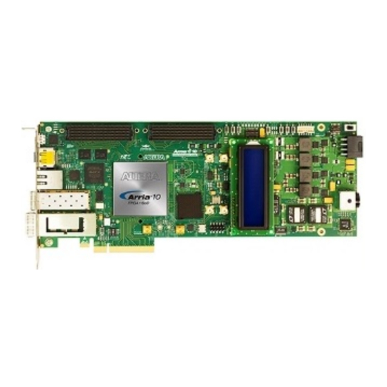
® ® 1. Intel Arria 10 FPGA Development Kit Overview 683526 | 2023.07.12 1.1. General Description Figure 1. Arria 10 GX Block Diagram Micro- Altera Altera MAX II FMCA FMCB On-Board USB Blaster & USB Interface JTAG Chain HiLO External... -
Page 6: Recommended Operating Conditions
® ® 1. Intel Arria 10 FPGA Development Kit Overview 683526 | 2023.07.12 Figure 2. Overview of the Development Board Features (ES Edition) FMCA (J1) FMCB (J2) LTPowerPlay interface Arria 10 Connector (J24) Clock In/Out FPGA (U28) Power Switch SMA (J6, J7) User Dipswitch... -
Page 7: Handling The Board
® ® 1. Intel Arria 10 FPGA Development Kit Overview 683526 | 2023.07.12 1.3. Handling the Board When handling the board, it is important to observe static discharge precautions. Caution: Without proper anti-static handling, the board can be damaged. Therefore, use anti- static handling precautions when touching the board. -
Page 8: Getting Started
Intel's standard warranty, but reserves the right to make changes to any 9001:2015 products and services at any time without notice. Intel assumes no responsibility or liability arising out of the Registered application or use of any information, product, or service described herein except as expressly agreed to in writing by Intel. -
Page 9: Development Kit Package
• myAltera Account Sign In web page 2.2. Development Kit Package 1. Download the Arria 10 FPGA Development Kit package zip file available at the Intel website. 2. Extract the contents of the zip file to your hard drive. The development kit directory structure is shown in the following figure. - Page 10 Information page of the Altera website, locate the table entry for your configuration and click the link to access the instructions. Related Information Altera Programming Cable Driver Information Click on the link for your operating system. ® ® Intel Arria 10 FPGA Development Kit User Guide Send Feedback...
-
Page 11: Development Board Setup
Intel's standard warranty, but reserves the right to make changes to any 9001:2015 products and services at any time without notice. Intel assumes no responsibility or liability arising out of the Registered application or use of any information, product, or service described herein except as expressly agreed to in writing by Intel. -
Page 12: Default Switch And Jumper Settings
Default Switch Settings on the Bottom ARRIA 10 MSEL0 MAX V MSEL1 FMCA MSEL2 FMCB VIDEN CLK_SEL CLK_EN Si516_FS FACTORY RZQ_B2K 1. Set DIP switch bank (SW3) to match the following table. ® ® Intel Arria 10 FPGA Development Kit User Guide Send Feedback... - Page 13 ON for MSEL2 = 0; for FPP standard mode VIDEN OFF for enabling for the Smart Voltage ID (SmartVID) VID_EN feature 5. Set DIP switch bank (SW6) to match the following table. ® ® Intel Arria 10 FPGA Development Kit User Guide Send Feedback...
- Page 14 OFF to load user image #1 from flash RZQ_B2K ON for setting RZQ resistor of Bank 2K to 99.17 ohm OFF for setting RZQ resistor of Bank 2K to 240 ohm ® ® Intel Arria 10 FPGA Development Kit User Guide Send Feedback...
-
Page 15: Default Switch And Resistor Settings
Default Switch Settings on the Bottom ARRIA 10 MSEL0 MAX V MSEL1 FMCA MSEL2 FMCB VIDEN CLK_SEL CLK_EN Si516_FS FACTORY RZQ_B2K 1. Set DIP switch bank (SW3) to match the following table. ® ® Intel Arria 10 FPGA Development Kit User Guide Send Feedback... - Page 16 ON for MSEL2 = 0; for FPP standard mode VIDEN OFF for enabling for the Smart Voltage ID (SmartVID) VID_EN feature 5. Set DIP switch bank (SW6) to match the following table. ® ® Intel Arria 10 FPGA Development Kit User Guide Send Feedback...
- Page 17 OFF to load user image #1 from flash RZQ_B2K ON for setting RZQ resistor of Bank 2K to 99.17 ohm OFF for setting RZQ resistor of Bank 2K to 240 ohm ® ® Intel Arria 10 FPGA Development Kit User Guide Send Feedback...
-
Page 18: Factory Reset
"BoardTestSystem.exe" to open the GUI. 4. Select "Restore -> Factory Restore". Figure 9. Arria 10 FPGA Board Test System Factory Restore Select 5. Set the correct board information and then click restore. The restore process takes about 10 minutes. - Page 19 683526 | 2023.07.12 Figure 10. Factory Restore Window Related Information • Board Update Portal on page 52 • Using the Board Update Portal to Update User Designs on page 54 ® ® Intel Arria 10 FPGA Development Kit User Guide Send Feedback...
-
Page 20: Board Test System
Intel's standard warranty, but reserves the right to make changes to any 9001:2015 products and services at any time without notice. Intel assumes no responsibility or liability arising out of the Registered application or use of any information, product, or service described herein except as expressly agreed to in writing by Intel. - Page 21 II Embedded Logic Analyzer. Because the BTS is designed based on the Quartus Programmer and System Console, be sure to close other applications before you use the BTS application. ® ® Intel Arria 10 FPGA Development Kit User Guide Send Feedback...
-
Page 22: Preparing The Board
The BTS will pick up the Quartus Programmer to configure the FPGA device on your development kit. Make sure the Quartus Prime software you are using is the version supporting the FPGA silicon on the board. ® ® Intel Arria 10 FPGA Development Kit User Guide Send Feedback... -
Page 23: Version Selector
Silicon Version. Select the silicon version of the Arria 10 device that is installed on your board. Figure 12. Configure Tab Version Selector Option Figure 13. Version Selector ® ® Intel Arria 10 FPGA Development Kit User Guide Send Feedback... - Page 24 Board Serial Number Sticker Table 12. Serial Number to Arria 10 Silicon Revision Serial Number Arria 10 Silicon Revision 10APCIe000[< 0332] 10APCIe000[0332 – 0383] PRD-1 10APCIe000[0500 – 0999] 10APCIe000[1000+] ® ® Intel Arria 10 FPGA Development Kit User Guide Send Feedback...
-
Page 25: Using The Board Test System
If you use the Quartus Programmer for configuration, rather than the Board Test System GUI, you may need to restart the GUI. ® ® Intel Arria 10 FPGA Development Kit User Guide Send Feedback... -
Page 26: The System Info Tab
Allows you to view and change the current register values, which take effect immediately: System Reset (SRST) — Write only. Click to reset the FPGA. Page Select Override (PSO) — Read/Write continued... ® ® Intel Arria 10 FPGA Development Kit User Guide Send Feedback... - Page 27 MAX Ver: Indicates the version of MAX V code currently running on the board. JTAG Chain Shows all the devices currently in the JTAG chain. Qsys Memory Map Shows the memory map of the Qsys system on your board. ® ® Intel Arria 10 FPGA Development Kit User Guide Send Feedback...
-
Page 28: The Gpio Tab
Push Button Switches Read-only control displays the current state of the board user push buttons. Press a push button on the board to see the graphical display change accordingly. ® ® Intel Arria 10 FPGA Development Kit User Guide Send Feedback... -
Page 29: The Flash Tab
Updates the memory table, displaying the CFI ROM table contents from the flash device. Increment Test Starts an incrementing data pattern test to flash memory, limited to the 512 K test system scratch page. continued... ® ® Intel Arria 10 FPGA Development Kit User Guide Send Feedback... - Page 30 Executes the flash device’s reset command and updates the memory table displayed on the Flash tab. Erase Erases flash memory. Flash Memory Map Displays the flash memory map for the development board. ® ® Intel Arria 10 FPGA Development Kit User Guide Send Feedback...
-
Page 31: The Xcvr Tab
Details—Shows the PLL lock and pattern sync status: Port Allows you to specify which interface to test. The following port tests are available: continued... ® ® Intel Arria 10 FPGA Development Kit User Guide Send Feedback... - Page 32 Note: Always click Clear before Start. Stop—Terminates transaction performance analysis. TX and RX performance bars—Show the percentage of maximum theoretical data rate that the requested transactions are able to achieve. ® ® Intel Arria 10 FPGA Development Kit User Guide Send Feedback...
- Page 33 4. Board Test System 683526 | 2023.07.12 Figure 20. Set PMA Values Window ® ® Intel Arria 10 FPGA Development Kit User Guide Send Feedback...
-
Page 34: The Pcie Tab
PLL lock—Shows the PLL locked or unlocked state. Pattern sync—Shows the pattern synced or not synced state. The pattern is considered synced when the start of the data sequence is detected. continued... ® ® Intel Arria 10 FPGA Development Kit User Guide Send Feedback... - Page 35 Insert Error is only enabled during transaction performance analysis. • Clear—Resets the Detected errors and Inserted errors counters to zeroes. Loopback Start—Initiates the selected ports transaction performance analysis. continued... ® ® Intel Arria 10 FPGA Development Kit User Guide Send Feedback...
- Page 36 Note: Always click Clear before Start. Stop—Terminates transaction performance analysis. TX and RX performance bars—Show the percentage of maximum theoretical data rate that the requested transactions are able to achieve. ® ® Intel Arria 10 FPGA Development Kit User Guide Send Feedback...
-
Page 37: The Fmc A Tab
PLL lock—Shows the PLL locked or unlocked state. Pattern sync—Shows the pattern synced or not synced state. The pattern is considered synced when the start of the data sequence is detected. continued... ® ® Intel Arria 10 FPGA Development Kit User Guide Send Feedback... - Page 38 HF—Selects highest frequency divide-by-2 data pattern 10101010. • LF—Selects lowest frequency divide by 33 data pattern. Error Control Displays data errors detected during analysis and allows you to insert errors: continued... ® ® Intel Arria 10 FPGA Development Kit User Guide Send Feedback...
- Page 39 Note: Always click Clear before Start. Stop—Terminates transaction performance analysis. TX and RX performance bars—Show the percentage of maximum theoretical data rate that the requested transactions are able to achieve. ® ® Intel Arria 10 FPGA Development Kit User Guide Send Feedback...
-
Page 40: The Fmc B Tab
PLL lock—Shows the PLL locked or unlocked state. Pattern sync—Shows the pattern synced or not synced state. The pattern is considered synced when the start of the data sequence is detected. continued... ® ® Intel Arria 10 FPGA Development Kit User Guide Send Feedback... - Page 41 HF—Selects highest frequency divide-by-2 data pattern 10101010. • LF—Selects lowest frequency divide by 33 data pattern. Error Control Displays data errors detected during analysis and allows you to insert errors: continued... ® ® Intel Arria 10 FPGA Development Kit User Guide Send Feedback...
- Page 42 Note: Always click Clear before Start. Stop—Terminates transaction performance analysis. TX and RX performance bars—Show the percentage of maximum theoretical data rate that the requested transactions are able to achieve. ® ® Intel Arria 10 FPGA Development Kit User Guide Send Feedback...
-
Page 43: The Ddr3 Tab
136512 Mbps or 17064 MBps. Error Control This control displays data errors detected during analysis and allows you to insert errors: continued... ® ® Intel Arria 10 FPGA Development Kit User Guide Send Feedback... - Page 44 Clear—Resets the Detected errors and Inserted errors counters to zeroes. Number of Addresses to Write and Read Determines the number of addresses to use in each iteration of reads and writes. ® ® Intel Arria 10 FPGA Development Kit User Guide Send Feedback...
-
Page 45: The Ddr4 Tab
136512 Mbps or 17064 MBps. Error Control This control displays data errors detected during analysis and allows you to insert errors: continued... ® ® Intel Arria 10 FPGA Development Kit User Guide Send Feedback... - Page 46 Clear—Resets the Detected errors and Inserted errors counters to zeroes. Number of Addresses to Write and Read Determines the number of addresses to use in each iteration of reads and writes. ® ® Intel Arria 10 FPGA Development Kit User Guide Send Feedback...
-
Page 47: The Power Monitor
Test Settings Displays the following controls: Power Rail—Indicates the currently-selected power rail. After selecting the desired rail, click Reset to refresh the screen with updated board readings. continued... ® ® Intel Arria 10 FPGA Development Kit User Guide Send Feedback... - Page 48 General Information Displays MAX V version and current temperature of the FPGA and board. Reset Clears the graph, resets the minimum and maximum values, and restarts the Power Monitor. ® ® Intel Arria 10 FPGA Development Kit User Guide Send Feedback...
-
Page 49: The Clock Control
810 MHz with eight digits of precision to the right of the decimal point. For example, 421.31259873 is possible within 100 parts per million (ppm). The Target frequency control works in conjunction with the Set New Freq control. continued... ® ® Intel Arria 10 FPGA Development Kit User Guide Send Feedback... - Page 50 Each tab allows for separate control. The Si5338 is capable of synthesizing four independent user-programmable clock frequencies up to 350 MHz and select frequencies up to 710 MHz. Figure 28. Si5338 (U26) Tab ® ® Intel Arria 10 FPGA Development Kit User Guide Send Feedback...
- Page 51 You might see glitches on the clock during this time. Altera recommends resetting the FPGA logic after changing frequencies. Import Reg Map Import register map file generated from Silicon Laboratories ClockBuilder Desktop. ® ® Intel Arria 10 FPGA Development Kit User Guide Send Feedback...
-
Page 52: Board Update Portal
Intel's standard warranty, but reserves the right to make changes to any 9001:2015 products and services at any time without notice. Intel assumes no responsibility or liability arising out of the Registered application or use of any information, product, or service described herein except as expressly agreed to in writing by Intel. -
Page 53: Connecting To The Board Update Portal Web Page
You can also navigate directly to the Arria 10 GX FPGA Development Kit page of the Altera website to determine if you have the latest kit software. Related Information • Quartus Prime Software Page • Arria 10 GX FPGA Development Kit Web Page ® ® Intel Arria 10 FPGA Development Kit User Guide Send Feedback... -
Page 54: Using The Board Update Portal To Update User Designs
If you do overwrite the factory image, you can restore it by following the instructions in the “Factory Reset” section. Related Information Factory Reset on page 18 ® ® Intel Arria 10 FPGA Development Kit User Guide Send Feedback... -
Page 55: Board Components
Intel's standard warranty, but reserves the right to make changes to any 9001:2015 products and services at any time without notice. Intel assumes no responsibility or liability arising out of the Registered application or use of any information, product, or service described herein except as expressly agreed to in writing by Intel. - Page 56 FACTORY signal command sent at power up. This switch is located at the bottom of the board. CPU reset push button The default reset for the FPGA logic. continued... ® ® Intel Arria 10 FPGA Development Kit User Guide Send Feedback...
- Page 57 FS=1: 148.50 MHz Programmable oscillator Si570 programmable oscillator by the clock control GUI. Default is 100 MHz. 125.0-MHz oscillator 125.0-MHz voltage controlled crystal oscillator for the Ethernet interface.. continued... ® ® Intel Arria 10 FPGA Development Kit User Guide Send Feedback...
- Page 58 Made of gold-plated edge fingers for up to ×8 signaling in either Gen1, Gen2, or Gen3 mode. J1, J2 FMC Port FPGA mezzanine card ports A and B. continued... ® ® Intel Arria 10 FPGA Development Kit User Guide Send Feedback...
-
Page 59: Max V Cpld System Controller
• FPGA configuration from flash memory • Power consumption monitoring • Temperature monitoring • Fan control • Control registers for clocks • Control registers for remote update system ® ® Intel Arria 10 FPGA Development Kit User Guide Send Feedback... - Page 60 FM address bus FM_A11 1.8 V FM address bus FM_A12 1.8 V FM address bus FM_A13 1.8 V FM address bus FM_A14 1.8 V FM address bus continued... ® ® Intel Arria 10 FPGA Development Kit User Guide Send Feedback...
- Page 61 FM data bus FM_D20 1.8 V FM data bus FM_D21 1.8 V FM data bus FM_D22 1.8 V FM data bus FM_D23 1.8 V FM data bus continued... ® ® Intel Arria 10 FPGA Development Kit User Guide Send Feedback...
- Page 62 FPGA configuration data FPGA_CONFIG_D15 1.8 V FPGA configuration data FPGA_CONFIG_D16 1.8 V FPGA configuration data FPGA_CONFIG_D17 1.8 V FPGA configuration data FPGA_CONFIG_D18 1.8 V FPGA configuration data continued... ® ® Intel Arria 10 FPGA Development Kit User Guide Send Feedback...
- Page 63 MAX5_CLK 1.8 V MAX V Clock MAX5_CSN 1.8 V MAX V chip select MAX5_OEN 1.8 V MAX V output enable MAX5_WEN 1.8 V MAX V Write enable continued... ® ® Intel Arria 10 FPGA Development Kit User Guide Send Feedback...
- Page 64 2.5 V SPI Interface Serial Data SENSE_SMB_CLK 2.5 V C Interface Clock SENSE_SMB_DATA 2.5 V C Interface Data SI516_FS 2.5 V Silicon Labs SI516 Clock Device Frequency Select continued... ® ® Intel Arria 10 FPGA Development Kit User Guide Send Feedback...
- Page 65 On-board USB-Blaster II interface (reserved for future use) USB_CFG14 1.8 V On-board USB-Blaster II interface (reserved for future use) USB_M5_CLK 1.8 V On-board USB-Blaster II interface clock continued... ® ® Intel Arria 10 FPGA Development Kit User Guide Send Feedback...
-
Page 66: Fpga Configuration
Schematic Signal Name I/O Standard MAX_ERROR 2.5 V MAX_LOAD 2.5 V MAX_CONF_DONE 2.5 V FMCA_TX_LED 1.8 V FMCA_RX_LED 1.8 V PGM_LED0 2.5 V PGM_LED1 2.5 V PGM_LED2 2.5 V continued... ® ® Intel Arria 10 FPGA Development Kit User Guide Send Feedback... - Page 67 I/O Standard FMCA_PRSNTn 1.8 V FMCB_TX_LED 1.8 V FMCB_RX_LED 1.8 V FMCB_PRSNTn 1.8 V PCIE_LED_X1 1.8 V PCIE_LED_X4 1.8 V PCIE_LED_X8 1.8 V PCIE_LED_G2 1.8 V PCIE_LED_G3 1.8 V ® ® Intel Arria 10 FPGA Development Kit User Guide Send Feedback...
-
Page 68: User Input/Output
The Arria 10 GX FPGA development board includes a set of eight pairs user-defined LEDs. The LEDs illuminate when a logic 0 is driven, and turns off when a logic 1 is driven. There are no board-specific functions for these LEDs. ® ® Intel Arria 10 FPGA Development Kit User Guide Send Feedback... - Page 69 1.8 V USER_LED_G7 1.8 V USER_LED_R0 1.8 V USER_LED_R1 1.8 V USER_LED_R2 1.8 V USER_LED_R3 1.8 V USER_LED_R4 1.8 V USER_LED_R5 1.8 V USER_LED_R6 1.8 V USER_LED_R7 1.8 V ® ® Intel Arria 10 FPGA Development Kit User Guide Send Feedback...
-
Page 70: Character Lcd
1.8 V SPI slave select (only used in SPI mode) DISP_SPISS I2C_SCL_DISP AW33 1.8 V C LCD serial clock DISP_I2C_SCL I2C_SDA_DISP AY34 1.8 V C LCD serial data DISP_I2C_SDA ® ® Intel Arria 10 FPGA Development Kit User Guide Send Feedback... -
Page 71: Displayport
Differential I/O DP_ML_LANE_CP2 AH44 High Speed Lane 2 (positive) Differential I/O DP_ML_LANE_CP3 AF44 High Speed Lane 3 (positive) Differential I/O DP_RTN AL33 High Speed Return for power Differential I/O ® ® Intel Arria 10 FPGA Development Kit User Guide Send Feedback... -
Page 72: Sdi Video Input/Output Ports
SDI Video Input Interface Pin Assignments, Schematic Signal Names, and Functions Board Reference Schematic Signal Name FPGA Pin Number I/O Standard AGCN — — AGXP — — MF0_BYPASS AW32 1.8 V continued... ® ® Intel Arria 10 FPGA Development Kit User Guide Send Feedback... - Page 73 — — MODE_SEL — — MUTEREF — — SDI_EQIN_N1 — — SDI_EQIN_P1 — — SDO_N / SDI_RX_N High Speed Differential I/O SDO_P / SDI_RX_P High Speed Differential I/O ® ® Intel Arria 10 FPGA Development Kit User Guide Send Feedback...
-
Page 74: Clock Circuitry
1.8 V LVDS AN38 PCIE_OB_REFCLK_N 133.33 MHz 1.8 V LVDS EMI reference CLK_EMI_P clocks 1.8 V LVDS CLK_EMI_N 644.53125 MHz 1.8 V LVDS QSFP reference REFCLK_QSFP_P clocks continued... ® ® Intel Arria 10 FPGA Development Kit User Guide Send Feedback... -
Page 75: Off-Board Clock I/O
The output clocks can be programmed to different levels and I/O standards according to the FPGA device’s specification. Table 28. Off-Board Clock Inputs Source Schematic Signal Name I/O Standard Arria 10 FPGA Pin Description Number 2.5 V SMA clock input CLKIN_SMA Table 29. -
Page 76: Components And Interfaces
I/O Standard Description PCIE_EDGE_PERS BC30 1.8 V Reset PCIE_EDGE_REFC AL38 LVDS Motherboard reference clock LK_N PCIE_EDGE_REFC AL37 LVDS Motherboard reference clock LK_P PCIE_EDGE_SMBC BD29 1.8 V SMB clock continued... ® ® Intel Arria 10 FPGA Development Kit User Guide Send Feedback... - Page 77 Receive bus Differential I/O PCIE_TX_CN0 BB43 High Speed Transmit bus Differential I/O PCIE_TX_CN1 BA41 High Speed Transmit bus Differential I/O PCIE_TX_CN2 AY43 High Speed Transmit bus Differential I/O continued... ® ® Intel Arria 10 FPGA Development Kit User Guide Send Feedback...
- Page 78 High Speed Transmit bus Differential I/O PCIE_TX_CP6 AT44 High Speed Transmit bus Differential I/O PCIE_TX_CP7 AR42 High Speed Transmit bus Differential I/O PCIE_WAKEN_R AY29 1.8 V Wake signal ® ® Intel Arria 10 FPGA Development Kit User Guide Send Feedback...
-
Page 79: 10/100/1000 Ethernet Phy
Figure 33. SGMII Interface between FPGA (MAC) and Marvell 88E1111 PHY RJ45 + MDI Interface SGMII TX/RX Marvell 10/100/1000 Phy Arria 10 FPGA Magnetics Table 31. Ethernet PHY Pin Assignments, Signal Names and Functions Board Reference Schematic Signal FPGA Pin Number... - Page 80 SGMII transmit channel ENET_XTAL_25MH — 2.5 V 25-MHz RGMII transmit clock MDI_N0 — Media dependent interface MDI_N1 — MDI_N2 — MDI_N3 — MDI_P0 — MDI_P1 — MDI_P2 — MDI_P3 — ® ® Intel Arria 10 FPGA Development Kit User Guide Send Feedback...
-
Page 81: Hilo External Memory Interface
MEM_ADDR_CMD16 1.5 V MEM_ADDR_CMD17 1.5 V MEM_ADDR_CMD18 1.5 V MEM_ADDR_CMD19 1.5 V MEM_ADDR_CMD20 1.5 V MEM_ADDR_CMD21 1.5 V MEM_ADDR_CMD22 1.5 V MEM_ADDR_CMD23 1.5 V MEM_ADDR_CMD24 1.5 V continued... ® ® Intel Arria 10 FPGA Development Kit User Guide Send Feedback... - Page 82 MEM_DQA1 1.5 V MEM_DQA2 1.5 V MEM_DQA3 1.5 V MEM_DQA4 1.5 V MEM_DQA5 1.5 V MEM_DQA6 1.5 V MEM_DQA7 1.5 V MEM_DQA8 1.5 V MEM_DQA9 1.5 V continued... ® ® Intel Arria 10 FPGA Development Kit User Guide Send Feedback...
- Page 83 AD32 1.5 V MEM_DQB6 AD33 1.5 V MEM_DQB7 AA30 1.5 V MEM_DQB8 AE31 1.5 V MEM_DQB9 AE32 1.5 V MEM_DQB10 AE30 1.5 V MEM_DQB11 AF30 1.5 V continued... ® ® Intel Arria 10 FPGA Development Kit User Guide Send Feedback...
- Page 84 1.5 V MEM_DQSA_P1 1.5 V MEM_DQSA_P2 1.5 V MEM_DQSA_P3 1.5 V MEM_DQSB_N0 AA32 1.5 V MEM_DQSB_N1 AJ31 1.5 V MEM_DQSB_N2 AA33 1.5 V MEM_DQSB_N3 AF34 1.5 V continued... ® ® Intel Arria 10 FPGA Development Kit User Guide Send Feedback...
- Page 85 MEM_QKA_P0 1.5 V MEM_QKA_P1 1.5 V MEM_QKB_P0 1.5 V MEM_QKB_P1 1.5 V MEM_VREF AB30 — MEM_VREF — MEM_VREF — Related Information External Memory Interfaces in Arria 10 Devices ® ® Intel Arria 10 FPGA Development Kit User Guide Send Feedback...
-
Page 86: Fmc
High Speed Differential FMCA_DP_C2M_N4 High Speed Differential FMCA_DP_C2M_N5 High Speed Differential FMCA_DP_C2M_N6 High Speed Differential FMCA_DP_C2M_N7 High Speed Differential FMCA_DP_C2M_N8 High Speed Differential FMCA_DP_C2M_N9 High Speed Differential continued... ® ® Intel Arria 10 FPGA Development Kit User Guide Send Feedback... - Page 87 High Speed Differential FMCA_DP_C2M_P11 High Speed Differential FMCA_DP_C2M_P12 High Speed Differential FMCA_DP_C2M_P13 High Speed Differential FMCA_DP_C2M_P14 High Speed Differential FMCA_DP_C2M_P15 High Speed Differential FMCA_DP_M2C_N0 High Speed Differential continued... ® ® Intel Arria 10 FPGA Development Kit User Guide Send Feedback...
- Page 88 High Speed Differential FMCA_DP_M2C_P2 High Speed Differential FMCA_DP_M2C_P3 High Speed Differential FMCA_DP_M2C_P4 High Speed Differential FMCA_DP_M2C_P5 High Speed Differential FMCA_DP_M2C_P6 High Speed Differential FMCA_DP_M2C_P7 High Speed Differential continued... ® ® Intel Arria 10 FPGA Development Kit User Guide Send Feedback...
- Page 89 FMCA_LA_RX_CLK_P1 AT10 LVDS FMCA_LA_RX_N0 AR19 LVDS FMCA_LA_RX_N1 AW14 LVDS FMCA_LA_RX_N2 AN19 LVDS FMCA_LA_RX_N3 AT15 LVDS FMCA_LA_RX_N4 AP16 LVDS FMCA_LA_RX_N5 AV18 LVDS FMCA_LA_RX_N6 AU13 LVDS FMCA_LA_RX_N7 AV21 LVDS continued... ® ® Intel Arria 10 FPGA Development Kit User Guide Send Feedback...
- Page 90 LVDS FMCA_LA_TX_N4 AV13 LVDS FMCA_LA_TX_N5 AR14 LVDS FMCA_LA_TX_N6 AP17 LVDS FMCA_LA_TX_N7 LVDS FMCA_LA_TX_N8 AW19 LVDS FMCA_LA_TX_N9 AU12 LVDS FMCA_LA_TX_N10 AY11 LVDS FMCA_LA_TX_N11 AT18 LVDS FMCA_LA_TX_N12 BC15 LVDS continued... ® ® Intel Arria 10 FPGA Development Kit User Guide Send Feedback...
- Page 91 FMC B Connector Pin Assignments, Schematic Signal Names FMCB Connector Pin Schematic Signal Name FPGA Pin I/O Standard Number Number FMCB_C2M_PG — — FMCB_CLK_M2C_N0 High Speed Differential continued... ® ® Intel Arria 10 FPGA Development Kit User Guide Send Feedback...
- Page 92 High Speed Differential FMCB_DP_C2M_N14 High Speed Differential FMCB_DP_C2M_N15 High Speed Differential FMCB_DP_C2M_P0 High Speed Differential FMCB_DP_C2M_P1 High Speed Differential FMCB_DP_C2M_P2 High Speed Differential FMCB_DP_C2M_P3 High Speed Differential continued... ® ® Intel Arria 10 FPGA Development Kit User Guide Send Feedback...
- Page 93 High Speed Differential FMCB_DP_M2C_N5 High Speed Differential FMCB_DP_M2C_N6 High Speed Differential FMCB_DP_M2C_N7 High Speed Differential FMCB_DP_M2C_N8 High Speed Differential FMCB_DP_M2C_N9 High Speed Differential FMCB_DP_M2C_N10 High Speed Differential continued... ® ® Intel Arria 10 FPGA Development Kit User Guide Send Feedback...
- Page 94 High Speed Differential FMCB_DP_M2C_P12 High Speed Differential FMCB_DP_M2C_P13 High Speed Differential FMCB_DP_M2C_P14 High Speed Differential FMCB_DP_M2C_P15 High Speed Differential FMCB_GA0 1.8 V FMCB_GA1 1.8 V FMCB_GBTCLK_M2C_N0 LVDS continued... ® ® Intel Arria 10 FPGA Development Kit User Guide Send Feedback...
- Page 95 LVDS FMCB_LA_RX_N10 LVDS FMCB_LA_RX_N11 LVDS FMCB_LA_RX_N12 LVDS FMCB_LA_RX_N13 LVDS FMCB_LA_RX_N14 LVDS FMCB_LA_RX_P0 LVDS FMCB_LA_RX_P1 LVDS FMCB_LA_RX_P2 LVDS FMCB_LA_RX_P3 LVDS FMCB_LA_RX_P4 LVDS FMCB_LA_RX_P5 LVDS FMCB_LA_RX_P6 LVDS FMCB_LA_RX_P7 LVDS continued... ® ® Intel Arria 10 FPGA Development Kit User Guide Send Feedback...
- Page 96 LVDS FMCB_LA_TX_N15 LVDS FMCB_LA_TX_N16 LVDS FMCB_LA_TX_P0 LVDS FMCB_LA_TX_P1 LVDS FMCB_LA_TX_P2 LVDS FMCB_LA_TX_P3 LVDS FMCB_LA_TX_P4 LVDS FMCB_LA_TX_P5 LVDS FMCB_LA_TX_P6 LVDS FMCB_LA_TX_P7 LVDS FMCB_LA_TX_P8 LVDS FMCB_LA_TX_P9 LVDS FMCB_LA_TX_P10 LVDS continued... ® ® Intel Arria 10 FPGA Development Kit User Guide Send Feedback...
- Page 97 The FMC port B has the same pin assignments as port A but on a different board reference designation. For example, the pin assignments for FMCA_LA_TX_P1 is J1.H10 and FMCB_LA_TX_P1 is J2.H10. ® ® Intel Arria 10 FPGA Development Kit User Guide Send Feedback...
-
Page 98: Qsfp
QSFP transmitter data Differential I/O QSFP_TX_P1 High Speed QSFP transmitter data Differential I/O QSFP_TX_P2 High Speed QSFP transmitter data Differential I/O QSFP_TX_P3 High Speed QSFP transmitter data Differential I/O ® ® Intel Arria 10 FPGA Development Kit User Guide Send Feedback... -
Page 99: Sfp
Serial 2-wire clock Differential I/O SFP_SDA — High Speed Serial 2-wire data Differential I/O SFP_TX_N AB43 High Speed Transmitter data Differential I/O SFP_TX_P AB44 High Speed Transmitter data Differential I/O ® ® Intel Arria 10 FPGA Development Kit User Guide Send Feedback... -
Page 100: I 2 C
2.5 V C serial clock from MAX V. CLOCK_I2C_SDA 2.5 V C serial data from MAX V. Table 38. MAV I C Level Shifter Signals to Arria 10 FPGA Schematic Signal Name Arria 10 Pin Number I/O Standard Description CLOCK_SCL AN30 1.8 V... - Page 101 Schematic Signal Name LCD Pin Number I/O Standard Description I2C_SCL_DISP 5.0 V LCD I C serial clock from Arria 10 FPGA level shifter. I2C_SDA_DISP 5.0 V LCD I C serial data from Arria 10 FPGA level shifter. ® ® Intel...
-
Page 102: Memory
1.8 V Write protect FM_A1 AM11 1.8 V Address bus FM_A2 AM12 1.8 V Address bus FM_A3 AL12 1.8 V Address bus FM_A4 AN13 1.8 V Address bus continued... ® ® Intel Arria 10 FPGA Development Kit User Guide Send Feedback... - Page 103 1.8 V Data bus FM_D25 AR24 1.8 V Data bus FM_D26 AT23 1.8 V Data bus FM_D27 AR25 1.8 V Data bus FM_D28 AP22 1.8 V Data bus continued... ® ® Intel Arria 10 FPGA Development Kit User Guide Send Feedback...
-
Page 104: Programming The Flash Using Quartus Programmer
Using the Quartus Programmer to program a device on the board causes other JTAG- based applications such as the Board Test System and the Power Monitor to lose their connection to the board. Restart those applications after programming is complete. ® ® Intel Arria 10 FPGA Development Kit User Guide Send Feedback... -
Page 105: Board Power Supply
An on-board multi-channel analog-to-digital converter (ADC) measures both the voltage and current for several specific board rails. The power utilization is displayed on a graphical user interface (GUI) that can graph power consumption versus time. ® ® Intel Arria 10 FPGA Development Kit User Guide Send Feedback... -
Page 106: Power Distribution System
8) DISABLE 3.3V_LDO A10_VCCIO_1.8V EN_A10_VCCIO 1.0V ENET_DVDD LTC3025 PCIe Component Height Restrictions POWER_EN 0.21A CNTL0 (On Switch) -Top Side (Max): 14.47mm -Bottom Side (Max) 2.67mm CNTL1 LT_PGM_HEADER 1.8V_LDO ENET_DVDD ® ® Intel Arria 10 FPGA Development Kit User Guide Send Feedback... -
Page 107: Power Measurement
ADC devices and rails from the primary supply plane for the ADC to measure voltage and current. A SPI bus connects these ADC devices to the MAX V CPLD EPM2210 System Controller as well as the Arria 10 GX FPGA. ® ® Intel Arria 10 FPGA Development Kit User Guide Send Feedback... -
Page 108: Daughtercards
The Arria 10 development kit provides a full-featured hardware development platform for prototyping and testing high-speed serial interfaces to an Arria 10 GX FPGA. Table 43. Arria 10 FPGA Development Kit Daughtercards Memory Type Transfer Rate (Mbps) Maximum Frequency (MHz) -
Page 109: External Memory Interface
6. Board Components 683526 | 2023.07.12 6.10.1. External Memory Interface Related Information Arria 10 FPGA and SoC External Memory Resources 6.10.1.1. DDR3L The DDR3L x 72 SDRAM (DDR3 Low Voltage) Figure 37. DDR3 Block Diagram Addr/Ctrl/clk EMIF Byte 8 Byte 6-7... - Page 110 DDR4 Block Diagram EMIF Byte 8 Byte 6-7 Byte 4-5 Byte 2-3 Byte 0-1 Connector DDR4 SDRAM DDR4 SDRAM DDR4 SDRAM DDR4 SDRAM DDR4 SDRAM DDR4 x 72 VDD/2.5 V ® ® Intel Arria 10 FPGA Development Kit User Guide Send Feedback...
- Page 111 The RLDRAM 3 x 36 (reduced latency DRAM) controller is designed for use in applications requiring high memory throughput, high clock rates and full programmability. Figure 39. RLDRAM 3 Block Diagram ® ® Intel Arria 10 FPGA Development Kit User Guide Send Feedback...
- Page 112 QVLDA0 QDRIV_ODT_QVLDA1 QVLDA1 QVLDA1 QDRIV_ODT_QVLDB0 QVLDB0 QVLDB0 QDRIV_ODT_QVLDB1 QVLDB1 QVLDB1 QDRIV_ODT_DQA0-35 DQA0-35 DQA0-35 QDRIV_ODT_DQB0-35 DQB0-35 DQB0-35 VDD_V1P3 VDDQ (1.2 - 1.8V) V3P3_VTT V3P3 QDRIV_OUT_VREF TPS51200DRC REFOUT VDDQ_V1P2 VLDOIN ® ® Intel Arria 10 FPGA Development Kit User Guide Send Feedback...
- Page 113 The Arria 10 FPGA development kit provides two FMC mezzanine interface ports connected to the Arria 10 FPGA for interfacing to Altera FMC add-in boards as shown in the figure below. The Altera FMC interface is mechanically compliant with the Vita57.1 specification for attaching a double width mezzanine module.
- Page 114 FMCA_DP_ 2M_P14 X_P15 C2M_P4 FMCA_DP_C FMCA_LA_T FMCA_GA1 FMCA_DP_ 2M_N14 X_N15 C2M_N4 FMCA_LA_RX_ 3.3V FMCA_DP_C2M FMCA_DP_C FMCA_LA_T FMCA_LA_RX_ FMCA_DP_C2M 2M_P15 X_P16 FMCA_DP_C FMCA_LA_T 3.3V FMCA_DP_ 2M_N15 X_N16 C2M_P5 continued... ® ® Intel Arria 10 FPGA Development Kit User Guide Send Feedback...
- Page 115 FMCB_DP_C2M_P12 FMCB_LA_TX_P12 FMCB_LA_RX_N10 FMCB_DP_ FMCB_DP_C2M_N12 FMCB_LA_TX_N12 FMCB_JTAG_TCK FMCB_DP_ FMCB_LA_RX_P12 FMCB_JTAG_TDI FMCB_3P3V_SCL FMCB_DP_C2M_P13 FMCB_LA_TX_P14 FMCB_LA_RX_N12 FMCB_JTAG_TDO FMCB_3P3V_SDA FMCB_DP_C2M_N13 FMCB_LA_TX_N14 3.3V FMCB_DP_ FMCB_LA_RX_P13 FMCB_JTAG_TMS FMCB_DP_ FMCB_DP_C2M_P14 FMCB_LA_TX_P15 FMCB_LA_RX_N13 FMCB_JTAG_RST FMCB_GA0 ® ® Intel Arria 10 FPGA Development Kit User Guide Send Feedback...
- Page 116 The Low Pin Count FMC connections are assigned to columns C and D in both the FMCA (J1) and FMCB (J2) connectors as shown. The LPC signaling follows the Vita57.1 standard. ® ® Intel Arria 10 FPGA Development Kit User Guide Send Feedback...
-
Page 117: Additional Information
Intel's standard warranty, but reserves the right to make changes to any 9001:2015 products and services at any time without notice. Intel assumes no responsibility or liability arising out of the Registered application or use of any information, product, or service described herein except as expressly agreed to in writing by Intel. -
Page 118: Compliance And Conformity Statements
(EMI) that exceeds the limits established for this equipment. Any EMI caused as the result of modifications to the delivered material is the responsibility of the user. ® ® Intel Arria 10 FPGA Development Kit User Guide Send Feedback...
Need help?
Do you have a question about the Arria 10 FPGA and is the answer not in the manual?
Questions and answers