Intel altera Agilex 7 FPGA M Series User Manual
Hbm2e development kit
Hide thumbs
Also See for altera Agilex 7 FPGA M Series:
- User manual (79 pages) ,
- User manual (71 pages) ,
- User manual (58 pages)

Related Manuals for Intel altera Agilex 7 FPGA M Series


Summary of Contents for Intel altera Agilex 7 FPGA M Series
- Page 1 ™ Agilex 7 FPGA M-Series HBM2e Development Kit User Guide 782461 Online Version Send Feedback 2024.05.14...
-
Page 2: Table Of Contents
Contents Contents 1. Overview........................4 1.1. Block Diagram.......................6 1.2. Feature Summary....................6 1.3. Box Contents......................8 1.4. Recommended Operating Conditions................ 8 2. Getting Started....................... 9 ® 2.1. Quartus Prime Software and Driver Installation............9 2.2. Design Examples....................9 3. Development Kit Setup....................11 3.1. - Page 3 Contents 7. Document Revision History for the Agilex 7 FPGA M-Series HBM2e Development Kit User Guide......................42 A. Development Kit Components..................43 A.1. Power........................ 43 A.2. Clocks........................ 44 A.3. General Input/Output................... 46 A.4. Memory Interfaces....................48 A.5. Communication Interfaces..................48 A.6. Daughter Card....................52 A.7.
-
Page 4: Overview
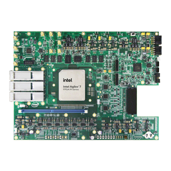
Altera or Intel. Altera and Intel customers are advised to obtain the latest version of device specifications before relying on any published information and before placing orders for products or services. - Page 5 1. Overview 782461 | 2024.05.14 Figure 1. Agilex 7 FPGA M-Series HBM2e Development Kit Top Related Information Agilex 7 FPGA and SoC FPGA M-Series Webpage ™ Agilex 7 FPGA M-Series HBM2e Development Kit User Guide Send Feedback...
-
Page 6: Block Diagram
— Avalon streaming interface x8 configuration mode support — 2 Gb flash for Avalon streaming interface x8 configuration mode — JTAG header for device programming — Built-in Intel FPGA Download Cable II for device programming • Programmable clock sources ™... - Page 7 — 2 X 16 LPDDR5 component, 2 channels and each is 16 bit data line interface • Communication ports — JTAG header — Micro USB on-board Intel FPGA Download Cable II — System I2C header • Buttons, switches, and LEDs —...
-
Page 8: Box Contents
1. Overview 782461 | 2024.05.14 1.3. Box Contents • Agilex 7 FPGA M-Series HBM2e Development Kit • 1x DDR5 DIMM module • 1x IO48 HPS daughter board • USB 2.0 MicroUSB cable • 240W power adapter and NA/EU/JP/UK cords 1.4. Recommended Operating Conditions Table 2. -
Page 9: Getting Started
Altera or Intel. Altera and Intel customers are advised to obtain the latest version of device specifications before relying on any published information and before placing orders for products or services. - Page 10 2. Getting Started 782461 | 2024.05.14 Table 3. Installed Development Kit Directory Structure Directory Name Description of Directory Contents Contains schematics, layout, assembly and bill of material board_design_files board design files. Use these files as a starting point for a new prototype board design Contains the development kit documentation –...
-
Page 11: Development Kit Setup
Altera or Intel. Altera and Intel customers are advised to obtain the latest version of device specifications before relying on any published information and before placing orders for products or services. - Page 12 3. Development Kit Setup 782461 | 2024.05.14 Switch Default Position Notes • ON:ON–disabled • OFF:ON–internal crystal (default) • ON:OFF–CLKIN2 (MCIO) • OFF:OFF–CLKIN3 (SMP) S28[3:4] Set SSC: • ON:X–disabled (default) • OFF:X–AND OUT0 • X:ON–disabled (default) • X:OFF–enable SS on N1 divider OUT6, OUT7 MAX 10 JTAG Enable switch when the JTAG pin sharing is enabled:...
-
Page 13: Powering Up The Development Kit
3. Development Kit Setup 782461 | 2024.05.14 3.2. Powering Up the Development Kit To power up the development kit, follow these steps: 1. Use the provided 300 W power adapter to supply power through J12 and J3. 2. After the power adapter is plugged into J12 and J3, and switch S7 is set to the ON position, DS15 LED illuminates, indicating that the board powered up successfully. -
Page 14: Board Test System
Altera or Intel. Altera and Intel customers are advised to obtain the latest version of device specifications before relying on any published information and before placing orders for products or services. -
Page 15: Setting Up The Bts Gui Running Environment
4. For the Linux system option, download the JavaFX Linux x64 SDK. 4.1.3. Installing OpenJDK and OpenJFX Follow these steps to install the downloaded zip files: 1. On the Windows system, Intel recommends that you unzip the files and put them in the following directory: •... -
Page 16: Installing The Quartus Prime Software
4. Board Test System 782461 | 2024.05.14 4.1.4. Installing the Quartus Prime Software You need to install the Quartus Prime software that can support the silicon on the development kit. The recommended version can be found in the file README.txt under directory. -
Page 17: Testing The Functionality Of The Development Kit
4. Board Test System 782461 | 2024.05.14 You can run BTS GUI with the following scripts: 1. On the Windows system, double-click the files to run BTS, Clock Controller, .bat or Power Monitor GUI. Figure 5. Windows Console 2. On the Linux system, run the shell script with root privilege. Figure 6. -
Page 18: The Bottom Information Bar
The green sign turns gray if the board becomes disconnected. • Intel Quartus Prime Version: Displays the current Quartus Prime version installed and active on your system. The text turns red if your version is older than the required version. Change the environment variable QUARTUS_ROOTDIR if you have installed the right version, but the active version does not meet the requirement. -
Page 19: The Sys Info Tab
4. Board Test System 782461 | 2024.05.14 Follow these steps to configure the FPGA with a test system design: 1. On the Configure menu, click the Configure command that corresponds to the functionality you wish to test. 2. Click Configure in the dialog box that appears to download the corresponding design's SRAM Object File ( ) to the FPGA. -
Page 20: The Gpio Tab
Board Name: Indicates the official name of the board given by the BTS. • Board Revision: Indicates the revision of the board. • MAX Version: Indicates the version of the System Intel MAX 10. JTAG Chain The JTAG chain control shows all the devices currently in the JTAG chain. Note: Both of the systems, MAX 10 and the FPGA must be both in the JTAG chain when you are running the BTS GUI. -
Page 21: The Xcvr Tab
4. Board Test System 782461 | 2024.05.14 The following sections describes the controls on the GPIO tab: User LEDs The User LEDs control displays the current state of the user LEDs. Toggle the LED buttons to turn the board LEDs on and off. Click the All button to reverse the state of all the LEDs. - Page 22 4. Board Test System 782461 | 2024.05.14 The following sections describe controls in the QSFPDD NRZ tab: Status The Status control displays the following status information during the loopback test: • PLL Lock: Shows the PLL locked or unlocked state. •...
- Page 23 4. Board Test System 782461 | 2024.05.14 PMA Setting Allows you to make changes to the PMA parameters that affect the active transceiver interface. The following settings are available for analysis: • Serial Loopback: Displays the signal status between the transmitter and the receiver.
- Page 24 4. Board Test System 782461 | 2024.05.14 Data Type The Data Type control specifies the type of data pattern contained in the transactions. Select the following available data types for analysis: • PRBS7: Pseudo-random 7-bit binary sequences. • PRBS15: Pseudo-random 15-bit binary sequences. •...
- Page 25 4. Board Test System 782461 | 2024.05.14 4.2.5.2. The QSFPDD PAM4 Tab Figure 14. The QSFPDD PAM4 Tab Note: This tab has similar control functions as the QSFPDD NRZ tab. ™ Agilex 7 FPGA M-Series HBM2e Development Kit User Guide Send Feedback...
- Page 26 4. Board Test System 782461 | 2024.05.14 4.2.5.3. The FMC+ NRZ Tab Figure 15. The FMC+ Tab Note: This tab has similar control functions as the QSFPDD NRZ tab. ™ Agilex 7 FPGA M-Series HBM2e Development Kit User Guide Send Feedback...
- Page 27 4. Board Test System 782461 | 2024.05.14 4.2.5.4. The QSFPDD800 PAM4 Tab Figure 16. The QSFPDD800 PAM4 Tab Note: This tab has similar control functions as the QSFPDD NRZ tab. PMA Setting In addition to the PMA settings listed in QSFPDD NRZ —...
-
Page 28: Controlling The On-Board Clock Through Clock Controller Gui
4. Board Test System 782461 | 2024.05.14 Figure 17. QSFPDD800PAM4 Tab — PMA Setting Related Information The QSFPDD NRZ Tab on page 21 4.3. Controlling the On-board Clock through Clock Controller GUI The Clock Controller GUI can control the outputs of on-board Si5391-1/Si5391-2/ Si5392/ Si5395/Si5332/Si5518. -
Page 29: Si5391-1
Sets the programmable oscillator frequency for the selected clock to the value in the output controls for Si5391. Frequency changes might take several milliseconds OUTx to take effect. You might see glitches on the clock during this time. Intel recommends resetting the FPGA logic after changing frequencies. ™... -
Page 30: Si5391-2
4. Board Test System 782461 | 2024.05.14 Import You can generate the register list from the Clockbuilder Pro Software tool and import it into Si5391 to update the settings of the output clocks. Register changes are volatile after power cycling. 4.3.2. -
Page 31: Si5392
4. Board Test System 782461 | 2024.05.14 4.3.3. Si5392 Figure 20. Si5392 Note: This tab has similar control functions as the Si5391-1 tab. ™ Agilex 7 FPGA M-Series HBM2e Development Kit User Guide Send Feedback... -
Page 32: Si5395
4. Board Test System 782461 | 2024.05.14 4.3.4. Si5395 Figure 21. Si5395 Note: This tab has similar control functions as the Si5391-1 tab. ™ Agilex 7 FPGA M-Series HBM2e Development Kit User Guide Send Feedback... -
Page 33: Si5332
4. Board Test System 782461 | 2024.05.14 4.3.5. Si5332 Figure 22. Si5332 Note: This tab has similar control functions as the Si5391-1 tab. There is no default button for this clock but you can use Import or power cycle the board to get default clock frequencies. -
Page 34: Si5518
4. Board Test System 782461 | 2024.05.14 4.3.6. Si5518 Figure 23. Si5518 Import You can generate the register list from the Clockbuilder Pro Software tool and import it into Si5518 to update the settings of RAM. Register changes are volatile after power cycling. -
Page 35: Monitoring On-Board Power Regulator Through Power Monitor Gui
4. Board Test System 782461 | 2024.05.14 Related Information Skyworks Solution More information about the Clockbuilder Pro software. 4.4. Monitoring On-Board Power Regulator through Power Monitor The Power Monitor GUI reports most power rails’ voltage, current, and power information on the board. It also collects temperature from FPGA die, power modules, and diodes assembled on PCB. - Page 36 4. Board Test System 782461 | 2024.05.14 Figure 24. Power Monitor GUI — The Power Tab The following sections describe the details of the Power Monitor GUI. Display Configure • Speed Adjustment: Adjusts the update rate of the current curve. •...
- Page 37 4. Board Test System 782461 | 2024.05.14 Figure 25. Power Monitor GUI—The Temperature Tab Temperature Reads the temperature data from the FPGA die, diodes assembled on the PCB, and the QSFPDD modules. Local Temp Shows the temperature comparison of the local and remote temperature sensors. Beta Comp Enables Beta Compensation for the temperature sensing chips.
-
Page 38: Identifying Test Pass Or Fail-Based On Bts Gui Test Status
4. Board Test System 782461 | 2024.05.14 Related Information Running the BTS GUI on page 16 4.5. Identifying Test Pass or Fail-based on BTS GUI Test Status QSFPDD0/QSFPDD1 Plug QSFPDD0/QSFPDD1 loopback module in J16/J17 before you configure the QSFPDD NRZ/PAM4 example build through the BTS GUI. QSFPDD800 Plug QSFPDD800 loopback module in J18 before you configure the QSFPDD800 PAM4 example build through the BTS GUI. -
Page 39: Development Kit Hardware And Configuration
Altera or Intel. Altera and Intel customers are advised to obtain the latest version of device specifications before relying on any published information and before placing orders for products or services. -
Page 40: Hps Out Of Box Experience (Oobe) Daughter Card
5. Development Kit Hardware and Configuration 782461 | 2024.05.14 5.3.1. HPS Out of Box Experience (OOBE) Daughter Card 1. Plug HPS OOBE daughter card in J9. 2. To test HPS Ethernet capability, connect OOBE’s RJ45 port J3 to the Internet. 3. -
Page 41: Custom Projects For The Development Kit
Altera or Intel. Altera and Intel customers are advised to obtain the latest version of device specifications before relying on any published information and before placing orders for products or services. -
Page 42: Document Revision History For The Agilex 7 Fpga M-Series Hbm2E Development Kit User Guide
Altera or Intel. Altera and Intel customers are advised to obtain the latest version of device specifications before relying on any published information and before placing orders for products or services. -
Page 43: Development Kit Components
Altera or Intel. Altera and Intel customers are advised to obtain the latest version of device specifications before relying on any published information and before placing orders for products or services. -
Page 44: Clocks
A. Development Kit Components 782461 | 2024.05.14 Onboard hot-plug circuit shuts down all power rails when the total power is over 360 W (30 A). UB2/PWR MAX 10 shuts down significant power rails when one or more good power indicators is low due to a power fault. UB2/PWR MAX 10 also shuts down significant power rails when temperature cross the acceptable range. - Page 45 A. Development Kit Components 782461 | 2024.05.14 Schematic Signal Name Default Frequency (MHz) 156.25 CLK_156_25MHZ_SYNCE_DDR_P/N 156.25 CLK_156_25_MHZ_SI5392 CLK_UIB0_P/N CLK_UIB0_FBR0_P/N CLK_UIB0_FBR1_P/N CLK_UIB1_P/N FPGA_IO_CLK0_P/N FPGA_IO_CLK5_P/N CLK_UIB1_FBR0_P/N CLK_UIB1_FBR1_P/N CLK_100M_RP_0_P/N CLK_100M_PCIE1_P/N CLK_100M_PCIE0_P/N CLK_100M_RP_1_P/N CLK_100M_RP_2_P/N CLK_SI5332_U10_IO_PLL_DP CLK_SI5332_U20_IO_PLL_DP CLK_SI5332_U22_IO_PLL_DP CLK_DDR5_RDIMM_A0_DP/DN CLK_DDR5_RDIMM_A1_DP/DN CLK_DDR5_COM_DP/DN CLK_DDR5_COM_HPS_DP/DN CLK_LP5_B1_P/N CLK_LP5_A1_P/N FPGA_IO_CLK_2_P/N CLK_NOC_PLL0 CLK_NOC_PLL1 FPGA_SDM_1V8_125M_CLK...
-
Page 46: General Input/Output
A. Development Kit Components 782461 | 2024.05.14 Figure 27. Clock Tree G.703 10M_I/O 10M, 1.8V Agilex-M SyncE/CPRI Priority FPGA 1.2V CMOS G.703 F-Tile U20 390.625M 1PPSFB DDR5 DIMM0, 100M SLVDS 1PPS OUT 1PPS_I/O 1PPS OUT F-Tile U22 390.625M DDR5 DIMM1, 100M SLVDS F-Tile U20 156.25M 1PPS IN 2x 125M NOC, 1.8V CMOS... - Page 47 A. Development Kit Components 782461 | 2024.05.14 Schematic Signal Name Description QSFPDD PORT 0 LED1 QFPDD_0_3V3_LED1/DS6 QSFPDD PORT 1 LED0 QFPDD_1_3V3_LED0/DS11 QSFPDD PORT 1 LED1 QFPDD_1_3V3_LED1/DS12 QSFPDD800 LED0 QFPDD800_3V3_LED0/DS13 QSFPDD800 LED1 QFPDD800_3V3_LED1/DS14 Reserved MAX10_USER_LED0 F-Tile die, R-Tile die, core die, board overtemp red LED is on OVERTEMP_N/D10,D19 LED is on when MAX 10 configuration is done MAX_CONFIG_DONE/DS10...
-
Page 48: Memory Interfaces
0: On-board Intel FPGA Download Cable II is under reset Fx2_resetn • 1: 0: On-board Intel FPGA Download Cable II is out of reset FPGA Power Good, Agilex 7 M-Series HBM2e power sequences are BOARD_PWR_GOOD_LED/DS15 successful and all the power rails on board are good. - Page 49 A. Development Kit Components 782461 | 2024.05.14 Table 9. MCIO Port Schematic Signal Name Description PCIe endpoint/root port reset PCIE_PERSTn_A PCIe Alert PCIE_ALERTn_A PCIe reference clock PCIE_100M_REF_AP/AN PCIe I C bus PCIE_SCL_A/SDA_A Transceiver TX PCIE_TX_P/N[15:0] Transceiver RX PCIE_RX_P/N[15:0] 2x MCIO x8 Connector The recommended MCIO cable to use with MCIO connector (Uxx) is not included as part of the development kit and must be acquired directly from third party supplier (Amphenol p/n = HMC74-0631).
- Page 50 A. Development Kit Components 782461 | 2024.05.14 Schematic Signal Name Description Mode select QSFPDD1_3V3_MODSEL_L Initial mode QSFPDD1_3V3_LPMODE Interrupt QSFPDD1_3V3_INT_L C clock I2C_QSFPDD1_3V3_SCL C data I2C_QSFPDD1_3V3_SDA Transceiver TX QSFPDD1_TX_P/N[0:7] Transceiver RX QSFPDD1_RX_P/N[0:7] Table 12. QSFPDD800 (J18) Schematic Signal Name Description Module present QSFPDD800_3V3_MODPRS_L Module reset QSFPDD800_3V3_RESET_L...
- Page 51 A. Development Kit Components 782461 | 2024.05.14 Another I C master instance from the system MAX 10 ( ) controls VCXO_I2C_SDA/SCL the on board VCXO and Si5394 clock generator. The Agilex 7 FPGA also manages QSFPDD800, 2x QSFPDD, 1 RDIMM DDR5 I C buses, SDI transceivers, and ZL30733 clock synthesizer device.
-
Page 52: Daughter Card
Voltage Translator MAX31730 MAX31730 TEMP SENSOR TEMP SENSOR HOTSWAP HOTSWAP MAC EEPROM FRUID 0x42H 0x40H 0x5FH 0xA0H 0x1C 0x1DH Intel MAX® 10 MAX10_I2C_1v8_clk_scl/sda SI5392 SI5391 SI5391 SI5391 SI5332 EU122 0x69H 0x75H 0x76H 0x68H 0x6AH fx2_scl/sda USB BLASTER PHY U101 hps_scl/sda... -
Page 53: Connectors And Cables
A. Development Kit Components 782461 | 2024.05.14 • C: HPS I C port • GPIO — 2x Push buttons — 3x LEDs — 1x Ethernet Interrupt from Ethernet PHY — 1x USB over-current indicator • HPS Clock: 25 MHz oscillator A.7. -
Page 54: Additional Information
Altera or Intel. Altera and Intel customers are advised to obtain the latest version of device specifications before relying on any published information and before placing orders for products or services. -
Page 55: Safety Warnings
B. Additional Information 782461 | 2024.05.14 B.1.1. Safety Warnings Power Supply Hazardous Voltage AC mains voltages are present within the power supply assembly. No user serviceable parts are present inside the power supply. Power Connect and Disconnect The AC power supply cord is the primary disconnect device from mains (AC power) and used to remove all DC power from the board/system. -
Page 56: Safety Cautions
B. Additional Information 782461 | 2024.05.14 Power Cord Requirements The plug on the power cord must be a grounding-type male plug designed for use in your region. It must have certification marks showing certification by an agency in your region. The connector that plugs into the appliance inlet of the power supply must be an IEC 320, sheet C13, female connector. - Page 57 B. Additional Information 782461 | 2024.05.14 Cooling Requirements Maintain a minimum clearance area of 5 centimeters (2 inches) around the side, front and back of the board for cooling purposes. Do not block power supply ventilation holes and fan. Electro-Magnetic Interference (EMI) This equipment has not been tested for compliance with emission limits of FCC and similar international regulations.
- Page 58 Failure to use wrist straps can damage components within the system. Attention: Please return this product to Intel for proper disposition. If it is not returned, refer to local environmental regulations for proper recycling. Do not dispose of this product in unsorted municipal waste.
-
Page 59: Compliance Information
B. Additional Information 782461 | 2024.05.14 Please return this product to Intel for proper disposition. If it is not returned, refer to local environmental regulations for proper recycling. Do not dispose of product in unsorted municipal waste. B.2. Compliance Information...
Need help?
Do you have a question about the altera Agilex 7 FPGA M Series and is the answer not in the manual?
Questions and answers