
Related Manuals for Intel Stratix 10 GX FPGA


Summary of Contents for Intel Stratix 10 GX FPGA
- Page 1 ® ® Intel Stratix 10 GX FPGA Development Kit User Guide Subscribe UG-20046 | 2020.04.02 Send Feedback Latest document on the web: HTML Arrow.com. Downloaded from...
-
Page 2: Table Of Contents
Prime Software..............6 2.1.1. Activating Your License................6 2.2. Development Board Package................... 7 2.3. Installing the Intel FPGA Download Cable II Driver............. 8 3. Development Board Setup....................9 3.1. Applying Power to the Development Board..............9 3.2. Default Switch and Jumper Settings............... 10 4. - Page 3 A. Additional Information....................91 A.1. Safety and Regulatory Information.................91 A.1.1. Safety Warnings..................92 A.1.2. Safety Cautions..................93 A.2. Compliance and Conformity Statements..............95 B. Revision History......................96 ® ® Intel Stratix 10 GX FPGA Development Kit User Guide Send Feedback Arrow.com. Arrow.com. Arrow.com. Downloaded from...
-
Page 4: Overview
Intel's standard warranty, but reserves the right to make changes to any products and services Registered at any time without notice. Intel assumes no responsibility or liability arising out of the application or use of any information, product, or service described herein except as expressly agreed to in writing by Intel. Intel customers are advised to obtain the latest version of device specifications before relying on any published information and before placing orders for products or services. -
Page 5: Recommended Operating Conditions
Without proper anti-static handling, the board can be damaged. Therefore, use anti- static handling precautions when touching the board. Caution: This development kit should not be operated in a Vibration environment. ® ® Intel Stratix 10 GX FPGA Development Kit User Guide Send Feedback Arrow.com. Arrow.com. -
Page 6: Getting Started
Intel's standard warranty, but reserves the right to make changes to any products and services Registered at any time without notice. Intel assumes no responsibility or liability arising out of the application or use of any information, product, or service described herein except as expressly agreed to in writing by Intel. Intel customers are advised to obtain the latest version of device specifications before relying on any published information and before placing orders for products or services. -
Page 7: Development Board Package
(DKE) of the Intel Quartus Prime Design Suite software. Your DKE license is valid only for one year and you cannot use this version of the Intel Quartus Prime after one year. To continue using the Intel Quartus Prime software, you should download the free Quartus Prime Lite Edition or purchase a paid license for the Intel Quartus Prime Pro Edition. -
Page 8: Installing The Intel Fpga Download Cable Ii Driver
The development board includes integrated Intel FPGA Download Cable II circuits for FPGA programming. However, for the host computer and board to communicate, you must install the On-Board Intel FPGA Download Cable II driver on the host computer. Installation instructions for the On-Board Intel FPGA Download Cable II driver for your operating system are available on the Intel website. -
Page 9: Development Board Setup
Intel's standard warranty, but reserves the right to make changes to any products and services Registered at any time without notice. Intel assumes no responsibility or liability arising out of the application or use of any information, product, or service described herein except as expressly agreed to in writing by Intel. Intel customers are advised to obtain the latest version of device specifications before relying on any published information and before placing orders for products or services. -
Page 10: Default Switch And Jumper Settings
1.5V FMC select VCCIO R468 1.8V 1.8V FMC select VCCIO Note: A 0 Ohm resistor is installed by default ® ® Intel Stratix 10 GX FPGA Development Kit User Guide Send Feedback Arrow.com. Arrow.com. Arrow.com. Arrow.com. Arrow.com. Arrow.com. Arrow.com. Arrow.com. - Page 11 Switch Board Label Function Default Position Intel Stratix 10 OFF to enable the Intel Stratix 10 in the JTAG chain. ON to bypass the Intel Stratix 10 in the JTAG chain. MAX V OFF to enable the MAX V in the JTAG chain.
- Page 12 I2C_SDA I2C chain Connects VRM I2C to MAX V I2C_SCL I2C chain Connects LT2987 Power FPGA_PWRGD Good to MAX V ® ® Intel Stratix 10 GX FPGA Development Kit User Guide Send Feedback Arrow.com. Arrow.com. Arrow.com. Arrow.com. Arrow.com. Arrow.com. Arrow.com.
-
Page 13: Board Components
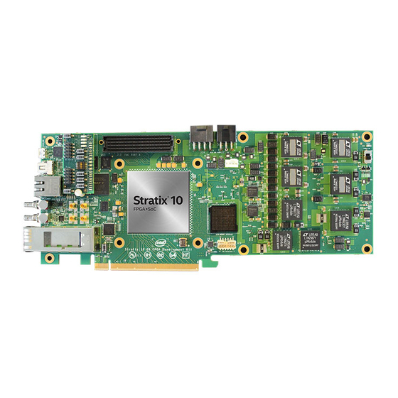
Intel's standard warranty, but reserves the right to make changes to any products and services Registered at any time without notice. Intel assumes no responsibility or liability arising out of the application or use of any information, product, or service described herein except as expressly agreed to in writing by Intel. Intel customers are advised to obtain the latest version of device specifications before relying on any published information and before placing orders for products or services. - Page 14 4. Board Components UG-20046 | 2020.04.02 Figure 5. Intel Stratix 10 GX FPGA Development Board Image - LED Daughter Board Close Up MAX V Reset Button (S3) Program Configuration Push Button (S1) Image Select Button (S2) FPGA User Dip Switch (SW1) General User Push Buttons (S5, S6, S7) Refer to “Table: Board Specific...
- Page 15 Enables PCI Express link widths x1, x4, x8 and x16. JTAG Bypass DIP Switch Enables and disables devices in the JTAG chain. This switch is located on the back of the board. Configuration DIP Switch Sets the Intel Stratix 10 pins. MSEL MSEL Board settings DIP Switch...
- Page 16 QSFP connector Four TX/RX channels from FPGA Bank 1K J17, J18 SDI HDBNC Video Connector Single TX/RX channel from FPGA bank 1N. continued... ® ® Intel Stratix 10 GX FPGA Development Kit User Guide Send Feedback Arrow.com. Arrow.com. Arrow.com. Arrow.com.
- Page 17 Gbps Ethernet RJ-45 connector RJ-45 connector which provides a 10/100/1000 Ethernet connection via a Marvell 88E1111 PHY and the FPGA-based Intel Triple Speed Ethernet MAC Intel FPGA IP core function in SGMII mode. QSFP Interface Provides four transceiver channels for a 40G/100G QSFP module.
-
Page 18: Max V Cpld System Controller
4. Board Components UG-20046 | 2020.04.02 4.2. MAX V CPLD System Controller The development board utilizes the EPM2210 System Controller, an Intel MAX V CPLD for the following purposes: • FPGA configuration from flash memory • Power consumption monitoring •... - Page 19 4. Board Components UG-20046 | 2020.04.02 Schematic Signal Name Pin Number I/O Standard Description 1.8V MAX V to Intel MAX 10 Intel USB_CFG1 FPGA Download Cable bus 1.8V MAX V to Intel MAX 10 Intel USB_CFG13 FPGA Download Cable bus 1.8V...
- Page 20 FLASH_DATA0 1.8V Flash data bus FLASH_DATA1 1.8V Flash data bus FLASH_DATA2 1.8V Flash data bus FLASH_DATA3 continued... ® ® Intel Stratix 10 GX FPGA Development Kit User Guide Send Feedback Arrow.com. Arrow.com. Arrow.com. Arrow.com. Arrow.com. Arrow.com. Arrow.com. Arrow.com. Arrow.com. Arrow.com.
- Page 21 1.8V FPGA configuration data bus FPGA_CONFIG_D8 1.8V FPGA configuration data bus FPGA_CONFIG_D9 1.8V FPGA configuration data bus FPGA_CONFIG_D10 continued... ® ® Intel Stratix 10 GX FPGA Development Kit User Guide Send Feedback Arrow.com. Arrow.com. Arrow.com. Arrow.com. Arrow.com. Arrow.com. Arrow.com. Arrow.com.
- Page 22 SDI device MF0 SDI_MF0_BYPASS 1.8V SDI device MF1 SDI_MF1_AUTO_SLEEP 1.8V SDI device SD/HD SDI_TX_SD_HDn 1.8V nCONFIG configuration FPGA_nCONFIG signal ® ® Intel Stratix 10 GX FPGA Development Kit User Guide Send Feedback Arrow.com. Arrow.com. Arrow.com. Arrow.com. Arrow.com. Arrow.com. Arrow.com. Arrow.com. Arrow.com. Arrow.com.
-
Page 23: Fpga Configuration
You can use the Quartus Programmer to configure the FPGA with your SRAM Object File (.sof). Ensure the following: • The Quartus Programmer and the Intel FPGA Download Cable II driver are installed on the host computer. • The micro-USB cable is connected to the FPGA development board. - Page 24 LED Daughter Board External JTAG S10_JTAG Intel Stratix 10 FPGA (U1) MAX 10 M5_JTAG MAX V System Intel FPGA Download Cable II Controller (U11) (U23) FMCA_JTAG FMCA (J13) Dedicated USB MAX 10 JTAG USB JTAG Header from LED Daughter Board ®...
-
Page 25: Status Elements
4. Board Components UG-20046 | 2020.04.02 4.4. Status Elements The Intel Stratix 10 GX FPGA development board includes status LEDs as listed below. Table 12. Board-Specific Status LEDs Board Reference Schematic Signal Name I/O Standard D3 on the LED board 2.5V... -
Page 26: User Input-Output Components
MAX_RESETn 4.5.2. User-Defined DIP Switches The Intel Stratix 10 GX FPGA development board includes a set of four pin DIP switch. There are no board-specific functions for these switches. When the switch is in the OFF position, logic 1 is selected. When the switch is in the ON position, logic 0 is selected. - Page 27 USER_LED_R0 D7 on LED board 1.8V USER_LED_R1 D9 on LED board 1.8V USER_LED_R2 D10 on LED board 1.8V USER_LED_R3 ® ® Intel Stratix 10 GX FPGA Development Kit User Guide Send Feedback Arrow.com. Arrow.com. Arrow.com. Arrow.com. Arrow.com. Arrow.com. Arrow.com. Arrow.com.
-
Page 28: Components And Interfaces
The PCI Express interface supports auto-negotiating channel width from x1 to x4 to x8 to x16 by using Intel's PCIe Intel FPGA IP. You can also configure this board to a x1, x4, x8 or x16 interface through a DIP switch that connects the... - Page 29 Receive bus PCIE_RX_P7 AW43 1.4 V PCML Receive bus PCIE_RX_P8 AY45 1.4 V PCML Receive bus PCIE_RX_P9 continued... ® ® Intel Stratix 10 GX FPGA Development Kit User Guide Send Feedback Arrow.com. Arrow.com. Arrow.com. Arrow.com. Arrow.com. Arrow.com. Arrow.com. Arrow.com. Arrow.com.
-
Page 30: 10/100/1000 Ethernet Phy
FPGA IP core MAC function. The PHY-to-MAC interface employs SGMII using the Intel Stratix 10 GX FPGA LVDS pins in Soft-CDR mode at 1.25 Gbps transmit and receive. In 10 Mb or 100 Mb mode, the SGMII interface still runs at 1.25 GHz but the packet data is repeated 10 or 100 times. -
Page 31: Hilo External Memory Interface
MDI_P3 interface 4.6.3. HiLo External Memory Interface This section describes the Intel Stratix 10 GX FPGA development board's external memory interface support and also their signal names, types and connectivity relative to the Intel Stratix 10 GX FPGA. The HiLo connector supports plugins for the following memory interfaces: •... - Page 32 MEM_ADDR_CMD29 Adjustable MEM_ADDR_CMD30 Adjustable MEM_ADDR_CMD31 Adjustable MEM_CLK_N Adjustable MEM_CLK_P Adjustable MEM_DMA0 Adjustable MEM_DMA1 continued... ® ® Intel Stratix 10 GX FPGA Development Kit User Guide Send Feedback Arrow.com. Arrow.com. Arrow.com. Arrow.com. Arrow.com. Arrow.com. Arrow.com. Arrow.com. Arrow.com. Arrow.com. Arrow.com. Arrow.com. Arrow.com.
- Page 33 MEM_DQA12 Adjustable MEM_DQA13 Adjustable MEM_DQA14 Adjustable MEM_DQA15 Adjustable MEM_DQA16 Adjustable MEM_DQA17 Adjustable MEM_DQA18 continued... ® ® Intel Stratix 10 GX FPGA Development Kit User Guide Send Feedback Arrow.com. Arrow.com. Arrow.com. Arrow.com. Arrow.com. Arrow.com. Arrow.com. Arrow.com. Arrow.com. Arrow.com. Arrow.com. Arrow.com. Arrow.com.
- Page 34 MEM_DQB12 Adjustable MEM_DQB13 Adjustable MEM_DQB14 Adjustable MEM_DQB15 Adjustable MEM_DQB16 Adjustable MEM_DQB17 Adjustable MEM_DQB18 continued... ® ® Intel Stratix 10 GX FPGA Development Kit User Guide Send Feedback Arrow.com. Arrow.com. Arrow.com. Arrow.com. Arrow.com. Arrow.com. Arrow.com. Arrow.com. Arrow.com. Arrow.com. Arrow.com. Arrow.com. Arrow.com.
- Page 35 MEM_DQSB_N2 Adjustable MEM_DQSB_N3 Adjustable MEM_DQSB_P0 Adjustable MEM_DQSB_P1 Adjustable MEM_DQSB_P2 Adjustable MEM_DQSB_P3 Adjustable MEM_QKA_P0 continued... ® ® Intel Stratix 10 GX FPGA Development Kit User Guide Send Feedback Arrow.com. Arrow.com. Arrow.com. Arrow.com. Arrow.com. Arrow.com. Arrow.com. Arrow.com. Arrow.com. Arrow.com. Arrow.com. Arrow.com. Arrow.com.
-
Page 36: Fmc
Adjustable MEM_QKB_P1 4.6.4. FMC The Intel Stratix 10 GX FPGA development board includes a high pin count (HPC) FPGA mezzanine card (FMC) connector that functions with a quadrature amplitude modulation (QAM) digital-to-analog converter (DAC) FMC module or daughtercard. This pin-out satisfies a QAM DAC that requires 58 low-voltage differential signaling (LVDS) data output pairs, one LVDS input clock pair and three low-voltage LVDS control pairs from the FPGA device. - Page 37 FMCA_DP_M2C_N12 1.4V PCML FMCA_DP_M2C_N13 1.4V PCML FMCA_DP_M2C_N14 1.4V PCML FMCA_DP_M2C_N15 1.4V PCML FMCA_DP_M2C_P0 1.4V PCML FMCA_DP_M2C_P1 continued... ® ® Intel Stratix 10 GX FPGA Development Kit User Guide Send Feedback Arrow.com. Arrow.com. Arrow.com. Arrow.com. Arrow.com. Arrow.com. Arrow.com. Arrow.com. Arrow.com. Arrow.com.
- Page 38 FMCA_LA_RX_N0 AR21 LVDS FMCA_LA_RX_N1 AR18 LVDS FMCA_LA_RX_N2 AP20 LVDS FMCA_LA_RX_N3 AP16 LVDS FMCA_LA_RX_N4 continued... ® ® Intel Stratix 10 GX FPGA Development Kit User Guide Send Feedback Arrow.com. Arrow.com. Arrow.com. Arrow.com. Arrow.com. Arrow.com. Arrow.com. Arrow.com. Arrow.com. Arrow.com. Arrow.com. Arrow.com. Arrow.com.
- Page 39 FMCA_LA_TX_N4 AW11 LVDS FMCA_LA_TX_N5 BB18 LVDS FMCA_LA_TX_N6 AY12 LVDS FMCA_LA_TX_N7 BD18 LVDS FMCA_LA_TX_N8 continued... ® ® Intel Stratix 10 GX FPGA Development Kit User Guide Send Feedback Arrow.com. Arrow.com. Arrow.com. Arrow.com. Arrow.com. Arrow.com. Arrow.com. Arrow.com. Arrow.com. Arrow.com. Arrow.com. Arrow.com. Arrow.com.
- Page 40 3.3V FMCA_SDA – – VIO_B_M2C – – VIO_B_M2C – – VREF_B_M2C – – VREF_FMC ® ® Intel Stratix 10 GX FPGA Development Kit User Guide Send Feedback Arrow.com. Arrow.com. Arrow.com. Arrow.com. Arrow.com. Arrow.com. Arrow.com. Arrow.com. Arrow.com. Arrow.com. Arrow.com. Arrow.com. Arrow.com.
-
Page 41: Qsfp
4. Board Components UG-20046 | 2020.04.02 4.6.5. QSFP The Intel Stratix 10 GX FPGA development board includes a Quad Small Form-Factor Pluggable (QSFP) module. Table 20. QSFP Pin Assignments Board Reference Schematic Signal FPGA Pin Number I/O Standard Description Name BE26 1.8V... -
Page 42: I 2 C
VID regulators, ADC and temperature sensors. You can use the Intel Stratix 10 or MAX V as the I C host to access these devices, change clock frequencies or get board status information such as voltage and temperature readings. -
Page 43: Displayport
BH20 1.8V Dedicated I C to FMC FMCA_SDA Connector 4.6.7. DisplayPort The Intel Stratix 10 GX FPGA development board includes a Mini-DisplayPort connector. Table 26. Mini-DisplayPort Schematic Signal Names and Functions Board Reference Schematic Signal FPGA Pin Number I/O Standard... -
Page 44: Sdi Video Input/Output Ports
DP_ML_LANE_CP3 4.6.8. SDI Video Input/Output Ports The Intel Stratix 10 GX FPGA development board includes a SDI port, which consists of a M23428G-33 cable driver and a M23544G-14 cable equalizer. The PHY devices from Macom interface to single-ended HDBNC connectors. - Page 45 – – SDI_EQIN_N1 U21.3 – – SDI_EQIN_P1 U21.14 1.4V PCML SDO_N/SDI_RX_N U21.15 1.4V PCML SDO_P/SDI_RX_P ® ® Intel Stratix 10 GX FPGA Development Kit User Guide Send Feedback Arrow.com. Arrow.com. Arrow.com. Arrow.com. Arrow.com. Arrow.com. Arrow.com. Arrow.com. Arrow.com. Arrow.com. Arrow.com. Arrow.com.
-
Page 46: Clock Circuits
4. Board Components UG-20046 | 2020.04.02 4.7. Clock Circuits 4.7.1. On-Board Oscillators Figure 11. Intel Stratix 10 GX FPGA Board - Clock Inputs and Default Frequencies REFCLK1 (155.52 MHz LVDS) OUT0 REFCLK_QSFPI1 (644.53125 MHz LVDS) OUT1 REFCLK_DP (135 MHz LVDS) -
Page 47: Off-Board Clock I/O
The output clocks can be programmed to different levels and I/O standards according to the FPGA device's specification. Table 32. Off-Board Clock Inputs Source Schematic Signal I/O Standard Intel Stratix 10 FPGA Description Name Pin Number LVDS SDI Refclk Input SDI_REFCLK_SMA_P... -
Page 48: Memory
FPGA. 4.8.1. Flash The Intel Stratix 10 GX FPGA development board supports two 1 GB CFI-compatible synchronous flash devices for non-volatile storage of FPGA configuration data, board information, test application data and user code space. These devices are part of the shared bus that connects to the flash memory, FPGA and MAX V CPLD EPM2210 System Controller. - Page 49 BE36 1.8V Data bus FLASH_DATA1 BC35 1.8V Data bus FLASH_DATA2 BC36 1.8V Data bus FLASH_DATA3 continued... ® ® Intel Stratix 10 GX FPGA Development Kit User Guide Send Feedback Arrow.com. Arrow.com. Arrow.com. Arrow.com. Arrow.com. Arrow.com. Arrow.com. Arrow.com. Arrow.com. Arrow.com. Arrow.com.
-
Page 50: Programming Flash Using Quartus Programmer
Object File (.pof). Ensure the following conditions are met before you proceed: • The Quartus Programmer and the Intel FPGA Download Cable II driver are installed on the host computer. • The micro-USB cable is connected to the FPGA development board. - Page 51 Board Test System and the Power Monitor to lose their connection to the board. Restart those applications after programming is complete. ® ® Intel Stratix 10 GX FPGA Development Kit User Guide Send Feedback Arrow.com.
-
Page 52: Daughtercards
4. Board Components UG-20046 | 2020.04.02 4.9. Daughtercards The Intel Stratix 10 GX FPGA development kit provides a full-featured hardware development platform for prototyping and testing high-speed interfaces to a Intel Stratix 10 GX FPGA. Table 37. Intel Stratix 10 FPGA Development Kit Daughtercards... - Page 53 The RLDRAM3 x36 (reduced latency DRAM) controller is designed for use in applications requiring high memory throughput, high clock rates and full programmability. Figure 14. RLDRAM3 Block Diagram ® ® Intel Stratix 10 GX FPGA Development Kit User Guide Send Feedback Arrow.com. Arrow.com. Arrow.com.
- Page 54 4.9.1.5. FMC Loopback Card The Intel Stratix 10 GX FPGA development kit provides one FMC mezzanine interface port connected to the Intel Stratix 10 GX FPGA for interfacing to the Intel FMC add-in boards as shown in the figure below.
- Page 55 Intel Stratix 10 GX FPGA Development Kit FMC Block Diagram FMCA Port FMCA Intel Stratix 10 GX FPGA The following table shows the complete signal connections assigned for Intel FMC interface at the FMCA port. Table 38. FMCA Connector (J13) Signal Assignments Number...
- Page 56 A_TX_P A_RX_N P_C2M_ FMCA_D FMCA_L FMCA_L FMCA_L FMCA_D P_C2M_ A_TX_N A_TX_P A_RX_P P_C2M_ continued... ® ® Intel Stratix 10 GX FPGA Development Kit User Guide Send Feedback Arrow.com. Arrow.com. Arrow.com. Arrow.com. Arrow.com. Arrow.com. Arrow.com. Arrow.com. Arrow.com. Arrow.com. Arrow.com. Arrow.com. Arrow.com.
- Page 57 A10_VC A10_VC 3.3V CIO_FM CIO_FM A10_VC A10_VC 3.3V CIO_FM CIO_FM Connect Connect Connect Connect ® ® Intel Stratix 10 GX FPGA Development Kit User Guide Send Feedback Arrow.com. Arrow.com. Arrow.com. Arrow.com. Arrow.com. Arrow.com. Arrow.com. Arrow.com. Arrow.com. Arrow.com. Arrow.com. Arrow.com. Arrow.com.
- Page 58 The Low Pin Count FMC connections are assigned to columns C and D in the FMCA connector as shown. The LPC signaling follows the Vita57.1 standard. ® ® Intel Stratix 10 GX FPGA Development Kit User Guide Send Feedback Arrow.com.
-
Page 59: System Power
Intel's standard warranty, but reserves the right to make changes to any products and services Registered at any time without notice. Intel assumes no responsibility or liability arising out of the application or use of any information, product, or service described herein except as expressly agreed to in writing by Intel. Intel customers are advised to obtain the latest version of device specifications before relying on any published information and before placing orders for products or services. -
Page 60: Power Distribution System
PCIe slot or the 2x4 power connector (J26). The power switch SW7 controls powering the board on/off. 5.2. Power Distribution System The following figure below shows the power distribution system on the Intel Stratix 10 GX FPGA development board. ® ®... -
Page 61: Power Measurement
C bus connects the ADC device to the MAX V CPLD EPM2210 System Controller as well as the Intel Stratix 10 GX FPGA. The VCC rail for the FPGA core power is directly measured by the LTM4677 I enabled voltage regulator module. Power measurements can be read from the... -
Page 62: Thermal Limitations And Protection
UG-20046 | 2020.04.02 5.4. Thermal Limitations and Protection The Intel Stratix 10 GX FPGA development kit is designed to operate in a typical laboratory environment with an ambient temperature of approximately 25C. The cooling solution provided with the development kit allows sufficient cooling for the board to operate up to a maximum power consumption of 200 W under this environment. -
Page 63: Board Test System
Intel's standard warranty, but reserves the right to make changes to any products and services Registered at any time without notice. Intel assumes no responsibility or liability arising out of the application or use of any information, product, or service described herein except as expressly agreed to in writing by Intel. Intel customers are advised to obtain the latest version of device specifications before relying on any published information and before placing orders for products or services. -
Page 64: Preparing The Board
BTS and Power Monitor share the JTAG bus with other applications like the Nios II debugger and the Signal Tap II Embedded Logic Analyzer. Because the BTS is designed based on the Intel Quartus Prime software, be sure to close other applications before you use the BTS. -
Page 65: Running The Board Test System
Use the Configure Menu to select the design you want to use. Each design example tests different board features. Select a design from this menu and the corresponding tabs become active for testing. ® ® Intel Stratix 10 GX FPGA Development Kit User Guide Send Feedback Arrow.com. -
Page 66: The System Info Tab
FPGA. The corresponding GUI application tabs that interface with the design are now enabled. If you use the Intel Quartus Prime Programmer for configuration, rather than the BTS GUI, you may need to restart the GUI. - Page 67 Newer <package dir>\examples\max5 revisions of this code may be available on the Intel Stratix 10 GX FPGA Development kit link on the Intel website. The MAX V register control allows you to view and change the current MAX V register values as described in the table below.
-
Page 68: The Gpio Tab
You can read DIP switch settings, turn LEDs on or off and detect push button presses. Figure 22. The GPIO Tab ® ® Intel Stratix 10 GX FPGA Development Kit User Guide Send Feedback Arrow.com. Arrow.com. Arrow.com. -
Page 69: The Flash Tab
The Flash tab allows you to read and write flash memory on your board. The memory table displays the CFI ROM contents by default after you configure the FPGA. ® ® Intel Stratix 10 GX FPGA Development Kit User Guide Send Feedback Arrow.com. - Page 70 Starts a random data pattern test to flash memory, limited to the 512K test system scratch page. Updates the memory table, displaying the CFI ROM table contents from the flash device. ® ® Intel Stratix 10 GX FPGA Development Kit User Guide Send Feedback Arrow.com. Arrow.com.
-
Page 71: The Xcvr Tab
This tab allows you to perform loopback tests on the QSFP and SDI ports. Figure 24. The XCVR Tab Status Displays the following status information during a loopback test: ® ® Intel Stratix 10 GX FPGA Development Kit User Guide Send Feedback Arrow.com. Arrow.com. Arrow.com. - Page 72 • DC gain: Specifies the DC gain setting for the receiver equalizer in four stage mode. • VGA: Specifies the VGA gain value. ® ® Intel Stratix 10 GX FPGA Development Kit User Guide Send Feedback Arrow.com. Arrow.com. Arrow.com. Arrow.com.
- Page 73 Stop: Terminates transaction performance analysis. • TX and RX performance bars: Show the percentage of maximum theoretical data rate that the requested transactions are able to achieve. ® ® Intel Stratix 10 GX FPGA Development Kit User Guide Send Feedback Arrow.com. Arrow.com.
-
Page 74: The Pcie Tab
Figure 25. The PCIe Tab The following sections describe the controls on the PCIe tab. Status Displays the following status information during a loopback test: ® ® Intel Stratix 10 GX FPGA Development Kit User Guide Send Feedback Arrow.com. Arrow.com. Arrow.com. - Page 75 PCIe x16 Gen3 PMA Setting Allows you to make changes to the PMA parameters that affect the active transceiver interface. The following settings are available for analysis: ® ® Intel Stratix 10 GX FPGA Development Kit User Guide Send Feedback Arrow.com. Arrow.com.
- Page 76 VGA: Specifies the VGA gain value. • All PMA settings should be changed as given in the figure below: Figure 26. PMA Settings ® ® Intel Stratix 10 GX FPGA Development Kit User Guide Send Feedback Arrow.com. Arrow.com. Arrow.com. Arrow.com.
-
Page 77: The Fmc Tab
6.3.7. The FMC Tab This tab allows you to perform loopback tests on the FMC port. ® ® Intel Stratix 10 GX FPGA Development Kit User Guide Send Feedback Arrow.com. Arrow.com. - Page 78 Figure 27. The FMC Tab The following sections describe controls in the FMC tab. Status Displays the following status information during a loopback test: ® ® Intel Stratix 10 GX FPGA Development Kit User Guide Send Feedback Arrow.com. Arrow.com. Arrow.com.
- Page 79 CMOS PMA Settings Allows you to make changes to the PMA parameters that affect the active transceiver interface. The following settings are available for analysis: ® ® Intel Stratix 10 GX FPGA Development Kit User Guide Send Feedback Arrow.com. Arrow.com.
- Page 80 DC gain: Specifies the DC gain setting for the receiver equalizer in four stage mode. • VGA: Specifies the VGA gain value. Figure 28. PMA Settings ® ® Intel Stratix 10 GX FPGA Development Kit User Guide Send Feedback Arrow.com. Arrow.com. Arrow.com. Arrow.com.
-
Page 81: The Ddr3 Tab
6.3.8. The DDR3 Tab This tab allows you to read and write DDR3 memory on your board. ® ® Intel Stratix 10 GX FPGA Development Kit User Guide Send Feedback Arrow.com. - Page 82 2133 Mbps per pin. Equating to a theoretical maximum bandwidth of 136512 Mbps or 17064 MBps. Error Control This control displays data errors detected during analysis and allows you to insert errors: ® ® Intel Stratix 10 GX FPGA Development Kit User Guide Send Feedback Arrow.com. Arrow.com. Arrow.com.
-
Page 83: The Ddr4 Tab
The DDR4 Tab The following sections describe the controls on the DDR4 tab. Start Initiates DDR4 memory transaction performance analysis. Stop Terminates transaction performance analysis. ® ® Intel Stratix 10 GX FPGA Development Kit User Guide Send Feedback Arrow.com. Arrow.com. Arrow.com. Arrow.com. -
Page 84: Power Monitor
<package dir>\examples\board_test_system Note: You cannot run the stand-alone power application and the BTS simultaneously. Also, you cannot run power and clock interface at the same time. ® ® Intel Stratix 10 GX FPGA Development Kit User Guide Send Feedback Arrow.com. Arrow.com. - Page 85 The red line indicates the maximum value read since the last reset. The yellow line indicates the minimum value read since the last reset. ® ® Intel Stratix 10 GX FPGA Development Kit User Guide Send Feedback Arrow.com.
-
Page 86: Clock Controller
The Clock Control communicates with the MAX V on the board through the JTAG bus. The programmable oscillator are connected to the MAX V device through a 2-wire serial bus. Figure 32. Clock Controller - Si5338 ® ® Intel Stratix 10 GX FPGA Development Kit User Guide Send Feedback Arrow.com. Arrow.com. Arrow.com. - Page 87 Display the current frequencies for each oscillator. Frequency Allows you to specify the frequency of the clock MHz. Set enable or disable Spread Spectrum Clocking. ® ® Intel Stratix 10 GX FPGA Development Kit User Guide Send Feedback Arrow.com. Arrow.com.
-
Page 88: Smart Vid Setting
Sets the programmable oscillator frequency for the selected clock to the value in the CLK0 to CLK3 controls for the Si5338. Frequency changes might take several milliseconds to take effect. You might see glitches on the clock during this time. Intel recommends resetting the FPGA logic after changing frequencies. - Page 89 6. Board Test System UG-20046 | 2020.04.02 Figure 34. Power Management & VID ® ® Intel Stratix 10 GX FPGA Development Kit User Guide Send Feedback Arrow.com. Arrow.com. Arrow.com. Arrow.com. Arrow.com. Arrow.com. Arrow.com. Arrow.com. Arrow.com. Arrow.com. Arrow.com. Arrow.com. Arrow.com. Arrow.com.
- Page 90 6. Board Test System UG-20046 | 2020.04.02 Figure 35. Configuration PIN ® ® Intel Stratix 10 GX FPGA Development Kit User Guide Send Feedback Arrow.com. Arrow.com. Arrow.com. Arrow.com. Arrow.com. Arrow.com. Arrow.com. Arrow.com. Arrow.com. Arrow.com. Arrow.com. Arrow.com. Arrow.com. Arrow.com. Arrow.com. Arrow.com.
-
Page 91: Additional Information
Intel's standard warranty, but reserves the right to make changes to any products and services Registered at any time without notice. Intel assumes no responsibility or liability arising out of the application or use of any information, product, or service described herein except as expressly agreed to in writing by Intel. Intel customers are advised to obtain the latest version of device specifications before relying on any published information and before placing orders for products or services. -
Page 92: Safety Warnings
To avoid shock, you must ensure that the power cord is connected to a properly wired and grounded receptacle. Ensure that any equipment that attaches to this product is also connected to properly wired and grounded receptacles. ® ® Intel Stratix 10 GX FPGA Development Kit User Guide Send Feedback Arrow.com. -
Page 93: Safety Cautions
Certain components such as heat sinks, power regulators, and processors may be hot. Heatsink fans are not guarded. Power supply fan may be accessible through guard. Care should be taken to avoid contact with these components. ® ® Intel Stratix 10 GX FPGA Development Kit User Guide Send Feedback Arrow.com. - Page 94 Public Switched Telecommunication Network (PSTN) as it might result in disruption of the network. No formal telecommunication certification to FCC, R&TTE Directive, or other national requirements have been obtained. ® ® Intel Stratix 10 GX FPGA Development Kit User Guide Send Feedback Arrow.com.
-
Page 95: Compliance And Conformity Statements
Failure to use wrist straps can damage components within the system. Attention: Please return this product to Intel for proper disposition. If it is not returned, refer to local environmental regulations for proper recycling. Do not dispose of this product in unsorted municipal waste. -
Page 96: Revision History
Intel's standard warranty, but reserves the right to make changes to any products and services Registered at any time without notice. Intel assumes no responsibility or liability arising out of the application or use of any information, product, or service described herein except as expressly agreed to in writing by Intel. Intel customers are advised to obtain the latest version of device specifications before relying on any published information and before placing orders for products or services.
Need help?
Do you have a question about the Stratix 10 GX FPGA and is the answer not in the manual?
Questions and answers