Table of Contents
Advertisement
Quick Links
Advertisement
Chapters
Table of Contents

Subscribe to Our Youtube Channel
Related Manuals for Fuji Electric micrex-sx SPH


Summary of Contents for Fuji Electric micrex-sx SPH
- Page 1 series USER'S MANUAL PULSE TRAIN POSITIONING CONTROL COMBINED MODULE FEH214a...
- Page 2 Preface This User’s Manual explains the pulse train positioning control combined module. Read this manual carefully to ensure correct operation. When using modules or peripheral devices, be sure to read the corresponding user’s manuals listed below. s ' r s ' r c i f s ' r I <...
- Page 3 Safety Precautions Be sure to read the “Safety Precautions” thoroughly before using the module. Here, the safety precaution items are classified into “Warning” and “Caution.” Warning Incorrect handling of the device may result in death or serious injury. Caution Incorrect handling of the device may result in minor injury or physical damage. Even some items indicated by “Caution”...
- Page 4 ◊ Do not attemp to repair the module by yourself contact your Fuji Electric agent. When replacing the batteries, correctly and securely connect the battery connectors, otherwise, fire, accidents or failure might occure.
- Page 5 Revision...
-
Page 6: Table Of Contents
Contents Preface Safety Precautions Revision Contents page Section 1 General ..................1-1 1-1 Precautions ............................. 1-1 1-2 Functional Overview ........................1-2 1-2-1 Overview of NP1F-MP1/NP1F-MP2 functions ..................1-2 1-2-2 Overview of NP2F-LEV functions ......................1-3 Section 2 System Configuration ..............2-1 2-1 Configuration of Peripheral Equipment .................. - Page 7 Contents page 4-5 Connecting ............................. 4-21 4-5-1 Connecting sample of a servo motor ....................4-21 4-6 I/O Wiring ............................4-24 Section 5 Memory Map .................5-1 5-1 NP1F-MP1/NP1F-MP2 Memory Map (Internal Memory List) ............5-1 5-2 NP1F-MP1 I/O Area ......................... 5-2 5-2-1 NP1F-MP1 (read area: address No.
- Page 8 Contents page 7-4 Functions of the Position Command Mode ................7-31 7-4-1 Positional deviation calculation ......................7-32 7-4-2 Operation at the rising edge of start signal ..................7-33 7-4-3 Operation when start command is “ON” ....................7-33 7-4-4 Processing when start command is turned OFF ................. 7-35 7-4-5 Original point return motion .........................
-
Page 9: Section 1 General
Section 1 General Page 1-1 Precautions ......................... 1-1 (1) Handling precautions as precision device ....................1-1 (2) Precautions concerning operating conditions and environment ............. 1-1 1-2 Functional Overview ....................1-2 1-2-1 Overview of NP1F-MP1/NP1F-MP2 functions ..............1-2 1-2-2 Overview of NP2F-LEV functions ..................1-3... -
Page 10: Precautions
(performance), take sufficient fail-safe measures, and be sure to consult with personnel at your Fuji Electric sales office. 1) Storage or use in conditions or an environment which is not described in the operating instructions or user's... -
Page 11: Functional Overview
1-2 Functional Overview 1-2-1 Overview of NP1F-MP1/NP1F-MP2 functions e l l c i t c i t l a i A sample connection configuration of the NP1F-MP1 is shown below: Sample connection configuration of the NP1F-MP1 NP1F-MP1 X-axis forward/reverse pulse Servo Motor Serial... -
Page 12: Overview Of Np2F-Lev Functions
1-2 Functional Overview 1-2-2 Overview of NP2F-LEV functions e l l n i l A sample connection configuration of the NP2F-LEV is shown below: Sample connection configuration of the NP2F-LEV NP1F-MP2 NP2F-LEV X-axis Serial forward pulse Motor Servo X-axis amplifier reverse pulse Encoder Y-axis... - Page 13 1-2 Functional Overview A sample connection configuration of the NP2F-LEV and NP1F-MP1 is as follows: Sample connection configuration of the NP2F-LEV NP2F-LEV NP1F-MP1 Serial X-axis forward pulse Motor Servo SX bus X-axis amplifier reverse pulse Encoder NP2F-LEV Feedback pulse Phase-A External I/Fs Phase-B Phase-Z...
-
Page 14: Section 2 System Configuration
Section 2 System Configuration Page 2-1 Configuration of Peripheral Equipment ..............2-1 2-2 Applied System ......................2-2 2-2-1 Applicable CPU ........................2-2 2-2-2 Applied system configuration ....................2-2 (1) For a 2-axis system ..........................2-2 (2) Sample extensions (for 8-axis system) ....................2-2 2-3 Loader and Software Modules to be Used ............... -
Page 15: Configuration Of Peripheral Equipment
Section 2 System Configuration 2-1 Configuration of Peripheral Equipment The overall configuration of the MICREX-SX series CPU and peripheral equipment is shown below: Overall configuration Positioning CPU module control module NP1PS- NP1F-MP1 NP1F-MP2 Signal converter SX bus Servo NP2F-LEV Motor amplifier (Various-type expansion... -
Page 16: Applied System
2-2 Applied System 2-2-1 Applicable CPU The NP1F-MP1/NP1F-MP2 can be used with a MICREX-SX series CPU. 1) High-performance CPU module ..NP1PS- 2) Standard CPU module ..NP1PH- 2-2-2 Applied system configuration The NP1F-MP1/NP1F-MP2 is connected to the CPU module via an SX bus. Sample connections are shown below: (1) For a 2-axis system Output module... -
Page 17: Loader And Software Modules To Be Used
2-3 Loader and Software Modules to be Used As shown in the above overall configuration, the following loader and software modules are necessary to operate the NP1F-MP1/NP1F-MP2. t i r c i l c i l t i s · e l l l a i ·... -
Page 18: Section 3 Specifications
Section 3 Specifications Page 3-1 General Specifications (NP1F-MP1/NP1F-MP2) ............3-1 3-1-1 General specifications (NP2F-LEV) ..................3-2 3-2 Specifications (NP1F-MP1/NP1F-MP2) ..............3-3 3-2-1 Specifications (NP2F-LEV) ....................3-3 3-3 Names .......................... 3-4 3-3-1 NP1F-MP1 (for 1 axis) ......................3-4 3-3-2 NP1F-MP2 (for 2 axes) ......................3-6 3-3-3 NP2F-LEV (Signal converter) .................... -
Page 19: General Specifications (Np1F-Mp1/Np1F-Mp2)
Section 3 Specifications 3-1 General Specifications (NP1F-MP1/NP1F-MP2) Ω ° C ° C v i t y t i v i t l l o l i o y t i i t l i t l i l p y l l y l l µ... -
Page 20: General Specifications (Np2F-Lev)
3-1 General Specifications (NP1F-MP1/NP1F-MP2) 3-1-1 General specifications (NP2F-LEV) , ) l ° C ° C v i t y t i v i t l l o l i o y t i i t l i t l i l p y l l y l l µ... -
Page 21: Specifications (Np1F-Mp1/Np1F-Mp2)
3-2 Specifications (NP1F-MP1/NP1F-MP2) t i s i t s t i s e l l e l l 9 ( ° e l l 9 ( ° , ) t n i l Note: 1) Control functions are supplied as the expansion FB (Function Block). 2) Combined functions with stepping motor are independent axis PTP and quasi-interpolation. -
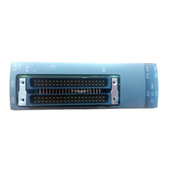
Page 22: Names
3-3 Names 3-3-1 NP1F-MP1 (for 1 axis) EMG+OT-OT 1) Status indication LED 2) External I/O signal connector 1) Status indication LED This LED indicates the operation status and the error status of NP1F-MP1. LED color means as shown below. • Green: This is used to confirm the operation, not emergency. •... - Page 23 3-3 Names 2) Connector pin layout for the external I/O signal A front view Signal name Connector pin layout (40-pin) Connector • NP1F-MP1 side Connector ··· FCN-365P040-AU (Fujitsu) ··· FCN-360A2 (Fujitsu) For details of the connector, refer to “4-6 I/O Wiring.” *1 Manual pulse unit GND (B3, B4) are connected internal.
-
Page 24: Np1F-Mp2 (For 2 Axes)
3-3 Names 3-3-2 NP1F-MP2 (for 2 axes) ONL RDY EMG+OT-OT 1) Status indication LED ERR ALM 2) External I/O signal connector CH1 CH2 1) Status indication LED This LED indicates the operation status and the error status of NP1F-MP2. LED color means as shown below. •... - Page 25 3-3 Names 2) Connector pin layout for the external I/O signal A front view A front view Usable connector · NP1F-MP2 side Connector ··· FCN-365P040-AU (Fujitsu) ··· FCN-360A2 (Fujitsu) For details of the connector, refer to “4-6 I/O Wiring.” Connector pin layout (40-pin) Connector pin layout (40-pin) Signal name Signal name...
-
Page 26: Np2F-Lev (Signal Converter)
3-3 Names 3-3-3 NP2F-LEV (Signal converter) 1) Status indication LED 2) External I/O signal connector 1) Status indication LED Status indication LED of NP2F-LEV 2) Connector pin layout for the external I/O signal A front view (the upper side) A front view (the lower side) Connector pin layout (9-pin) Connector pin layout (16-pin) Usable connector... - Page 27 3-3 Names Signal name Signal name l a i l a i l a i l a i l a i l a i l a i l a i...
-
Page 28: Dimensions
3-4 Dimensions 3-4-1 NP1F-MP1 (for 1 axis) 3-4-2 NP1F-MP2 (for 2 axes) (75) (46.5) 3-10... -
Page 29: Np2F-Lev (Signal Converter)
3-4 Dimensions 3-4-3 NP2F-LEV (Signal converter) 39.8 (36) 29.8 (47.2) Ø6 3-11... -
Page 30: Section 4 Wiring
Section 4 Wiring Page 4-1 Mounting Precautions ....................4-1 4-1-1 Number of mountable modules (NP1F-MP1/ NP1F-MP2) ............ 4-1 4-1-2 Wiring precautions ........................ 4-2 4-1-3 Wiring example of the external wiring connector ..............4-2 (1) Connector type ............................4-2 (2) Connector cover type ..........................4-2 4-2 Connector Pin Layout for the External Connection (NP1F-MP1) ...... -
Page 31: Mounting Precautions
Section 4 Wiring 4-1 Mounting Precautions 4-1-1 Number of mountable modules (NP1F-MP1/ NP1F-MP2) To mount the NP1F-MP1 or the NP1F-MP2 to the base board where the CPU module and the power supply module are mounted on, take the following precautions. (1) The number of mountable modules to the base board in MICREX-SX is shown below. -
Page 32: Wiring Precautions
4-1 Mounting Precautions 4-1-2 Wiring precautions Precautions of wiring the positioning control module and the external device are shown below. 1) The cable length between the positioning control module and the driver varies with the driver type. Confirm the specifications of the driver. 2) I/O wiring •... -
Page 33: Connector Pin Layout For The External Connection (Np1F-Mp1)
4-2 Connector Pin Layout for the External Connection (NP1F-MP1) Signal name Connector pin layout (40-pin) Usable connector · NP1F-MP1 side Connector···FCN-365P040-AU (Fujitsu) ···FCN-360A2 (Fujitsu) *For details of usable connector, refer to “4-6 I/O Wiring.” *1 Manual pulse unit GND (B3, B4) are connected internal. *2 Feedback pulse GND (A5, B5) are connected internal. -
Page 34: External I/O Signal Specifications (Np1F-Mp1)
4-2 Connector Pin Layout for the External Connection (NP1F-MP1) 4-2-1 External I/O signal specifications (NP1F-MP1) t i s... -
Page 35: External I/O Signal Interface (Np1F-Mp1)
4-2 Connector Pin Layout for the External Connection (NP1F-MP1) 4-2-2 External I/O signal interface (NP1F-MP1) Signal name Circuit Manual pulse unit command signal Manual pulse Phase-A 120Ω unit side 220Ω 1.2kΩ Phase-A 120Ω Phase-B 120Ω 220Ω 1.2kΩ Phase-B 120Ω CH1 side When the manual pulse unit utilizes open collectors. - Page 36 4-2 Connector Pin Layout for the External Connection (NP1F-MP1) Signal name Circuit Feedback pulse signal Phase-A 120Ω Servo side 220Ω 1.2kΩ 120Ω Phase-A Phase-B 120Ω 220Ω 1.2kΩ 120Ω Phase-B Phase-Z 120Ω 220Ω 1.2kΩ 120Ω Phase-Z CH1 side When the feedback pulse signal is driven by a open collector. Servo side Phase-A 120Ω...
- Page 37 4-2 Connector Pin Layout for the External Connection (NP1F-MP1) Signal name Circuit External input signal +24V 820Ω 3.9kΩ 820Ω 3.9kΩ 820Ω 3.9kΩ Emergency stop 820Ω 3.9kΩ Origin LS 820Ω 3.9kΩ Interrupt CH1 side Pulse output signal CH1 side Servo side When the servo device utilizes open collectors...
- Page 38 4-2 Connector Pin Layout for the External Connection (NP1F-MP1) Signal name Circuit External output signal +24V 3.9kΩ 3.9kΩ CH1 side...
-
Page 39: Connector Pin Layout For The External Connection (Np1F-Mp2)
4-3 Connector Pin Layout for the External Connection (NP1F-MP2) Connector pin layout (40-pin) Usable connector · NP1F-MP2 side Connector ··· FCN-365P040-AU (Fujitsu) ··· FCN-360A2 (Fujitsu) For details of usable connector, refer to “4-6 I/O Wiring.” Signal name Signal name *1 Manual pulse unit GND (B3, B4) are connected internal. *2 Do not use NC terminals as repeating terminals. -
Page 40: External I/O Signal Specifications (Np1F-Mp2)
4-3 Connector Pin Layout for the External Connection (NP1F-MP2) *5 For output: 24V DC (A13, B13) are connected internal. *6 0V DC (A19, B19) are connected internal. *7 24V DC (A20, B20) are connected internal. *8 Input COM1 (A14, B14, B15) are connected internal. (Input COM1 and Input COM2 are not connected.) *9 Input COM2 (A14, B14, B15) are connected internal. -
Page 41: External I/O Signal Interface (Np1F-Mp2)
4-3 Connector Pin Layout for the External Connection (NP1F-MP2) 4-3-2 External I/O signal interface (NP1F-MP2) Signal name Circuit Manual pulse unit command signal Manual pulse Phase-A 120Ω unit side 220Ω 1.2kΩ Phase-A 120Ω Phase-B 120Ω 220Ω 1.2kΩ Phase-B 120Ω CH1 side When the manual pulse unit utilizes open collectors. - Page 42 4-3 Connector Pin Layout for the External Connection (NP1F-MP2) Signal name Circuit Feedback pulse signal Phase-A 120Ω Servo side 220Ω 1.2kΩ 120Ω Phase-A Phase-B 120Ω 220Ω 1.2kΩ 120Ω Phase-B Phase-Z 120Ω 220Ω 1.2kΩ 120Ω Phase-Z CH1 side Phase-A 120Ω Servo side 220Ω...
- Page 43 4-3 Connector Pin Layout for the External Connection (NP1F-MP2) Signal name Circuit Feedback pulse signal Servo side Phase-A 120Ω Phase-A 220Ω 1.2kΩ 120Ω Phase-B 120Ω Phase-B 220Ω 1.2kΩ 120Ω Phase-Z 120Ω Phase-Z 220Ω 1.2kΩ 120Ω CH1 side Servo side Phase-A 120Ω...
- Page 44 4-3 Connector Pin Layout for the External Connection (NP1F-MP2) Signal name Circuit External input signal +24V CH1-A14 820Ω 3.9kΩ CH1-B16 820Ω 3.9kΩ CH1-B17 820Ω 3.9kΩ CH1-A17 Emergency stop 820Ω 3.9kΩ CH1-A16 Origin LS 820Ω 3.9kΩ CH1-A15 Interrupt CH1 side +24V CH2-A14 820Ω...
- Page 45 4-3 Connector Pin Layout for the External Connection (NP1F-MP2) Signal name Circuit Pulse output signal CH1 side Servo side CH2 side Servo side When the servo device utilizes open collectors. 4-15...
- Page 46 4-3 Connector Pin Layout for the External Connection (NP1F-MP2) Signal name Circuit +24V External output signal 3.9kΩ 3.9kΩ CH1 side +24V 3.9kΩ 3.9kΩ CH2 side 4-16...
-
Page 47: Connector Pin Layout For The External Connection (Signal Converter)
4-4 Connector Pin Layout for the External Connection (Signal Converter) A front view (the upper side) Signal name Connector pin layout (9-pin) Usable connector • NP2F-LEV side Connector···DELC-J9SAF-13L6 (JAE made) Use the following connector and cover. Connector ··· DE-9P-N (JAE made) Cover ··········... -
Page 48: External I/O Signal Specifications (Signal Converter)
4-4 Connector Pin Layout for the External Connection (Signal Converter) 4-4-1 External I/O signal specifications (Signal converter) Ω µ µ 4-18... -
Page 49: External I/O Signal Interface (Signal Converter)
4-4 Connector Pin Layout for the External Connection (Signal Converter) 4-4-2 External I/O signal interface (Signal converter) Signal name Circuit Input side connector (9-pin) 220Ω 10kΩ 390Ω 220Ω 10kΩ 390Ω 220Ω 10kΩ CH1 side 390Ω (Pulse output) 220Ω 10kΩ 390Ω Converter side 4-19... - Page 50 4-4 Connector Pin Layout for the External Connection (Signal Converter) Signal name Circuit Output side connector (16-pin) Servo side +24V Connector side 4-20...
-
Page 51: Connecting
4-5 Connecting 4-5-1 Connecting sample of a servo motor The relationship between the pulse generated by the NP1F-MP1 or the NP1F-MP2 and the rotation of a servo motor is as shown below. Note: Forward rotation and reverse rotation of the FUJI’s servo motor are reserved for other manufactures. The direction indication of the motor rotation is the shaft view from the motor mounted side. -
Page 52: Connecting Sample Of Faldic-Ii And Np1F-Mp2
4-5 Connecting (3) Connecting sample of FALDIC-II and NP1F-MP2 Pulse train positioning control combined module Servo amplifier Servo motor RYG***HA-VV GRH***BG-** NP1F-MP2 Forward pulse output Pulse output COM Reverse pulse output Motor Pulse output COM Feedback pulse DC5V phase-A Feedback pulse *phase-A Feedback pulse phase-B... -
Page 53: Connecting Sample Of A Stepping Motor And Np1F-Mp2
4-5 Connecting (4) Connecting sample of a stepping motor and NP1F-MP2 Pulse train positioning control combined module Stepping motor NP1F-MP2 driver Forward pulse output Pulse output Reverse pulse +CCW output Pulse output -CCW Feedback pulse phase-Z Feedback pulse *phase-Z Stepping motor Feedback pulse Feedback pulse BLACK... -
Page 54: I/O Wiring
4-6 I/O Wiring • I/O wiring depends on the module type, connected external devices, electrical specifications and the environment. (1) Wiring of a connector type module Usable connector and applicable cable size are shown below. Soldered type 4-24... -
Page 55: Section 5 Memory Map
Section 5 Memory Map Page 5-1 NP1F-MP1/NP1F-MP2 Memory Map (Internal Memory List) ........5-1 5-2 NP1F-MP1 I/O Area ..................... 5-2 5-2-1 NP1F-MP1 (read area: address No. 0 to No. 9) ..............5-3 (1) Bit data signal (status signal, address No. “0,” lower word) ..............5-3 (2) Bit data signal (Status signal, address No. -
Page 56: Np1F-Mp1/Np1F-Mp2 Memory Map (Internal Memory List)
Section 5 Memory Map 5-1 NP1F-MP1/NP1F-MP2 Memory Map (Internal Memory List) The memory map for the NP1F-MP1/NP1F-MP2 is shown below. Data is passed from the CPU via an SX bus and I/O area (I/Q area). [CPU program] SX bus I/O area (occupies 22/14 words) t s i t s i... -
Page 57: Np1F-Mp1 I/O Area
5-2 NP1F-MP1 I/O Area The NP1F-MP1I/O area (I/Q area) is shown below: Address No. Remarks lower word Bit data signal PC < = = MP1 upper word Bit data signal PC < = = MP1 lower word Current value read PC <... -
Page 58: Np1F-Mp1 (Read Area: Address No. 0 To No. 9)
5-2 NP1F-MP1 I/O Area 5-2-1 NP1F-MP1 (read area: address No. 0 to No. 9) (1) Bit data signal (status signal, address No. “0,” lower word) " " e l i " " e l i t s i " " 0 t i s "... - Page 59 5-2 NP1F-MP1 I/O Area 1) Description of individual signal names <Description> • This signal is “1” while the deviation amount is within the setting range of the near-zero monitoring register. Absolute value of the deviation amount ≤ Near-zero monitoring register Precaution: Because the deviation amount is always “0”...
- Page 60 5-2 NP1F-MP1 I/O Area <Description> • In the pulse generation mode, this signal becomes “1” when the positioning operation has ended. This signal also becomes “1” when command pulse output is stopped or when the near-zero signal is “1” and the start command signal is “0.”...
- Page 61 5-2 NP1F-MP1 I/O Area <Description> • Indicates which direction to output the command pulse in.“0”: Forward; “1”: Reverse The bit data for the rotation direction is changed over when pulse output is started by the start command. • In the pulse generation mode, this signal changes when command pulse output is started but does not change while the pulse is being output or pulse output is stopped.
- Page 62 5-2 NP1F-MP1 I/O Area <Description> • This is a response signal to the current value counter reset command or command pulse register reset command in the pulse generation mode. This signal becomes “1” while the current value counter reset command or command pulse register reset command is “1.”...
- Page 63 5-2 NP1F-MP1 I/O Area <Description> • In the pulse generation mode or position command mode, this signal becomes “1” when the interrupt signal is detected after the interrupt position detect command has become “1.” While this signal is “1,” the deviation amount data when the interrupt signal was detected or the lower word of the current value counter when the interrupt signal was detected is output in the current value data area (address No.
- Page 64 5-2 NP1F-MP1 I/O Area <Description> • In the pulse generation mode or position command mode, this signal becomes “1” when it is detected that the emergency stop input signal has become “OFF.” After the emergency stop input signal has been returned to the normal state, when the rising edge at which the command pulse register reset signal changes from “0”...
- Page 65 5-2 NP1F-MP1 I/O Area <Description> • When the -OT signal is enabled in the pulse generation mode or position command mode, this signal becomes “1” the moment the -OT input signal becomes “OFF” and an -OT error is detected. After the -OT input signal has been returned to the normal state, when the rising edge at which the command pulse register reset signal changes from “0”...
- Page 66 5-2 NP1F-MP1 I/O Area <Description> • In the pulse generation mode or position command mode, when the error monitoring signal does not change for a given period of time (which is set in the error monitoring timer register), this signal becomes “1.” When the rising edge at which the command pulse register reset signal changes from “0”...
-
Page 67: Bit Data Signal (Status Signal, Address No. 1, Upper Word)
5-2 NP1F-MP1 I/O Area (2) Bit data signal (Status signal, address No. 1, upper word) " " 1 " " 1 " " 1 " " 1 " " 1 " " 1 " " 1 z i l ) t i t s i t s i t s i... - Page 68 5-2 NP1F-MP1 I/O Area <Description> • This signal is changed from “0” to “1” according to the external input signal level of this module. Dedicated functions are assigned to input signals DI1 to DI5. When the dedicated functions are not used, DI2 to DI5 can be used as general-purpose inputs. DI1: Emergency stop input (NC contact input) DI2: +OT input (NC contact input) DI3: -OT input (NC contact input)
- Page 69 5-2 NP1F-MP1 I/O Area <Description> • This is a read register select command signal.While the response signal to the data read command is “0,” read register select data is output to this area. Also, while the response signal to the data read command is “1,” the data in the current data area changes dynamically.
- Page 70 5-2 NP1F-MP1 I/O Area ) l l <Description> • In the pulse generation mode, positioning data can be stored in up to 4 stages. This signal becomes “1” when the buffer to store positioning data is full. While this signal is “1,” no data is stored in the FIFO buffer. Register select Target frequency No.
-
Page 71: Current Value Read (Address No. 2: Lower Word; Address No. 3: Upper Word)
5-2 NP1F-MP1 I/O Area (3) Current value read (Address No. 2: lower word; address No. 3: upper word) The numeric data which is output in this area is selected by the bit command sent from the CPU module. " " 1 "... -
Page 72: Module Detection Time (Address No. 9)
5-2 NP1F-MP1 I/O Area (6) Module detection time (Address No. 9) • Module detection time data output area Module output time is the time measured by in µs since transmission end interrupt was made on the SX bus until periodic processing is started on the module. SX bus send end Module... -
Page 73: Np1F-Mp1 (Write Area: Address Nos. 10 To 13)
5-2 NP1F-MP1 I/O Area 5-2-2 NP1F-MP1 (Write area: address Nos. 10 to 13) (1) Bit command signal (write signal, address No. 10, lower word) 0 " " , 1 " " , t i s t s i e l i "... - Page 74 5-2 NP1F-MP1 I/O Area <Description> • In the pulse generation mode, the pulse train is output when the rising edge at which this signal changes from “0” to “1” is detected. The command pulse zero signal becomes “1” when pulse output ends. After pulse output has ended, when near-zero is detected, the positioning end signal becomes “1.”...
- Page 75 5-2 NP1F-MP1 I/O Area <Description> • When phase-Z (or interrupt signal) is detected, the signal to be output to the current value data area (address No. 3) is selected. “0”: The deviation amount when phase-Z (or interrupt signal) was detected “1”: The lower word of current value counter when phase-Z (or interrupt signal) was detected <Description>...
- Page 76 5-2 NP1F-MP1 I/O Area <Description> • In the pulse generation mode, while this signal is “1,” the set value data is continuously written in the target frequency register. Speed change command “1” (PC = = > MP1) Speed changing “1” (PC <...
- Page 77 5-2 NP1F-MP1 I/O Area <Description> • When the first phase-Z signal is detected after this signal has become “1,” the phase-Z detect bit data signal becomes “1.” In the current value data area (address No. 3), the deviation amount data or the lower word of the current value counter when phase-Z was detected is output.
- Page 78 5-2 NP1F-MP1 I/O Area <Description> • In the pulse generation mode, when the first interrupt signal is detected after this signal has become “1,” the bit data signal for interrupt signal detection becomes “1.” At the same time, the deviation amount data or the lower word of the current value counter when the interrupt signal was detected is output in the current value data area (address No.
- Page 79 5-2 NP1F-MP1 I/O Area <Description> • In the pulse generation mode, interrupt mode is enabled when this signal is “1” at the rising edge of the start signal. In interrupt mode, after a change is detected in the specified signal, the specified number of pulses are output. Interrupt mode is used for original point return motion, interrupt positioning motion or manual operation (infinite length).
- Page 80 5-2 NP1F-MP1 I/O Area Example of interrupt position detection Set value of command pulse register Time (t) Interrupt mode “1” (PC = = > MP1) Start command “1” (PC = = > MP1) Positioning end “1” “1” (PC < = = MP1) Command pulse zero “1”...
- Page 81 5-2 NP1F-MP1 I/O Area <Description> • While the external pulse interrupt position detect command is “1,” external pulse interrupt signal detection is enabled. <Description> • In the pulse generation mode, when this signal becomes “1,” operation is decelerated and then stopped according to the set values of acceleration/deceleration register 1.
- Page 82 5-2 NP1F-MP1 I/O Area <Description> • In the pulse generation mode, when this signal becomes “1,” operation is stopped quickly according to the set values of acceleration/deceleration register 2. Even when this signal becomes “0” during the processing for deceleration, the processing for stop is continued. While this signal is “1,”...
- Page 83 5-2 NP1F-MP1 I/O Area <Description> • The alarm detect signal is reset at the rising edge at which this signal changes from “0” to “1.” Alarm reset “1” (PC = = > MP1) Alarm detection “1” (PC < = = MP1) Precautions: Alarm detect signal is valid for the following errors: ·...
- Page 84 5-2 NP1F-MP1 I/O Area <Description> • In the pulse generation mode, when an error has been detected, pulse output is stopped and DO output signal is turned OFF. • If pulse output has been stopped when an error is detected, DO output is immediately turned OFF. •...
-
Page 85: Bit Command Signal (Write Signal, Address No. 11, Upper Word)
5-2 NP1F-MP1 I/O Area (2) Bit command signal (Write signal, address No. 11, upper word) t s i t s i 1) Write register select Description Bit No. 0 to 4 Target frequency register Base frequency register Current frequency register Command pulse register Deceleration point register Acceleration/deceleration register 1... - Page 86 5-2 NP1F-MP1 I/O Area <Description> • Sign signal for the position command data which is sent from the CPU module Sign = “0”: Forward (the direction to increase the current position value) “1”: Reverse (the direction to decrease the current position value) Position command data is 32-bit length with sign (+).
- Page 87 5-2 NP1F-MP1 I/O Area 2) Read register Bit No. Description 8 to 12 Target frequency register Base frequency register Current frequency register Command pulse register Deceleration point register Acceleration/deceleration register 1 Acceleration/deceleration register 2 Speed multiplication register Command pulse counter Target frequency FIFO buffer Command pulse register FIFO buffer (Not used)
- Page 88 5-2 NP1F-MP1 I/O Area <Description> • While this signal is “1,” the content of the selected register is output in the current value data area. At the same time, the response to the data read command becomes “1.” Register select (PC = = >...
-
Page 89: Set Value Area (Write Signal, Address Nos. 12 And 13)
5-2 NP1F-MP1 I/O Area (3) Set value area (Write signal, address Nos. 12 and 13) Precautions: • Numeric data is treated as binary data. • Effective number of bits is determined by the bit-width of each register. The part exceeding the bit-width of each register is ignored. •... -
Page 90: I/O Area Of Np1F-Mp2
5-3 I/O Area of NP1F-MP2 The I/O area (I/Q area) of the NP1F-MP2 is shown below: Address No. Remarks lower word Ch1 Bit data signal PC < = = MP2 upper word Ch1 Bit data signal PC < = = MP2 lower word Ch1 Current value data 1 PC <... -
Page 91: Np1F-Mp2 (Read Area: Address No. 0 To No. 13)
5-3 I/O Area of NP1F-MP2 5-3-1 NP1F-MP2 (Read area: address No. 0 to No. 13) (1) Ch1 bit data signal (Status signal, address No. 0, lower word) " " e l i " " e l i t s i "... - Page 92 5-3 I/O Area of NP1F-MP2 <Description> • In pulse generation mode, the status of this signal becomes “1” (one) when the “command pulse register” is “0” (zero) and the FIFO buffer is cleared. The command pulse register becomes “1” when pulse output is completed, when the command pulse register reset command is issued.
- Page 93 5-3 I/O Area of NP1F-MP2 <Description> • In the pulse generation mode, this signal becomes “1” when the positioning operation has ended. This signal also becomes “1” when command pulse output is stopped or when the near-zero signal is “1” and the start command signal is “0.”...
- Page 94 5-3 I/O Area of NP1F-MP2 <Description> • Indicates which direction to output the command pulse in. “0”: forward; “1”: reverse The bit data for the direction of rotation is changed over when pulse output is started by the start command. •...
- Page 95 5-3 I/O Area of NP1F-MP2 <Description> • This is a response signal to the current value counter reset command or command pulse register reset commands in the pulse generation mode. This signal becomes “1” while the current value counter reset command or command pulse register reset command is “1.”...
- Page 96 5-3 I/O Area of NP1F-MP2 <Description> • In the pulse generation mode or position command mode, this signal becomes “1” when an effective phase-Z signal is detected after the phase-Z signal detect command has become “1.” While this signal is “1,” the deviation amount data when phase-Z was detected or the lower word of the current value counter when phase-Z was detected is output in current value data area 2.
- Page 97 5-3 I/O Area of NP1F-MP2 <Description> • In the pulse generation mode, this signal becomes “1” while the accelerating/decelerating operation is being executed by this module (while the frequency of the command pulse is changing). Time Start command “1” (PC = = > MP2) Positioning end “1”...
- Page 98 5-3 I/O Area of NP1F-MP2 <Description> • In the pulse generation mode or position command mode, this signal becomes “1” when it is detected that the emergency stop input signal has become “OFF.” After the emergency stop input signal has been returned to the normal state, when the rising edge at which the command pulse register reset signal changes from “0”...
- Page 99 5-3 I/O Area of NP1F-MP2 <Description> • When the -OT signal is enabled in the pulse generation mode or position command mode, this signal becomes “1” when the -OT input signal becomes “OFF” and an -OT error is detected. After the -OT input signal has been returned to the normal state, when the rising edge at which the command pulse register reset signal changes from “0”...
- Page 100 5-3 I/O Area of NP1F-MP2 <Description> • In the pulse generation mode or position command mode, when the error monitoring signal does not change for a given period of time (which is set in the error monitoring timer register), this signal becomes “1.” When the rising edge at which the command pulse register reset signal changes from "0"...
-
Page 101: Ch1 Bit Data Signal (Status Signal, Address No. 1, Upper Word)
5-3 I/O Area of NP1F-MP2 (2) Ch1 bit data signal (Status signal, address No. 1, upper word) " " 1 " " 1 " " 1 " " 1 " " 1 " " 1 " " 1 z i l t s i ) t i t s i... - Page 102 5-3 I/O Area of NP1F-MP2 <Description> • This signal is changed from “0” to “1” according to the external input signal level of this module. Dedicated functions are assigned to input signals DI1 to DI5. When the dedicated functions are not used, DI2 to DI5 can be used as general-purpose inputs. DI1: Emergency stop input (NC contact input) DI2: +OT input (NC contact input) DI3: -OT input (NC contact input)
- Page 103 5-3 I/O Area of NP1F-MP2 <Description> • This is a read register select command signal While the response signal to the data read command is “0,” read register select data is output to this area. Also, while the response signal to the data read command is “1,” the data in the current data areas 1 and 2 changes dynamically.
- Page 104 5-3 I/O Area of NP1F-MP2 ) l l <Description> • In the pulse generation mode, positioning data can be stored in up to 4 stages. This signal becomes “1” when the buffer to store positioning data is full. While this signal is “1,” no data is stored in the FIFO buffer. Register select Target frequency No.
-
Page 105: Ch1 Current Value Read (Address No. 2: Lower Word; Address No. 3: Upper Word)
5-3 I/O Area of NP1F-MP2 (3) Ch1 current value read (Address No. 2: lower word; address No. 3: upper word) The numeric data which is output in this area is selected by the bit command sent from the CPU module. "... -
Page 106: Ch2 Bit Data Signal (Status Signal, Address No. 6, Lower Word)
5-3 I/O Area of NP1F-MP2 (5) Ch2 bit data signal (Status signal, address No. 6, lower word) " " e l i " " e l i t s i " " 0 t i s " " t i s "... - Page 107 5-3 I/O Area of NP1F-MP2 1) Description of individual signal names <Description> • This signal becomes “1” while the deviation amount is within the setting range of the near-zero monitoring register. Absolute value of the deviation amount ≤ Near-zero monitoring register Precaution: Because the deviation amount is always “0”...
- Page 108 5-3 I/O Area of NP1F-MP2 <Description> • In the pulse generation mode, this signal becomes “1” when the positioning operation has ended. This signal also becomes “1” when command pulse output is stopped or when the near-zero signal is “1” and the start command signal is “0.”...
- Page 109 5-3 I/O Area of NP1F-MP2 <Description> • Indicates which direction to output the command pulse in.“0”: Forward; “1”: Reverse The bit data for the direction of rotation is changed over when pulse output is started by the start command. • In the pulse generation mode, this signal changes when command pulse output is started but does not change while pulse is being output or pulse output is stopped.
- Page 110 5-3 I/O Area of NP1F-MP2 <Description> • This is a response signal to the current value counter reset command or command pulse register reset command in the pulse generation mode. This signal becomes “1” while the current value counter reset command or command pulse register reset command is “1.”...
- Page 111 5-3 I/O Area of NP1F-MP2 <Description> • In the pulse generation mode or position command mode, this signal becomes “1” when an effective phase-Z signal is detected after the phase-Z signal detect command has become “1.” While this signal is “1,” the deviation amount data when phase-Z was detected in current value data area 2 or the lower word of the current value counter when phase-Z was detected is output.
- Page 112 5-3 I/O Area of NP1F-MP2 <Description> • In the pulse generation mode, this signal becomes “1” while the accelerating/decelerating operation is being executed by this module (while the frequency of command pulse is changing). Time Start command “1” (PC = = > MP2) Positioning end “1”...
- Page 113 5-3 I/O Area of NP1F-MP2 <Description> • In the pulse generation mode or position command mode, this signal becomes “1” when it is detected that the emergency stop input signal has become “OFF.” After the emergency stop input signal has been returned to the normal state, when the rising edge at which the command pulse register reset signal changes from “0”...
- Page 114 5-3 I/O Area of NP1F-MP2 <Description> • When the -OT signal is enabled in the pulse generation mode or position command mode, this signal becomes “1” the moment the -OT input signal becomes “OFF” and an -OT error is detected. After the -OT input signal has been returned to the normal state, when the rising edge at which the command pulse register reset signal changes from “0”...
- Page 115 5-3 I/O Area of NP1F-MP2 <Description> • In the pulse generation mode or position command mode, this signal becomes “1” when the deviation amount is out of the setting range of “deviation over monitoring register.” After the deviation amount has been reset by the deviation amount reset signal, and the rising edge at which alarm reset signal changes from “0”...
-
Page 116: Ch2 Bit Data Signal (Status Signal, Address No. 7, Upper Word)
5-3 I/O Area of NP1F-MP2 (6) Ch2 bit data signal (status signal, address No. 7, upper word) " " 1 " " 1 " " 1 " " 1 g i r " " 1 " " 1 " " 1 i n i a i t z i l... - Page 117 5-3 I/O Area of NP1F-MP2 <Description> • This signal becomes “1” when processing for initialization has ended normally. After this, the signal continues to be “1.” Precaution: This signal becomes “0” while a deviation-over error is detected. t i r <Description>...
- Page 118 5-3 I/O Area of NP1F-MP2 <Description> • A read register select command signal. While the response signal to the data read command is “0,” read register select data is output to this area. Also while the response signal to the data read command is “1,” data in the current data areas 1 and 2 change dynamically.
- Page 119 5-3 I/O Area of NP1F-MP2 ) l l <Description> • In the pulse generation mode, positioning data can be stored in up to 4 stages. This signal becomes “1” when the buffer to store positioning data is full. While this signal is “1,” no data is stored in the FIFO buffer. Register select Target frequency No.
-
Page 120: Current Value Read (Address No. 8: Lower Word; Address No. 9: Upper Word)
5-3 I/O Area of NP1F-MP2 (7) Current value read (Address No. 8: lower word; address No. 9: upper word) The numeric data which is output in this area is selected by the bit command sent from the CPU module. " "... -
Page 121: Module Detection Time (Address No. 13)
5-3 I/O Area of NP1F-MP2 (10) Module detection time (Address No. 13) • This is the module detection time data output area. Module output time is the time measured in µs since transmission end interrupt was made on the SX bus until periodic processing is started on the module. -
Page 122: Np1F-Mp2 (Write Area: Address Nos. 14 To 21)
5-3 I/O Area of NP1F-MP2 5-3-2 NP1F-MP2 (Write area: address Nos. 14 to 21) (1) Ch1 bit command signal (Write area, address No. 14, lower word) 0 " " , 1 " " , t i s e l i "... - Page 123 5-3 I/O Area of NP1F-MP2 <Description> • In the pulse generation mode, the pulse train is output when the rising edge at which this signal changes from “0” to “1” is detected. The command pulse zero signal becomes “1” when pulse output ends. After pulse output has ended, when near-zero is detected, the positioning end signal becomes “1.”...
- Page 124 5-3 I/O Area of NP1F-MP2 <Description> • When phase-Z (or interrupt signal) is detected, the signal to be output to current value data area 2 is selected. “0”: The deviation amount when phase-Z (or interrupt signal) was detected “1”: The lower word of the current value counter when phase-Z (or interrupt signal) was detected <Description>...
- Page 125 5-3 I/O Area of NP1F-MP2 <Description> • In the pulse generation mode, while this signal is “1,” set value data is continuously written in the target frequency register. Speed change command “1” (PC = = > MP2) Speed changing “1” (PC <...
- Page 126 5-3 I/O Area of NP1F-MP2 <Description> • When the first phase-Z signal is detected after this signal has become “1,” the bit data signal for phase-Z detection becomes “1.” In current value data area 2, the deviation amount data or the lower word of the current value counter at the moment phase-Z was detected is output.
- Page 127 5-3 I/O Area of NP1F-MP2 <Description> • In the pulse generation mode, when the first interrupt signal is detected after this signal has become “1,” the bit data signal for interrupt signal detection becomes “1.” At the same time, the deviation amount data or the lower word of the current value counter at the moment the interrupt signal was detected is output in current value data area 2.
- Page 128 5-3 I/O Area of NP1F-MP2 <Description> • In the pulse generation mode, interrupt mode is enabled when this signal is “1” at the rising edge of the start signal. In interrupt mode, after a change is detected in the specified signal, the specified number of pulses are output. Interrupt mode is used for original point return motion, interrupt positioning motion or manual operation (infinite length).
- Page 129 5-3 I/O Area of NP1F-MP2 Example of interrupt position detection Set value of command pulse register Time (t) Interrupt mode “1” (PC = = > MP2) Start command “1” (PC = = > MP2) Positioning end “1” “1” (PC < = = MP2) Command pulse zero “1”...
- Page 130 5-3 I/O Area of NP1F-MP2 <Description> • <Description> • In the pulse generation mode, when this signal becomes “1,” operation is decelerated and then stopped according to the set values of acceleration/deceleration register 1. Even when this signal becomes “0” during processing for deceleration, the processing for stopping is continued. While this signal is “1,”...
- Page 131 5-3 I/O Area of NP1F-MP2 <Description> • In the pulse generation mode, when this signal becomes “1,” operation is stopped quickly according to the set values of acceleration/deceleration register 2. Even when this signal becomes “0” during processing for quickly, the processing for stopping is continued. While this signal is “1,”...
- Page 132 5-3 I/O Area of NP1F-MP2 <Description> • The alarm detect signal is reset at the rising edge at which this signal changes from “0” to “1.” Alarm reset “1” (PC = = > MP2) Alarm detection “1” (PC < = = MP2) Precautions: The alarm detect signal is valid for the following errors: ·...
- Page 133 5-3 I/O Area of NP1F-MP2 <Description> • In the pulse generation mode, when an error is detected, pulse output is stopped and DO output signal is turned OFF. If pulse output has been stopped when an error is detected, DO output is immediately turned OFF. If command pulse is being output when an error is detected, operation is decelerated and then stopped by acceleration/deceleration register 2.
-
Page 134: Ch1 Bit Command Signal (Write Signal, Address No. 15, Upper Word)
5-3 I/O Area of NP1F-MP2 (2) Ch1 bit command signal (Write signal, address No. 15, upper word) t s i t s i 1) Write register select Bit No. Description 0 to 4 Target frequency register Base frequency register Current frequency register Command pulse register Deceleration point register Acceleration/deceleration register 1... - Page 135 5-3 I/O Area of NP1F-MP2 <Description> • This is the sign signal for the position command data which is sent from the CPU module Sign = “0”: Forward (direction to increase the current position value) “1”: Reverse (direction to decrease the current position value) Position command is 32-bit-length signed data (+).
- Page 136 5-3 I/O Area of NP1F-MP2 2) Read register Bit No. Description 8 to 12 Target frequency register Base frequency register Current frequency register Command pulse register Deceleration point register Acceleration/deceleration register 1 Acceleration/deceleration register 2 Speed multiplication register Command pulse counter Target frequency FIFO buffer Command pulse register FIFO buffer (Not used)
-
Page 137: Ch1 Set Value Area (Write Signal, Address Nos. 16 And 17)
5-3 I/O Area of NP1F-MP2 <Description> • While this signal is “1,” the content of selected register is output in current value data area 1 or 2. At the same time, the response to the data read command becomes “1.” Register select (PC = = >... -
Page 138: Ch2 Bit Command Signal (Write Signal, Address No. 18, Lower Word)
5-3 I/O Area of NP1F-MP2 (4) Ch2 bit command signal (write signal, address No. 18, lower word) 0 " " , 1 " " , t i s e l i " " , " " , " i " f i c t i s "... - Page 139 5-3 I/O Area of NP1F-MP2 <Description> • In the pulse generation mode, the pulse train is output when the rising edge at which this signal changes from “0” to “1” is detected. The command pulse zero signal becomes “1” when pulse output ends. After pulse output has ended, when near-zero is detected, the positioning end signal becomes “1.”...
- Page 140 5-3 I/O Area of NP1F-MP2 <Description> • When phase-Z (or interrupt signal) is detected, the signal to be output to current value data area 2 is selected. “0”: The deviation amount when phase-Z (or interrupt signal) was detected “1”: The lower word of the current value counter when phase-Z (or interrupt signal) was detected <Description>...
- Page 141 5-3 I/O Area of NP1F-MP2 <Description> • In the pulse generation mode, while this signal is “1,” set value data is continuously written in the target frequency register. Speed change command “1” (PC = = > MP2) Speed changing “1” (PC <...
- Page 142 5-3 I/O Area of NP1F-MP2 <Description> • When the first phase-Z signal is detected after this signal has become “1,” the bit data signal for phase-Z detection becomes “1.” In current value data area 2, the deviation amount data or the lower word of the current value counter at the moment phase-Z was detected is output.
- Page 143 5-3 I/O Area of NP1F-MP2 <Description> • In the pulse generation mode, when the first interrupt signal is detected after this signal has become “1,” the bit data signal for interrupt signal detection becomes “1.” At the same time, the deviation amount data or the lower word of the current value counter at the moment the interrupt signal was detected is output in current value data area 2.
- Page 144 5-3 I/O Area of NP1F-MP2 <Description> • In the pulse generation mode, interrupt mode is enabled when this signal is “1” at the rising edge of the start signal. In interrupt mode, after a change is detected in a specified signal, the specified number of pulses are output. Interrupt mode is used for original point return motion, interrupt point positioning motion or manual operation (infinite length).
- Page 145 5-3 I/O Area of NP1F-MP2 Example of interrupt position detection Set value of command pulse register Time (t) Interrupt mode “1” (PC = = > MP2) Start command “1” (PC = = > MP2) Positioning end “1” “1” (PC < = = MP2) Command pulse zero “1”...
- Page 146 5-3 I/O Area of NP1F-MP2 <Description> • <Description> • In the pulse generation mode, when this signal becomes “1,” operation is decelerated and then stopped according to the set values of acceleration/deceleration register 1. Even when this signal becomes “0” during processing for deceleration, the processing for stopping is continued. While this signal is “1,”...
- Page 147 5-3 I/O Area of NP1F-MP2 <Description> • In the pulse generation mode, when this signal becomes “1,” operation is stopped quickly according to the set values of acceleration/deceleration register 2. Even when this signal becomes “0” during processing for quickly, the processing for stopping is continued. While this signal is “1,”...
- Page 148 5-3 I/O Area of NP1F-MP2 <Description> • The alarm detect signal is reset at the rising edge at which this signal changes from “0” to “1.” Alarm reset “1” (PC = = > MP2) Alarm detection “1” (PC < = = MP2) Precautions: Alarm detect signal is valid for the following errors: ·...
- Page 149 5-3 I/O Area of NP1F-MP2 <Description> • In the pulse generation mode, when an error is detected, pulse output is stopped and DO output signal is turned OFF. If pulse output has been stopped when an error is detected, DO output is immediately turned OFF. If command pulse is being output when an error is detected, operation is decelerated and then stopped by acceleration/deceleration register 2.
-
Page 150: Ch2 Bit Command Signal (Write Signal, Address No. 19, Upper Word)
5-3 I/O Area of NP1F-MP2 (5) Ch2 bit command signal (Write signal, address No. 19, upper word) t s i t s i 1) Write register select Bit No. Description 0 to 4 Target frequency register Base frequency register Current frequency register Command pulse register Deceleration point register Acceleration/deceleration register 1... - Page 151 5-3 I/O Area of NP1F-MP2 <Description> • This is the sign signal for the position command data which is sent from the CPU module. Sign = “0”: Forward (direction to increase the current position value) “1”: Reverse (direction to decrease the current position value) Position command is 32-bit-length signed data (+).
- Page 152 5-3 I/O Area of NP1F-MP2 2) Read register Bit No. Description 8 to 12 Target frequency register Base frequency register Current frequency register Command pulse register Deceleration point register Acceleration/deceleration register 1 Acceleration/deceleration register 2 Speed multiplication register Command pulse counter Target frequency FIFO buffer Command pulse register FIFO buffer (Not used)
-
Page 153: Set Value Area (Write Signal, Address Nos. 20 And 21)
5-3 I/O Area of NP1F-MP2 <Description> • While this signal is “1,” the content of selected register is output in current value data area 1 or 2. At the same time, the response to the data read command becomes “1.” Register select (PC = = >... -
Page 154: Setting Method And Effective Bits Of Individual Register
5-4 Setting Method and Effective Bits of Individual Register There are two methods for passing data between the positioning control module and the CPU module: 1) Write data from the CPU module into the positioning control module (Speed data, position data, pulse input method, etc.) 2) Read data from the positioning control module into the CPU module (Current frequency data, maximum frequency data, etc.) 1) When setting by above method 1):... - Page 155 5-4 Setting Method and Effective Bits of Individual Register The number of effective bits is as follows: • Write register Bit No. Description Effective bits 0 to 4 Target frequency register 20-bit length Base frequency register 20-bit length Current frequency register 20-bit length 32-bit length Command pulse register...
- Page 156 5-4 Setting Method and Effective Bits of Individual Register • Read register Bit No. Description Effective bits 8 to 12 Target frequency register 20-bit length Base frequency register 20-bit length Current frequency register 20-bit length Command pulse register 32-bit length Deceleration point register 32-bit length Acceleration/deceleration register 1...
-
Page 157: Section 6 Parameters (Registers)
Section 6 Parameters (Registers) Page 6-1 Parameters List (Registers) ..................6-1 6-2 Relationship between Parameters (Registers) ............6-2 6-3 Detailed Description of Parameters (Registers) ............6-4... - Page 158 Section 6 Parameters (Registers) 6-1 Parameters List (Registers) Internal parameters (registers) of the NP1F-MP1/NP1F-MP2 are listed below: t s i s t i t s i s t i t s i s t i t s i s t i t s i s t i t s i...
-
Page 159: Relationship Between Parameters (Registers)
6-2 Relationship between Parameters (Registers) Relationship between parameters (registers) Target frequency register Speed multiplication register Current frequency register Deceleration point register Base frequency register Speed multiplication register Command pulse register Time Acceleration/deceleration register • Acceleration/deceleration register : Controls acceleration/deceleration time (acceleration). •... - Page 160 6-2 Relationship between Parameters (Registers) The time until maximum output frequency is reached since the NP1F-MP1/NP1F-MP2 has stopped pulse output (0Hz) is calculated from the following formulas. (The minimum setting of acceleration/deceleration register is “1.” Do not set “0.” If “0”...
-
Page 161: Detailed Description Of Parameters (Registers)
6-3 Detailed Description of Parameters (Registers) i t i t s i <Description> • Command pulse frequency (speed) control register • Command pulse is output at the frequency which is set in this register. • Writing is possible at the desired timing. •... - Page 162 6-3 Detailed Description of Parameters (Registers) Precautions: · The write command, from the CPU module into the target frequency register, is enabled only in the pulse generation mode. · Even when the target frequency register is updated during the command pulse output, the automatic computation of the deceleration point is executed.
- Page 163 6-3 Detailed Description of Parameters (Registers) i t i t s i <Description> • Current command pulse frequency control register • Displays the control value of the current command pulse frequency. • The function of the current frequency register differs depending on whether automatic acceleration/deceleration is enabled or disabled.
- Page 164 6-3 Detailed Description of Parameters (Registers) Setting of target frequency register Pulse count at deceleration point Setting of base frequency register Time Start command (PC = = > MP1/MP2) “1” Positioning end “1” “1” (PC < = = MP1/MP2) Current frequency control data Current frequency register (PC <...
- Page 165 6-3 Detailed Description of Parameters (Registers) i t i t s i <Description> • Output pulse count control register (The total number of pulses which are output by a single start command is set.) • By the command pulse, the value of the command pulse register is decremented. Point of use: ·...
- Page 166 6-3 Detailed Description of Parameters (Registers) i t i t s i <Description> • Deceleration point control register • When automatic acceleration/deceleration is enabled, the operation is decelerated to the speed which is set by the base frequency register, according to the value of the deceleration point register and the current value of the command pulse register.
- Page 167 6-3 Detailed Description of Parameters (Registers) 2) When automatic calculation of the deceleration point is disabled • Deceleration point is directly set from the CPU module. Setting of target frequency register Pulse count at deceleration point Setting of base frequency register Time Start command “1”...
- Page 168 6-3 Detailed Description of Parameters (Registers) i t i t s i <Description> • Deceleration time control register (the acceleration for quick stop is set) • Writing is possible at the desired timing. • The setting of the acceleration/deceleration register 2 is enabled only in the pulse generation mode. i t i c i l t s i...
- Page 169 6-3 Detailed Description of Parameters (Registers) i t i <Description> • The frequency (speed) of the positioning data which is to be registered in the FIFO buffer is set. Points of use: · Data cannot be registered in the FIFO buffer only by writing it into the target frequency FIFO buffer. When data is written into the command pulse count FIFO buffer, registration in the FIFO buffer is made in the combination of the frequency and pulse count.
- Page 170 6-3 Detailed Description of Parameters (Registers) i t i i t i i t i i t i t s i <Description> • Transmission error monitor register • Transmission error monitoring time is set. • Influenced by tact time. (A value larger than tact time must be set.) •...
- Page 171 6-3 Detailed Description of Parameters (Registers) i t i t s i <Description> • Control signal to the NP1F-MP1/NP1F-MP2 • Control signal is assigned separately for channels 1 and 2. (For external pulse signal selection, the channel 1 signal is valid.) Point of use: ·...
- Page 172 6-3 Detailed Description of Parameters (Registers) • Detailed explanation of signals in the list 1) Count pulse select (bit 1) Selects enabling/disabling of feedback pulse count. When set to 0 : Feedback pulse is selected (feedback pulse is enabled). : Current value counter counts the number of feedback pulses. When set to 1 : Command pulse is selected (feedback pulse is disabled).
- Page 173 6-3 Detailed Description of Parameters (Registers) 4) +OT detection disable (bit 6) Selects enabling/disabling of the processing under +OT signal input. When set to “0”: Enables the stop operationunder the +OT signal. When set to “1”: Disables the stop operation under the +OT signal. Points of use: ·...
- Page 174 6-3 Detailed Description of Parameters (Registers) 7) Automatic deceleration point calculation disable (bit 9) Selects enabling/disabling of automatic deceleration point calculation. When set to “0”: Enables automatic calculation of the deceleration point. When set to “1”: Disables automaticcalculation of the deceleration point. Points of use: ·...
- Page 175 6-3 Detailed Description of Parameters (Registers) 12) Position command mode (bit 15) • Selects position command mode or pulse generation mode. When bit 15 is “0”: Pulse generation mode When bit 15 is ”1”: Position command mode [Pulse generation mode] •...
- Page 176 6-3 Detailed Description of Parameters (Registers) i t i t s i <Description> • Sets values for the high-speed side command value limiter. • In the pulse generation mode, works as the upper-limit value for frequency register setting data. • In the position command mode, works as the upper-limit value for the increment of pulse count per millisecond. i t i i t i i t i...
- Page 177 6-3 Detailed Description of Parameters (Registers) i t i i t i <Description> • When speed is continuously changed with the speed change command being set to “1,” “pulse count setting buffer, lower” is used to set the number of pulses to be added. •...
- Page 178 6-3 Detailed Description of Parameters (Registers) i t i <Description> • For writing in the pulse count setting buffer, the remaining 12 bits of the set value data area are used. a) Pulse count setting buffer, lower : 12 bits (bit 00 to bit 11) b) Pulse count setting buffer, middle : 12 bits (bit 12 to bit 23) c) Pulse count setting buffer, upper : 8 bits (bit 24 to bit 31)
- Page 179 6-3 Detailed Description of Parameters (Registers) i t i <Description> When speed is changed continuously with the speed change command being set to “1,” this register is used to set the number of pulses to be added. (When data is set in “pulse count setting buffer, 16,” upper one word (16 bits) of the set value data area is added to the command pulse register as the increment of pulse count.) Points of use: ·...
- Page 180 6-3 Detailed Description of Parameters (Registers) i t i t s i <Description> • This register sets the delay time for calculating the increment of the position data sent from the CPU module to output pulses from the pulse generator in position command mode. (The setting of the delay time register is enabled in position command mode.) •...
-
Page 181: Section 7 Positioning Function
Section 7 Positioning Function Page 7-1 Positioning Function of the Pulse Train Positioning Control Combined Module (NP1F-MP1/NP1F-MP2) ................. 7-1 (1) Pulse generation mode ........................... 7-1 (2) Position command mode ........................7-1 7-2 Functions of Each Operation Mode ................7-3 (1) Pulse generation mode ........................... 7-3 (2) Position command mode ........................ - Page 182 Page 7-4-4 Processing when start command is turned OFF ..............7-35 7-4-5 Original point return motion ....................7-35 7-4-6 Interrupt positioning ......................7-35 7-4-7 Operation when an emergency stop error has been detected ..........7-36 7-4-8 Operation when an ± OT error has been detected .............. 7-36 7-4-9 Operation when a transmission error has been detected ...........
- Page 183 Section 7 Positioning Function 7-1 Positioning Function of the Pulse Train Positioning Control Combined Module (NP1F-MP1/NP1F-MP2) • The pulse train positioning control combined module (NP1F-MP1/NP1F-MP2) has the function to detect the current work position by the feedback pulse (current feedback value). Enabling/disabling of the feedback pulse detect function is selected by the control register.
-
Page 184: Positioning Function Of The Pulse Train Positioning Control Combined Module (Np1F-Mp1/Np1F-Mp2)
7-1 Positioning Function of the Pulse Train Positioning Control Combined Module (NP1F-MP1/NP1F-MP2) How to control the position command mode Calculation Calculation 1) Position data set value increment Pulse count data Frequency data Pulse generator Command pulse (step command) Deviation counter Signal Feedback pulse select... -
Page 185: Functions Of Each Operation Mode
7-2 Functions of Each Operation Mode • The pulse train positioning control combined module (NP1F-MP1/NP1F-MP2) has the following two operation modes. (1) Pulse generation mode • This mode is used to set the following items from the CPU module. 1) Moving length (the number of output pulses) 2) Target frequency (2) Position command mode •... -
Page 186: Functions Of Pulse Generation Mode
7-3 Functions of Pulse Generation Mode • Functions of the pulse generation mode are listed below: t i s c i t t i r t s i t s i t i s t i s ± t i s t s i... -
Page 187: Positional Deviation Calculation Function
7-3 Functions of Pulse Generation Mode 7-3-1 Positional deviation calculation function • The method to monitor positional deviation by the pulse train command and feedback pulse count is shown below: Processing for positional deviation monitoring 1) Pulse count data 2) Frequency data Pulse generator (trapezoidal Command pulse... -
Page 188: Command Pulse Count Control
7-3 Functions of Pulse Generation Mode 7-3-2 Command pulse count control • The number of output pulses is controlled by the 32-bit length command pulse register. • The data written into the command pulse register is added to the content of the command pulse register (added as an absolute value without sign). -
Page 189: Command Pulse Frequency Control
7-3 Functions of Pulse Generation Mode 7-3-3 Command pulse frequency control • With the 16/20-bit-length frequency register (target frequency register, base frequency register or current frequency register) and the speed multiplication register, it is possible to control the command pulse frequency or to reference the current frequency value. -
Page 190: Trapezoidal Acceleration/Deceleration
7-3 Functions of Pulse Generation Mode 7-3-4 Trapezoidal acceleration/deceleration • This module (NP1F-MP1/NP1F-MP2) executes the processing for trapezoidal acceleration/deceleration using the acceleration/deceleration register. Acceleration/ deceleration 25MHz 20-bit up/down counter register 1 / n (Current frequency) Decelerate Compare Constant speed Accelerate Target frequency •... - Page 191 7-3 Functions of Pulse Generation Mode Target command frequency Time Acceleration/deceleration time t ≥ 5.2ms (an integrated multiple of 2.6ms) or Acceleration/deceleration time t ≥ 84ms (an integrated multiple of 42ms) Points of use: · To shorten acceleration/deceleration time, decrease the set value of the speed multiplication register and increase the target command frequency.
-
Page 192: Automatic Deceleration Point Calculation
7-3 Functions of Pulse Generation Mode 7-3-5 Automatic deceleration point calculation • When automatic deceleration point calculation is enabled, this module (NP1F-MP1/NP1F-MP2) automatically calculates the deceleration point. Accelerating Deceleration point Decelerating register 32-bit up/down counter Command pulse Comparator Deceleration point signal Command pulse register 32-bit Down counter... -
Page 193: Deceleration Point Setting
7-3 Functions of Pulse Generation Mode 7-3-6 Deceleration point setting • When automatic deceleration point calculation is disabled, the deceleration point needs to be set from the CPU module. In this case, the deceleration point register is not counted up or down, nor cleared to zero when positioning is completed. -
Page 194: Continuous Frequency Rewriting
7-3 Functions of Pulse Generation Mode 7-3-7 Continuous frequency rewriting • The continuous frequency rewriting function continuously writes data from the set value data area into the target frequency register. Speed change command “1” (PC = = > MP1/MP2) Speed changing “1”... -
Page 195: Setting Data To A Register
7-3 Functions of Pulse Generation Mode 7-3-8 Setting data to a register • This function selects a register and writes data in it. Sample setting of frequency data and pulse count data Register select Target frequency register Command pulse register (PC = = >... -
Page 196: Data Reading From Register
7-3 Functions of Pulse Generation Mode 7-3-9 Data reading from register • This function selects a register and reads data from the register into the CPU module. Sample reading of current frequency data and pulse count data Register select Current frequency register Command pulse register (PC = = >... -
Page 197: Current Value Data Reading
7-3 Functions of Pulse Generation Mode 7-3-10 Current value data reading • When the register read command is turned OFF, this function outputs the data of the current value counter into current value data areas 1 and 2. The following are types of current value data, as shown below. Which data to output is selected by the bit command signal sent from the CPU module. -
Page 198: Manual Operation
7-3 Functions of Pulse Generation Mode Remarks: · The increment of the feedback pulse count is calculated using the following formula: Increment of pulse count = Previous read value - Current read value Maximum feedback pulse frequency: 500kHz multiplied by 4 = 2MHz Bit width of counter : 16 bits (when only lower word is used) In the above conditions, the time “t”... -
Page 199: Original Point Return Motion
7-3 Functions of Pulse Generation Mode 7-3-12 Original point return motion • With the interrupt point positioning function and the phase-Z detect function of this module (NP1F-MP1/MP2), it is possible to return to the original point. • Original point return motion is activated when the interrupt detect signal is “1.” •... -
Page 200: Positioning Operation
7-3 Functions of Pulse Generation Mode Points of use: · To use the original point return function with OT in the returning direction or in the reverse direction, or to use the preset function which makes the current position the machine origin, it is necessary to adapt to these functions by the application on the CPU module side. -
Page 201: Interrupt Point Positioning Motion
7-3 Functions of Pulse Generation Mode 7-3-14 Interrupt point positioning motion • When the interrupt signal is detected, this function outputs the specified number of command pulses. • The motion to position at the interrupt starts when the interrupt positioning signal becomes “1.” •... -
Page 202: Deceleration-And-Stop / Quick Stop Motion
7-3 Functions of Pulse Generation Mode 7-3-15 Deceleration-and-stop / quick stop motion • With the deceleration-and-stop or quick stop command, operation is decelerated using the corresponding acceleration/deceleration register. When the following relationship comes to hold true by deceleration, Current frequency register ≤ Base frequency register Then the output of the command pulse is stopped, and positioning is completed. -
Page 203: Operation When An Emergency Stop Error Has Been Detected
7-3 Functions of Pulse Generation Mode 7-3-16 Operation when an emergency stop error has been detected • If the EMG (emergency stop) input signal is released, an emergency stop error occurs. (If an emergency stop error has occurred, deceleration by acceleration/deceleration register 2 is activated.) Pattern when positioning is performed normally Acceleration/deceleration r Acceleration/deceleration register 2... -
Page 204: Operation When An ±Ot Error Has Been Detected
7-3 Functions of Pulse Generation Mode 7-3-17 Operation when an ±OT error has been detected • When +OT (-OT) detection is enabled, an +OT (-OT) error occurs if the +OT (-OT) input signal is released. If an ±OT error has occurred, operation is decelerated by acceleration/deceleration register 1. [+OT error detection] Pattern when positioning is performed normally Acceleration/deceleration... - Page 205 7-3 Functions of Pulse Generation Mode Released (external input) Released (external input) Start command “1” “1” (PC = = > MP1/MP2) Sign select 0: forward 1: reverse (PC = = > MP1/MP2) +OT error “1” (external input) -OT error “1” (PC <...
-
Page 206: Command Pulse Counting
7-3 Functions of Pulse Generation Mode 7-3-18 Command pulse counting • Command pulse counter is counted up/down according to the type of command pulse received. Forward command pulse: Count up Reverse command pulse: Count down • The counting of the command pulse counter is stopped while the phase-Z or interrupt detection signal is “1.” Forward command pulse Command pulse counter... -
Page 207: Operation When A Transmission Error Has Been Detected
7-3 Functions of Pulse Generation Mode 7-3-19 Operation when a transmission error has been detected • If a transmission error has been detected, operation is decelerated using the acceleration/deceleration register 2. (Count over) Error monitoring timer register Transmission 10kHz error detection 16-bit down counter Counter reset Error monitor signal... -
Page 208: Positioning Using The Fifo Buffer
7-3 Functions of Pulse Generation Mode 7-3-20 Positioning using the FIFO buffer • This module (NP1F-MP1/MP2) has an FIFO buffer (4 stages per axis) and can pre-read the positioning data for a maximum of 4 steps. • The following data or signal can be registered in the FIFO buffer. 1) Frequency data 2) Command pulse count data 3) Signed data... - Page 209 7-3 Functions of Pulse Generation Mode • “Command pulse zero” signal becomes “1” when the FIFO buffer is completely empty and the command pulse register is “0.” When effective data remains in the FIFO buffer, positioning is started at the rising edge of the start signal. While the start command is “1,”...
-
Page 210: Setting The Data To Be Added To The Command Pulse Register While Speed Is Continuously Changed Over
7-3 Functions of Pulse Generation Mode Command pulse count FIFO buffer data Data write command “1” “1” “1” (PC = = > MP1/MP2) Response to data write command “1” “1” “1” (PC < = = MP1/MP2) Buffer full “1” (PC < = = MP1/MP2) This data is skipped. -
Page 211: Backlash Compensation
7-3 Functions of Pulse Generation Mode 7-3-22 Backlash compensation • This module (NP1F-MP1/MP2) compensates for backlash. 7-3-23 Feedback pulse multiplication • When feedback pulse is enabled, this function is used for the weighting of the command pulse and feedback pulse. The figure below shows the relationship between the pulse multiplication function on the module side (NP1F-MP1/ MP2) and that on the servo amplifier side. - Page 212 7-3 Functions of Pulse Generation Mode The table below shows the items which are related to the setting of feedback pulse multiplication: i t l i t l i t l Precautions: · This module (NP1F-MP1/MP2) multiplies feedback pulses by 4. This module (NP1F-MP1/MP2) controls position by the accuracy of the feedback pulse.
-
Page 213: Functions Of The Position Command Mode
7-4 Functions of the Position Command Mode • Functions of the position command mode are listed below: t i s " " " " F t i s ± c i l Points of use: · Positioning is performed using the position data sent from the CPU module. ·... -
Page 214: Functions Of The Position Command Mode
7-4 Functions of the Position Command Mode 7-4-1 Positional deviation calculation The operation of this function in the position command mode is shown below: Positional deviation calculation Calculation Calculation 1) Position data set value increment Pulse count data Frequency data Pulse generator Command pulse (step command) -
Page 215: Operation At The Rising Edge Of Start Signal
7-4 Functions of the Position Command Mode 7-4-2 Operation at the rising edge of start signal • In the position command mode, while the start command is “1,” the increment is calculated from the position data sent from the CPU module. •... - Page 216 7-4 Functions of the Position Command Mode • Set value of delay time For delay time, set the following value: Delay time ≥ {(Takt time ms) x (SX bus transmission times + 1) + 3.0} x 10 Delay time: by the 0.1ms SX bus transmission times: The number of transmission operations tried when a transmission error has occurred consecutively (normally “1”...
-
Page 217: Processing When Start Command Is Turned Off
7-4 Functions of the Position Command Mode 7-4-4 Processing when start command is turned OFF • In the position command mode, when the start command is turned OFF, the command pulse register is reset. 7-4-5 Original point return motion • Also in the position command mode, the phase-Z signal detect command and the processing for phase-Z signal detection are enabled. -
Page 218: Operation When An Emergency Stop Error Has Been Detected
7-4 Functions of the Position Command Mode 7-4-7 Operation when an emergency stop error has been detected • If the EMG input signal is released, an emergency stop error occurs. (If an emergency stop error has occurred, pulse output is immediately stopped.) •... -
Page 219: Operation For Resetting Deviation
7-4 Functions of the Position Command Mode 7-4-10 Operation for resetting deviation • While the deviation reset command is “1,” the current command position is rewritten by current feedback position data. • After resetting the deviation, in order to enable the positioning operation using the position data sent from the CPU module, it is necessary to set the start command once to “0.”... - Page 220 7-4 Functions of the Position Command Mode The table below shows the items which are related to the setting of feedback pulse multiplication: i t l i t l i t l Precautions: · This module (NP1F-MP1/MP2) multiplies feedback pulses by 4. This module (NP1F-MP1/MP2) controls the position by the accuracy of the feedback pulse.
-
Page 221: External Input Pulse Functions
7-5 External Input Pulse Functions • External input pulse functions are listed below: Point: · The external input pulse signal is used for operating the manual pulser or for synchronous operation. 7-5-1 External pulse counting • External pulses are counted by the 16-bit-length up/down counter. •... -
Page 222: Detection Time Of This Module
7-5 External Input Pulse Functions 7-5-2 Detection time of this module • This module measures the time until it starts constant-period processing since transmission has ended on the SX bus side (on the module side, since receiving of data from the CPU module has ended). Completion of transmission from SX bus Constant-period timer of this module to t... -
Page 223: Section 8 Troubleshooting
Section 8 Troubleshooting Page 8-1 LED Indication ......................8-1 8-2 Error Indication ......................8-2... - Page 224 Section 8 Troubleshooting 8-1 LED Indication Outline • The NP1F-MP1/MP2 shows the error status through the LED indicators. Pulse train positioning control combined module (NP1F-MP2) ONL RDY LED indication ERR ALM (green or red) 1) For error indication, LEDs are used as follows: ONL (green) SX bus-related error ERR (red)
-
Page 225: Error Indication
8-2 Error Indication Sample system configuration Event: • The following event occurred when the power was turned on. CPU module Note: Same for the following cases I/O and positioning Blinking control module : SX bus terminating plug Cause: Occurred because there is no terminating plug. Remedy: Mount the terminating plug. - Page 226 8-2 Error Indication Sample system configuration Event: · The following event occurred when the power was turned on. 1) Positioning control module Blinking Blinking 2) CPU module : SX bus terminating plug (NP8B-BP) x 2 3) I/O module Blinking Cause: Internal memory of the positioning control module is abnormal Remedy: Replace the positioning control module.
- Page 227 8-2 Error Indication Sample system configuration Event: · The following event occurred when the power was turned on. 1) Positioning control module Blinking 2) CPU module : SX bus terminating plug (NP8B-BP) x 2 3) I/O module Blinking Cause: Internal memory of the positioning control module is abnormal Remedy: Replace the positioning control module.
- Page 228 8-2 Error Indication Sample system configuration Event: · The following event occurred when the power was turned on. 1) Positioning control module : SX bus terminating plug (NP8B-BP) x 2 2) CPU module 3) I/O module Blinking Cause: CPU of the positioning control module is abnormal Remedy: Replace the positioning control module.
- Page 229 8-2 Error Indication Sample system configuration Encoder Servo amplifier Motor Event: : SX bus terminating plug (NP8B-BP) x 2 · Motor does not rotate although Servo Ready is turned ON. “Deviation-over” is indicated on the positioning control module side 1) Positioning control module 2) CPU module ALM LED 3) I/O module...
- Page 230 8-2 Error Indication Sample system configuration Encoder Servo amplifier Motor Event: : SX bus terminating plug (NP8B-BP) x 2 · The following event occurred when the power was turned on. 1) Positioning control module 2) CPU module ALM LED 3) I/O module Cause: ·...
- Page 231 8-2 Error Indication Sample system configuration Encoder Servo amplifier Motor (-OT) (LS) (+OT) : SX bus terminating plug (NP8B-BP) x 2 Event: · The following event occurred when the power was turned on. 1) Positioning control module EMG LED 2) CPU module 3) I/O module Cause: ·...
- Page 232 8-2 Error Indication Sample system configuration Encoder Servo amplifier Motor (-OT) (LS) (+OT) : SX bus terminating plug (NP8B-BP) x 2 Event: · Servo motor does not rotate (under no load.) · Unit servo motor works. 1) Positioning control module ERR LED EMG LED 2) CPU module...
-
Page 233: Appendix
Appendix Page Appendix-1 Parameters (Registers) ................App.-1 Appendix-2 The Relationship between Operation Mode and Parameter ....App.-2 Appendix-3 The Relationship between Operation Mode and Bit Data Signal ..App.-3 Appendix-4 Memory Map ..................App.-10 Appendix-5 Terminology ................... App.-12 (1) Absolute positioning ........................App.-12 (2) Incremental positioning ........................ -
Page 234: Appendix-1 Parameters (Registers)
Appendix Appendix-1 Parameters (Registers) i t i t s i s t i t s i s t i t s i s t i t s i s t i t s i s t i t s i s t i t s i s t i... -
Page 235: Appendix-2 The Relationship Between Operation Mode And Parameter
Appendix-2 The Relationship between Operation Mode and Parameter • Positioning control module (NP1F-MP1/ NP1F-MP2) ∆ t s i t s i - - - t s i ∆ t s i t s i - - - t s i - - - t s i - - -... -
Page 236: Appendix-3 The Relationship Between Operation Mode And Bit Data Signal
Appendix-3 The Relationship between Operation Mode and Bit Data Signal 1) Bit data signal (Status signal, lower word) t i s - - - t i s - - - O is a signal which is changed over by the operation mode. --- is a signal which is not changed over by the operation mode. - Page 237 Appendix-3 The Relationship between Operation Mode and Bit Data Signal 2) Bit data signal (Status signal, upper word) t s i t s i - - - t s i t s i t s i - - - t s i - - - t s i - - -...
- Page 238 Appendix-3 The Relationship between Operation Mode and Bit Data Signal t s i t s i t s i t s i t s i t s i - - - - - - - - - - - - c i l t s i t s i...
- Page 239 Appendix-3 The Relationship between Operation Mode and Bit Data Signal 3) Bit command signal (lower word) - - - t i s - - - t s i O is a valid signal for the command from the CPU. --- is an invalid signal for the command from the CPU. Note: Signal for one axis module.
- Page 240 Appendix-3 The Relationship between Operation Mode and Bit Data Signal 4) Bit command signal (upper word) t s i - - - t s i - - - t s i - - - t s i - - - t s i - - - t s i...
- Page 241 Appendix-3 The Relationship between Operation Mode and Bit Data Signal t s i t s i - - - t s i t s i t s i - - - t s i - - - t s i - - - c i l t s i...
- Page 242 Appendix-3 The Relationship between Operation Mode and Bit Data Signal 5) Relationship between control register and operation mode. ∆ c i t ∆ c i t ∆ t i s O is a valid signal for the command from the CPU. ∆...
-
Page 243: Appendix-4 Memory Map
Appendix-4 Memory Map 1) Memory map of NP1F-MP1 Address No. Remarks lower word Bit data signal PC < = = MP1 upper word Bit data signal PC < = = MP1 lower word Current value read PC < = = MP1 upper word Current value read PC <... -
Page 244: Appendix-4 Memory Map
Appendix-4 Memory Map 2) Memory map of NP1F-MP2 Address No. Remarks lower word Ch1 Bit data signal PC < = = MP2 upper word Ch1 Bit data signal PC < = = MP2 lower word Ch1 Current value data 1 PC <... -
Page 245: Appendix-5 Terminology
Appendix-5 Terminology (1) Absolute positioning • Absolute positioning is the positioning with respect to original point. The target position is set by an absolute value. Example: *Even when the moving length is 1000, “+2000” is set. Original point (+1000) (+2000) To position at point “B”... -
Page 246: Override (Speed)
Appendix-5 Terminology (7) Override (speed) • Override is the function to change the speed for positioning by external command. (8) Deviation counter (speed) • Deviation counter is the up/down counter which counts the difference between the command pulse and feedback pulse. - Page 247 Appendix-6 Current Consumption and Mass of Modules in MICREX-SX Series Note: 1) When all points are turned ON. Note: 2) 40 pins connector App.-14...
-
Page 248: Appendix-6 Current Consumption And Mass Of Modules In Micrex-Sx Series
Appendix-6 Current Consumption and Mass of Modules in MICREX-SX Series Note: 1) When all points are turned ON. Note: 2) 40 pins connector App.-15... - Page 249 Appendix-6 Current Consumption and Mass of Modules in MICREX-SX Series App.-16...
- Page 250 ED & C · Drive Systems Company Gate City Ohsaki, East Tower, 11-2, Osaki 1-chome, Shinagawa-ku, Tokyo, 141-0032, Japan Phone: +81-3-5435-7135 ~ 8 Fax: +81-3-5435-7456 ~ 9 http://www.fujielectric.co.jp/kiki/ Information in this manual is subject to change without notice.
Need help?
Do you have a question about the micrex-sx SPH and is the answer not in the manual?
Questions and answers