
Related Manuals for Quectel RG520N-AT


Summary of Contents for Quectel RG520N-AT
- Page 1 RG520N-AT Hardware Design 5G Module Series Version: 1.0.0 Date: 2023-06-09 Status: Preliminary...
- Page 2 5G Module Series At Quectel, our aim is to provide timely and comprehensive services to our customers. If you require any assistance, please contact our headquarters: Quectel Wireless Solutions Co., Ltd. Building 5, Shanghai Business Park Phase III (Area B), No.1016 Tianlin Road, Minhang District, Shanghai...
- Page 3 Except as otherwise set forth herein, nothing in this document shall be construed as conferring any rights to use any trademark, trade name or name, abbreviation, or counterfeit product thereof owned by Quectel or any third party in advertising, publicity, or other aspects.
-
Page 4: Safety Information
Manufacturers of the terminal should notify users and operating personnel of the following safety information by incorporating these guidelines into all manuals of the product. Otherwise, Quectel assumes no liability for customers’ failure to comply with these precautions. -
Page 5: About The Document
5G Module Series About the Document Revision History Version Date Author Description Nate WANG/ 2023-06-09 Johnson QIAO/ Creation of the document Jhin XIE/ Nate WANG/ 1.0.0 2023-06-09 Johnson QIAO/ Preliminary Jhin XIE/ RG520N-AT_Hardware_Design 4 / 109... -
Page 6: Table Of Contents
5G Module Series Contents Safety Information ............................3 About the Document ..........................4 Contents ..............................5 Table Index ..............................8 Figure Index .............................. 10 Introduction ............................12 1.1. Special Marks ........................12 Product Overview ..........................13 2.1. Frequency Bands and Functions ..................13 2.2. - Page 7 5G Module Series 4.3. (U)SIM Interfaces ......................... 48 4.4. I2C Interface ......................... 50 4.5. I2S Interface* ........................51 4.6. PCM Interfaces ........................52 4.6.1. PCM for SLIC or Codec ....................54 4.6.2. PCM for Bluetooth Audio* ..................... 54 4.7. UART ............................ 55 4.8.
- Page 8 5G Module Series 6.6. Operating and Storage Temperatures .................. 87 6.7. Thermal Dissipation ......................87 Mechanical Information ........................89 7.1. Mechanical Dimensions ....................... 89 7.2. Recommended Footprint ...................... 91 7.3. Top and Bottom Views ......................92 Storage, Manufacturing & Packaging ..................... 93 8.1.
- Page 9 5G Module Series Table Index Table 1: Special Marks ..........................12 Table 2: Brief Introduction .......................... 13 Table 3: Wireless Network Type ......................... 13 Table 4: Key Features ..........................14 Table 5: I/O Parameters Definition ......................19 Table 6: Pin Description ..........................19 Table 7: Overview of Operating Modes ......................
- Page 10 5G Module Series Table 42: Pin Definition of GNSS Antenna Interface ................. 75 Table 43: GNSS Frequency ........................75 Table 44: GNSS Performance ........................75 Table 45: Antenna Design Requirements ....................79 Table 46: Absolute Maximum Ratings ......................83 Table 47: Module Power Supply Ratings ....................83 Table 48: Power Consumption ........................
- Page 11 5G Module Series Figure Index Figure 1: Functional Diagram ........................17 Figure 2: Pin Assignment (Top View) ......................18 Figure 3: DRX Run Time and Current Consumption in Sleep Mode ............32 Figure 4: Sleep Mode Application via UART ....................32 Figure 5: Sleep Mode Application with USB Remote Wakeup ..............
- Page 12 5G Module Series Figure 42: Dimensions of the Receptacles (Unit: mm) ................80 Figure 43: Dimensions of Mated Plugs Using Ø0.81 mm Coaxial Cables (Unit: mm) ......81 Figure 44: Plug in a Coaxial Cable Plug ....................81 Figure 45: Pull out a Coaxial Cable Plug ....................82 Figure 46: Install the Coaxial Cable Plug with Jig ..................
-
Page 13: Introduction
5G Module Series Introduction This document defines RG520N-AT module and describes its air interfaces and hardware interfaces which are connected with your applications. It can help you quickly understand interface specifications, electrical and mechanical details, as well as other related information of the module. The document, coupled with application notes and user guides, makes it easy to design and set up mobile applications with the module. -
Page 14: Product Overview
5G Module Series Product Overview RG520N-AT is 5G NR/LTE wireless communication module, which provides data connectivity on 5G NR SA and NSA, LTE-FDD networks. It also provides GNSS to meet your specific application demands. RG520N-AT is an industrial-grade module for industrial and commercial applications only. -
Page 15: Key Features
5G Module Series 2.2. Key Features Table 4: Key Features Feature Detail ⚫ Supply voltage: 3.3–4.4 V Power Supply ⚫ Typical supply voltage: 3.8 V ⚫ Text and PDU mode ⚫ Point-to-point MO and MT ⚫ SMS cell broadcast ⚫ SMS storage: ME by default (U)SIM Supports USIM/SIM card: 1.8/2.95 V... - Page 16 Used to connect an external Ethernet IC (MAC and PHY) or Wi-Fi IC eSIM Optional Network NET_MODE and NET_STATUS to indicate network connectivity status Indication AT Commands Compliant with 3GPP TS 27.007, 27.005 and Quectel enhanced AT commands Rx-diversity 5G NR/LTE ⚫ Four cellular antenna interfaces (ANT0/ANT1/ANT2/ANT3) Antenna ⚫...
- Page 17 5G Module Series n30: 5/10 MHz n66: 5/10/15/20/25/30/40 MHz n77: 10/15/20/25/30/40/50/60/70/80/90/100 MHz ⚫ Supports SA and NSA operation modes ⚫ Supports n77 2T4R SRS in SA mode and 1T4R SRS in NSA mode ⚫ Supports Option 3x, 3a, 3 and Option 2 ⚫...
-
Page 18: Functional Diagram
5G Module Series 2.3. Functional Diagram The following figure shows a block diagram of the module and illustrates the major functional parts. ⚫ Power management ⚫ Baseband ⚫ DDR + NAND flash ⚫ Radio frequency ⚫ Peripheral interfaces VBAT_RF Tx/Rx Blocks NAND Transceiver LPDDR4X... -
Page 19: Pin Assignment
5G Module Series 2.4. Pin Assignment The following figure illustrates the pin assignment of the module. RESERVED RESERVED ANT0 WL_LAA_RX SPI_MOSI SPI_CS RESERVED RESERVED ANT4 SPI_CLK RESERVED SPI_MISO W_DISABLE# RESERVED WLAN_PWR_EN1 RESERVED VBAT_RF2 RESERVED VBAT_RF2 WLAN_PWR_EN2 DBG_RXD VBAT_RF2 ETH1_PWR_EN ETH1_INT_N VBAT_RF2 RESERVED WLAN_EN... -
Page 20: Pin Description
5G Module Series NOTE Keep all RESERVED or unused pins unconnected. All GND pins should be connected to ground. 2.5. Pin Description The following table shows the DC characteristics and pin descriptions. Table 5: I/O Parameters Definition Type Description Analog Input Analog Output Analog Input/Output Digital Input... - Page 21 5G Module Series Power supply for Vmax = 4.4 V 229, 230, the module’s RF VBAT_RF1 Vmin = 3.3 V 232, 233 part Vnom = 3.8 V Power supply for Vmax = 4.4 V 107, 109, the module’s RF VBAT_RF2 Vmin = 3.3 V 110, 112 part...
- Page 22 5G Module Series Indicates the module’s STATUS operation status Indicates the NET_MODE module’s network registration mode 1.8 V Indicates the module’s network NET_STATUS activity status Indicates the module’s sleep SLEEP_IND mode USB Interface Pin Name Pin No. Description Comment Characteristics For USB connection Vmax = 5.25 V USB connection...
- Page 23 5G Module Series USIM1_DATA (U)SIM1 card data (U)SIM1 card USIM1_VDD USIM1_CLK clock 1.8/2.95 V (U)SIM1 card USIM1_RST reset (U)SIM1 card If unused, keep it USIM1_DET 1.8 V hot-plug detect open. (U)SIM2 card USIM2_VDD 1.8/2.95 V power supply USIM2_DATA (U)SIM2 card data (U)SIM2 card USIM2_VDD USIM2_CLK...
- Page 24 5G Module Series Clear to send Connect to the BT_CTS signal from the peripheral’s CTS. module Debug UART Pin Name Pin No. Description Comment Characteristics Debug UART DBG_RXD receive Test points must be 1.8 V reserved. Debug UART DBG_TXD transmit I2C Interface Pin Name Pin No.
- Page 25 5G Module Series If unused, keep PCM_CLK PCM clock them open. PCM_DIN PCM data input PCM_DOUT PCM data output PCIe Interface Pin Name Pin No. Description Comment Characteristics PCIe reference In root complex PCIE_REFCLK_P clock (+) mode, it is an output signal.
- Page 26 COEX_TXD function. UART transmit Pin 67 can be multiplexed into SDX2AP_STATUS function. For details, contact Quectel Technical Support. This pin is used for 1.8 V the coexistence of n79 and Wi-Fi 5 GHz. If n79 is Notifies LAA/n79 needed in your...
- Page 27 5G Module Series Bluetooth enable BT_EN control WLAN function WLAN_EN enable control 76.8 MHz system WL_SW_CTRL clock request 32.768 kHz sleep WLAN_SLP_CLK clock output Vmax = 1.08 V 76.8 MHz system RF_CLK3_WL Vnom = 1.05 V clock output Vmin = 1.02 V SDX_TO_WL_ Not used by default.
- Page 28 5G Module Series Characteristics 1.8/2.95 V SDIO power configurable input. SDIO_VDD supply If unused, connect it to VDD_EXT. SDIO_DATA0 SDIO data bit 0 SDIO_DATA1 SDIO data bit 1 The power SDIO_DATA2 SDIO data bit 2 domain of SDIO pins depends on SDIO_DATA3 SDIO data bit 3 SDIO_VDD.
- Page 29 Time Service and Repeater Interface Pin Name Pin No. Description Comment Characteristics Supports time The pin can be service and multiplexed into repeater functions; AP2SDX_STATUS GPIO_32 1.8 V supports 1PPS function. pulse output and For details, contact frame Quectel Technical RG520N-AT_Hardware_Design 28 / 109...
- Page 30 101, 103, 106, 111, 117, 120, 139, 148, 150, 153, 165, 177, unconnected. 183, 186, 189, 192, 198, 199, 208, 217, 218, 239, 242, 260, 262–265, 270, 271–273, 274, 277–280, 282–298 NOTE RG520N-AT has 5 antenna interfaces (ANT0/ANT1/ANT2/ANT3 + ANT_GNSS). RG520N-AT_Hardware_Design 29 / 109...
-
Page 31: Evb Kit
5G Module Series 2.6. EVB Kit To help you develop applications with the module, Quectel supplies two evaluation boards (5G EVB and RTA001-EV EVB) with accessories to develop or test the module. For more details, see document [2]. NOTE If QPS615 is matched, please choose RTA001-EV EVB for verification. -
Page 32: Operating Characteristics
5G Module Series Operating Characteristics 3.1. Operating Modes The table below outlines operating modes of the module. Table 7: Overview of Operating Modes Mode Details Software is active. The module is registered on the network Idle and ready to send and receive data. Full Functionality Network connection is ongoing. -
Page 33: Sleep Mode
5G Module Series 3.2. Sleep Mode DRX of the module is able to reduce the current consumption to a minimum value during sleep mode. The diagram below illustrates the relationship between the DRX run time and the current consumption of the module in this mode. -
Page 34: Usb Application Scenario
5G Module Series ⚫ When the module has a URC to report, MAIN_RI signal will wake up the host. See Chapter 4.14 for details about RI behavior. 3.2.2. USB Application Scenario 3.2.2.1. USB Application with USB Remote Wakeup Function If the host supports USB suspend/resume and remote wakeup function, the following three preconditions can make the module enter the sleep mode. -
Page 35: Usb Application Without Usb Suspend Function
5G Module Series ⚫ Execute AT+QSCLK=1 to enable sleep mode. ⚫ Ensure MAIN_DTR is held at a high level or keep it open. ⚫ Ensure the host’s USB bus, which is connected with the module’s USB interface, enters suspend state. The following figure illustrates the connection between the module and the host. -
Page 36: Airplane Mode
5G Module Series Module Host GPIO Power USB_VBUS Switch USB_DP USB_DP USB_DM USB_DM MAIN_RI EINT Figure 7: Sleep Mode Application without Suspend Function Turning on the power switch and supplying power to USB_VBUS will wake up the module. NOTE Pay attention to the level match shown in dotted line between the module and the host. 3.3. -
Page 37: Power Supply
5G Module Series ⚫ NOTE The execution of AT+CFUN will not affect GNSS function. 3.4. Power Supply 3.4.1. Power Supply Pins The module provides 11 VBAT pins dedicated to the connection with the external power supply. There are 3 separate voltage domains for VBAT. ⚫... -
Page 38: Power Supply Voltage Monitoring
5G Module Series +5 V TV S 3V8_EN Figure 8: Reference Design of Power Supply NOTE 1. To avoid corrupting the data in the internal flash, do not switch off the power supply when the module works normally. Only after the module is turned off with PWRKEY or AT command, the power supply can be cut off. - Page 39 5G Module Series Burst Burst Transmission Transmission Load (A) Power Supply (V) Ripple Drop Figure 9: Power Supply Limits during Burst Transmission To decrease the voltage drop, use a decoupling capacitor of about 100 μF with low ESR and reserve a decoupling capacitor of about 100 μF.
- Page 40 5G Module Series VBAT 100 μ F 100 nF 6.8 nF 220 pF 68 pF VBAT_BB VBAT_RF1 100 μ F 68 pF 15 pF 9.1 pF 4.7 pF 100 nF 220 pF NM_0R VBAT_RF2 100 μ F 220 pF 4.7 pF 100 nF 68 pF 15 pF...
-
Page 41: Turn On
5G Module Series 3.5. Turn On 3.5.1. Turn On with PWRKEY Table 9: Pin Definition of PWRKEY Pin Name Pin No. Description Comment PWRKEY Turns on/off the module Internally pulled up to 1.8 V. When the module is in power off mode, it can be turned on by driving PWRKEY low for at least 500 ms. It is recommended to use an open-drain/open-collector driver to control PWRKEY. -
Page 42: Turn Off
5G Module Series The turn-on timing is illustrated in the following figure. N O TE V B AT 500 m s P W R K E Y R ES E T_N TB D S TA TU S TB D A ct i ve I nact i ve U AR T TB D... -
Page 43: Turn Off With At Command
5G Module Series V B AT 800 m s TB D P W R K E Y S TA TU S P ow er-dow n procedure O FF M odul e R unni ng S t at us Figure 14: Turn-off Timing 3.6.2. - Page 44 5G Module Series Table 10: Pin Definition of RESET_N Pin Name Pin No. Description Comment Internally pulled up to 1.8 V RESET_N Resets the module with a 40 kΩ resistor. The recommended circuit is the same as the PWRKEY control circuit. An open-drain/open-collector driver or button can be used to control the RESET_N.
- Page 45 5G Module Series V B AT 500 m s R ES E T_N M odul e R unni ng R eset t i ng R est art S t at us Figure 17: Reset Timing ⚫ NOTE 1. Use RESET_N only when you fail to turn off the module with AT+QPOWD and PWRKEY. 2.
-
Page 46: Application Interfaces
5G Module Series Application Interfaces 4.1. USB Interface The module provides one USB interface. The USB interface complies with the USB 3.1 and USB 2.0 specifications, and supports SuperSpeed (10 Gbps) for USB 3.1 Gen 2, high-speed (480 Mbps) and full-speed (12 Mbps) for USB 2.0. - Page 47 5G Module Series USB 3.1 SuperSpeed USB_SS_TX_P transmit (+) USB 3.1 SuperSpeed USB_SS_TX_M Requires differential transmit (-) impedance of 85 Ω. USB 3.1 SuperSpeed USB_SS_RX_P USB 3.1 Gen 2 compliant. receive (+) USB 3.1 SuperSpeed USB_SS_RX_M receive (-) Test points must be reserved for debugging and firmware upgrading in your designs. The following figure shows the reference circuit of USB interface.
-
Page 48: Usb_Boot
5G Module Series ⚫ For USB 2.0 signal traces, the trace length should be less than 250 mm, and the length matching of each differential data pair (DP/DM) should be less than 2 mm (14 ps). For USB 3.1 signal traces, length matching of each differential data pair (Tx/Rx) should be less than 0.7 mm (5 ps), while the matching between Tx and Rx should be less than 10 mm. -
Page 49: U)Sim Interfaces
5G Module Series Table 14: Pin Definition of USB_BOOT Interface Pin Name Pin No. Description Forces the module into emergency download USB_BOOT mode Test point Close to test point Figure 19: Reference Circuit of USB_BOOT Interface 4.3. (U)SIM Interfaces (U)SIM interfaces circuitry meets ETSI and IMT-2000 requirements. Both Class B (2.95 V) and Class C (1.8 V) (U)SIM cards are supported, and Dual SIM Single Standby function is supported. - Page 50 5G Module Series (U)SIM1 card hot-plug 1.8 V power domain. USIM1_DET detect If unused, keep it open. Either 1.8 V or 2.95 V is (U)SIM2 card power supported and can be USIM2_VDD supply identified automatically by the module. USIM2_DATA (U)SIM2 card data USIM2_CLK (U)SIM2 card clock USIM2_RST...
-
Page 51: I2C Interface
5G Module Series USIM_VDD 10 pF 100 nF (U)SIM Card Connector USIM_VDD USIM_RST Module USIM_CLK USIM_DATA 10 pF 10 pF 10 pF TVS Array Figure 21: Reference Circuit of (U)SIM Interface with a 6-pin (U)SIM Card Connector To enhance the reliability and availability of the (U)SIM card in applications, follow the criteria below in (U)SIM circuit design. -
Page 52: I2S Interface
5G Module Series Table 16: Pin Definition of I2C Interface Pin Name Pin No. Description Comment Pull them up to VDD_EXT I2C_SCL I2C serial clock with an external 4.7 kΩ resistor respectively. If I2C_SDA I2C serial data unused, keep them open. 4.5. -
Page 53: Pcm Interfaces
NOTE The I2S interface can be multiplexed as PCM function and is configured as PCM by default. If you need I2S function, contact Quectel Technical Support. 4.6. PCM Interfaces The module provides two PCM digital interfaces, one is used for SLIC or Codec (multiplexed with I2S*), the other is only for Bluetooth audio*. - Page 54 5G Module Series The module supports 16-bit linear data format. The following figures show the primary mode’s timing relationship with 8 kHz PCM_SYNC and 2048 kHz PCM_CLK, as well as the auxiliary mode’s timing relationship with 8 kHz PCM_SYNC and 256 kHz PCM_CLK. 125 μs P CM _CLK 2 5 5...
-
Page 55: Pcm For Slic Or Codec
5G Module Series 4.6.1. PCM for SLIC or Codec The module provides one PCM interface for SLIC or codec, which is multiplexed with I2S interface. Pin definition of PCM for SLIC or codec is as follows: Table 18: Pin Definition of PCM Interface for SLIC or Codec Multiplexed Pin Name Pin No. -
Page 56: Uart
5G Module Series Table 19: Pin Definition of Bluetooth PCM Interface Pin Name Pin No. Description Comment PCM_SYNC PCM data frame sync PCM_CLK PCM clock If unused, keep them open. PCM_DIN PCM data input PCM_DOUT PCM data output The reference design is illustrated as follows: Figure 26: Reference Circuit of Bluetooth PCM Interface 4.7. - Page 57 5G Module Series MAIN_RXD Main UART receive MAIN_RI Main UART ring indication Main UART data terminal MAIN_DTR ready Main UART data carrier MAIN_DCD* detect BT_TXD* Bluetooth UART transmit BT_RXD* Bluetooth UART receive Connect to the Request to send signal to BT_RTS* peripheral’s RTS.
- Page 58 5G Module Series VDD_1V8 VCCA VCCB VDD_MCU 0.1 μF 0.1 μF RI_MCU MAIN_RI MAIN_DCD DCD_MCU Translator DTR_MCU MAIN_DTR TXD_MCU MAIN_TXD RXD_MCU MAIN_RXD Figure 28: Reference Circuit with a Voltage-level Translator Another example with transistor circuit is shown as below. For the design of circuits shown in dotted lines, see that shown in solid lines, but pay attention to the direction of connection.
-
Page 59: Sdio Interface
5G Module Series 4.8. SDIO Interface The module provides one SDIO interface which supports SD 3.0 protocol for SD card connection. Table 21: Pin Definition of SDIO Interface Pin Name Pin No. Description Comment 1.8/2.95 V configurable input. SDIO_VDD SDIO power supply If unused, connect it to VDD_EXT. - Page 60 5G Module Series SDIO_VDD_DUAL VDD_2V95 SDIO_PWR_EN SDIO_PWR_EN SDIO_PWR_VSET SD Card Connector Module VDD_EXT SDIO_VDD 1 μ F NM_4.7 μ F 33 pF 100K 100K 100K 100K 100K NM_100K 470K R1 0R SDIO_DATA3 CD/DAT3 R2 0R SDIO_DATA2 DAT2 R3 0R SDIO_DATA1 DAT1 R4 0R DAT0...
-
Page 61: Adc Interface
5G Module Series Table 22: SDIO Trace Length in the Module Pin No. Pin Name Length (mm) SDIO_DATA0 33.46 SDIO_DATA1 33.50 SDIO_DATA2 33.15 SDIO_DATA3 33.51 SDIO_CMD 34.38 SDIO_CLK 33.57 4.9. ADC Interface The module provides one Analog-to-Digital Converter (ADC) interface. In order to improve the accuracy of ADC, the trace of ADC interface should be surrounded by ground. -
Page 62: Spi
5G Module Series MΩ ADC Input Resistance μV ADC Resolution 64.879 ADC Sample Clock NOTE 1. The input voltage of ADC should not exceed its corresponding voltage range. 2. It is prohibited to supply any voltage to ADC pin when VBAT is removed. 3. -
Page 63: Pcie Interface
5G Module Series VDD_EXT VCCA VCCB VDD_MCU 0.1 μF 0.1 μF SPI_CS_N_MCU SPI_CS Translator SPI_CLK SPI_CLK_MCU SPI_MOSI SPI_MOSI_MCU SPI_MISO SPI_MISO_MCU Figure 31: Reference Circuit of SPI with a Voltage-level Translator 4.11. PCIe Interface The module provides one integrated PCIe (Peripheral Component Interconnect Express) interface. The key features of the PCIe interface are mentioned below: ⚫... - Page 64 5G Module Series PCIE_RX0_P PCIe receive 0 (+) PCIE_RX1_M PCIe receive 1 (-) PCIE_RX1_P PCIe receive 1 (+) 1.8 V power domain. In root complex mode, it is PCIE_CLKREQ_N PCIe clock request an input signal. In endpoint mode, it is an output signal.
- Page 65 5G Module Series The following principles of PCIe interface design should be complied with to meet PCIe specifications. ⚫ Route the PCIe signal traces as differential pairs with ground surrounded. The differential impedance is 72.5–97.5 Ω and 85 Ω is recommended. ⚫...
-
Page 66: Control Signal
5G Module Series PCIE_RX1_M 4.85 4.12. Control Signal Pin definition of control signal is listed as follows: Table 28: Pin Definition of Control Signal Pin Name Pin No. Description W_DISABLE# Airplane mode control 4.12.1. W_DISABLE# The module provides a W_DISABLE# pin to enable or disable airplane mode through hardware operation. W_DISABLE# is pulled up by default, and driving it low will set the module to airplane mode. -
Page 67: Network Status Indication
5G Module Series Table 30: Pin Definition of Indication Signals Pin Name Pin No. Description Comment Indicates the module’s NET_MODE network registration mode Indicates the module’s STATUS operation status 1.8 V power domain. Indicates the module’s NET_STATUS network activity status Indicates the module’s SLEEP_IND sleep mode... -
Page 68: Status
5G Module Series Module VBAT 2.2K 4.7K Network Indication Figure 33: Reference Circuit of the Network Status Indication 4.13.2. STATUS The STATUS pin indicates the module’s operation status. It will output high level when the module is powered on successfully. A reference circuit is shown as below. -
Page 69: Main_Ri
Figure 35: Module with IPQ GPIO Application NOTE 1. IPQ indicates an application processor, and IPQ5018 is used by default here. 2. For details, contact Quectel Technical Support. 4.14. MAIN_RI AT+QCFG= "risignaltype", "physical" can be used to configure MAIN_RI behavior. No matter on which port a URC is presented, the URC will trigger the behavior of MAIN_RI pin. -
Page 70: Time Service And Repeater Interface
GPIO_32 supports 1PPS pulse into AP2SDX_STATUS output and frame function. For details, contact synchronization Quectel Technical Support. NOTE If GPIO_32 is needed for other purposes, its default function should be disabled in the relevant software configuration. RG520N-AT_Hardware_Design 69 / 109... -
Page 71: Rf Specifications
5G Module Series RF Specifications Appropriate antenna type and design should be used with matched antenna parameters according to specific application. It is required to perform a comprehensive functional test for the RF design before mass production of terminal products. The entire content of this chapter is provided for illustration only. Analysis, evaluation and determination are still necessary when designing target products. -
Page 72: Antenna Tuner Control Interfaces
5G Module Series Table 36: Cellular Network Antenna Mapping 5G NR Antenna LB (MHz) MHB (MHz) n77 (MHz) Refarmed LMB_TRX0, LMB_TRX0, ANT0 TRX0 617–894 1710–2690 3300–4200 HB_DRX HB_TRX1 LMB_PRX LMB_PRX ANT1 MIMO, MIMO, DRX MIMO 617–894 1710–2690 3300–4200 HB_DRX MIMO, HB_DRX MIMO LMB_DRX LMB_DRX... -
Page 73: Tx Power
5G Module Series Table 39: Truth Table of Antenna Tuner Control Interfaces GRFC0 Level GRFC1 Level Frequency Range (MHz) Band High High High High 5.1.3. Tx Power The following table shows the RF output power of the module. Table 40: Tx Power Mode Frequency Bands Max. - Page 74 5G Module Series Table 41: Conducted RF Receiving Sensitivity (Unit: dBm) 3GPP Receiving Sensitivity (Typ.) Frequency Requirement Primary Diversity SIMO (SIMO) LTE-FDD B2 -94.3 (10 MHz) LTE-FDD B5 -94.3 (10 MHz) LTE-FDD B12 -93.3 (10 MHz) LTE-FDD B14 -93.3 (10 MHz) LTE-FDD B17 -93.3 (10 MHz)
-
Page 75: Reference Design
5G Module Series 5.1.5. Reference Design It is recommended to reserve a π-type matching circuit for better RF performance, and the π-type matching components (like C1, R1, and C2) should be placed as close to the antenna as possible. The capacitors are not mounted by default. -
Page 76: Antenna Interface & Frequency Bands
5G Module Series By default, the module’s GNSS function is disabled. It must be enabled via AT+QGPS=1. For more details about GNSS function’s technology and configurations, see document [4]. 5.2.1. Antenna Interface & Frequency Bands The following table shows the pin definition, frequency, and performance of GNSS antenna interface. Table 42: Pin Definition of GNSS Antenna Interface Pin Name Pin No. -
Page 77: Reference Design
5G Module Series Warm start Autonomous @ open sky XTRA enabled Hot start Autonomous @ open sky XTRA enabled Autonomous Accuracy (GNSS) CEP-50 @ open sky NOTE 1. Tracking sensitivity: the minimum GNSS signal power at which the module can maintain lock (keep positioning for at least 3 minutes continuously). -
Page 78: Rf Routing Guidelines
5G Module Series requirement. 2. If the module is designed with a passive antenna, then the VDD circuit is not needed. 3. Keep the characteristic impedance for ANT_GNSS trace as 50 Ω. π-type 4. Place the matching components as close to the antenna as possible. 5. - Page 79 5G Module Series Figure 39: Coplanar Waveguide Design on a 2-layer PCB Figure 40: Coplanar Waveguide Design on a 4-layer PCB (Layer 3 as Reference Ground) Figure 41: Coplanar Waveguide Design on a 4-layer PCB (Layer 4 as Reference Ground) To ensure RF performance and reliability, follow the principles below in RF layout design: RG520N-AT_Hardware_Design 78 / 109...
-
Page 80: Antenna Design Requirements
5G Module Series ⚫ Use an impedance simulation tool to accurately control the characteristic impedance of RF traces to 50 Ω. ⚫ The GND pins adjacent to RF pins should not be designed as thermal relief pads, and should be fully connected to ground. -
Page 81: Rf Connector Recommendation
5G Module Series antenna may generate harmonics which will affect the GNSS performance. 5.5. RF Connector Recommendation The receptacle dimensions are illustrated as below. Figure 42: Dimensions of the Receptacles (Unit: mm) The following figure shows the dimensions of mated plugs using Ø0.81 mm coaxial cables. RG520N-AT_Hardware_Design 80 / 109... -
Page 82: Recommended Rf Connector For Installation
5G Module Series Figure 43: Dimensions of Mated Plugs Using Ø0.81 mm Coaxial Cables (Unit: mm) 5.5.1. Recommended RF Connector for Installation 5.5.1.1. Assemble Coaxial Cable Plug Manually The illustration for plugging in a coaxial cable plug is shown below, θ = 90° is acceptable, while θ ≠ 90° is not. -
Page 83: Assemble Coaxial Cable Plug With Jig
5G Module Series Figure 45: Pull out a Coaxial Cable Plug 5.5.1.2. Assemble Coaxial Cable Plug with Jig The pictures of installing the coaxial cable plug with a jig is shown below, θ = 90° is acceptable, while θ ≠ 90°... -
Page 84: Electrical Characteristics And Reliability
5G Module Series Electrical Characteristics and Reliability 6.1. Absolute Maximum Ratings Absolute maximum ratings for power supply and voltage on digital and analog pins of the module are listed in the following table. Table 46: Absolute Maximum Ratings Parameter Min. Max. -
Page 85: Power Consumption
5G Module Series values. USB_VBUS USB connection detect 5.25 6.3. Power Consumption Table 48: Power Consumption Mode Conditions Band/Combinations Current Unit μA Power-off Power off AT+CFUN=0 (USB 3.0 suspend) RF Disabled AT+CFUN=4 (USB 3.0 suspend) SA FDD PF = 64 (USB 3.0 suspend) Sleep State SA TDD PF = 64 (USB 3.0 suspend) SA PF = 64 (USB 2.0 active) -
Page 86: Digital I/O Characteristics
5G Module Series DL 2CA, 256QAM 5G SA CA UL 1CA, 256QAM CA_n77C Tx power @ 26 dBm LTE DL, 256QAM LTE UL QPSK NR DL, 256QAM LTE + 5G DC_2A-n77 EN-DC NR UL QPSK LTE Tx Power @ 23 dBm NR Tx Power @ 23 dBm 6.4. -
Page 87: Esd Protection
5G Module Series Output low voltage Table 51: (U)SIM 2.95 V I/O Requirements Parameter Description Min. Max. Unit USIM_VDD Power supply 3.05 Input high voltage 2.06 3.25 Input low voltage -0.3 0.59 Output high voltage 2.36 Output low voltage 6.5. ESD Protection Static electricity occurs naturally and it may damage the module. -
Page 88: Operating And Storage Temperatures
5G Module Series 6.6. Operating and Storage Temperatures Table 53: Operating and Storage Temperatures Parameter Min. Typ. Max. Unit Operating Temperature Range ° C Extended Temperature Range ° C Storage temperature range ° C 6.7. Thermal Dissipation The module offers the best performance when all internal IC chips are working within their operating temperatures. - Page 89 5G Module Series Screw Heatsink Heatsink Module Module Figure 47: Placement and Fixing of the Heatsink RG520N-AT_Hardware_Design 88 / 109...
-
Page 90: Mechanical Information
5G Module Series Mechanical Information This chapter describes the mechanical dimensions of the module. All dimensions are measured in millimeter (mm), and the dimensional tolerances are ± 0.2 mm unless otherwise specified. 7.1. Mechanical Dimensions Pin 1 Figure 48: Module Top and Side Dimensions RG520N-AT_Hardware_Design 89 / 109... - Page 91 5G Module Series Pin 1 Figure 49: Module Bottom Dimensions (Bottom View) ⚫ NOTE The package warpage level of the module conforms to the JEITA ED-7306 standard. RG520N-AT_Hardware_Design 90 / 109...
-
Page 92: Recommended Footprint
5G Module Series 7.2. Recommended Footprint Pin 1 Figure 50: Recommended Footprint NOTE Keep at least 3 mm between the module and other components on the motherboard to improve soldering quality and maintenance convenience. To keep the reliability of the mounting and soldering, keep the motherboard thickness as at least 1.2 mm. -
Page 93: Top And Bottom Views
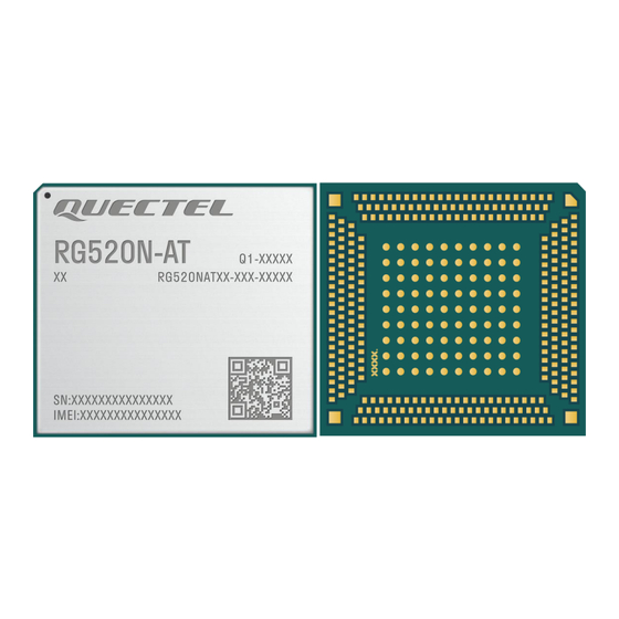
7.3. Top and Bottom Views Figure 51: Top & Bottom Views NOTE Images above are for illustration purpose only and may differ from the actual module. For authentic appearance and label, please refer to the module received from Quectel. RG520N-AT_Hardware_Design 92 / 109... -
Page 94: Storage, Manufacturing & Packaging
5G Module Series Storage, Manufacturing & Packaging 8.1. Storage Conditions The module is provided in vacuum-sealed packaging. MSL of the module is rated at 3. The storage requirements are shown below. 1. Recommended Storage Condition: the temperature should be 23 ± 5 ° C and the relative humidity should be 35–60 %. -
Page 95: Manufacturing And Soldering
5G Module Series NOTE 1. To avoid blistering, layer separation and other soldering issues, extended exposure of the module to the air is forbidden. 2. Take out the module from the package and put it on high-temperature-resistant fixtures before baking. If shorter baking time is desired, see IPC/JEDEC J-STD-033 for the baking procedure. 3. -
Page 96: Packaging Specifications
3. Avoid using ultrasonic technology for module cleaning since it can damage crystals inside the module. 4. Due to the complexity of the SMT process, contact Quectel Technical Support in advance for any situation that you are not sure about, or any process (e.g. selective soldering, ultrasonic soldering) that is not mentioned in document [6]. -
Page 97: Carrier Tape
5G Module Series 8.3.1. Carrier Tape Dimension details are as follow: Figure 53: Carrier Tape Dimension Drawing Table 55: Carrier Tape Dimension Table (Unit: mm) 44.7 41.7 34.2 1.75 8.3.2. Plastic Reel Figure 54: Plastic Reel Dimension Drawing RG520N-AT_Hardware_Design 96 / 109... -
Page 98: Mounting Direction
5G Module Series Table 56: Plastic Reel Dimension Table (Unit: mm) øD1 øD2 72.5 8.3.3. Mounting Direction Figure 55: Mounting Direction RG520N-AT_Hardware_Design 97 / 109... -
Page 99: Packaging Process
5G Module Series 8.3.4. Packaging Process Place the module into the carrier tape and use the cover tape to cover it; then wind the heat-sealed carrier tape to the plastic reel and use the protective tape for protection. 1 plastic reel can load 200 modules. Place the packaged plastic reel, 1 humidity indicator card and 1 desiccant bag into a vacuum bag, vacuumize it. -
Page 100: Appendix A References
5G Module Series Appendix A References Table 57: Related Documents Document Name [1] Quectel_RG520N-AT_CA&EN-DC_Features [2] Quectel_RTA001-EV_EVB_User_Guide [3] Quectel_RG520N&RG52xF&RG530F&RM520N&RM530N_Series_AT_Commands_Manual [4] Quectel_RG520N&RG52xF&RG530F&RM520N&RM530N_Series_GNSS_Application_Note [5] Quectel_RF_Layout_Application_Note [6] Quectel_Module_SMT_Application_Note Table 58: Terms and Abbreviations Abbreviation Description 1PPS 1 Pulse Per Second Analog-to-Digital Converter AMR-WB Adaptive Multi-Rate Wideband Active Optical Network Application Processor BeiDou Navigation Satellite System... - Page 101 5G Module Series Clear To Send CP-OFDM Cyclic Prefix-Orthogonal Frequency Division Multiplexing Digital Audio Interface DC-HSDPA Dual-carrier High Speed Downlink Packet Access Double Data Rate Discrete Fourier Transform-Spread-Orthogonal Frequency Division DFT-s-OFDM Multiplexing Downlink Discontinuous Reception Data Terminal Ready EN-DC E-UTRA New Radio Dual Connectivity Electrostatic Discharge E-UTRA Evolved Universal Terrestrial Radio Access...
- Page 102 5G Module Series Inter-Integrated Circuit Inter-IC Sound Input/Output License Assisted Access Low Band Light Emitting Diode Land Grid Array Low Noise Amplifier Long Term Evolution Media Access Control Middle Band Middle/High Band MIMO Multiple Input Multiple Output Mobile Originated Mobile Terminated New Radio Non-Stand Alone Power Amplifier...
- Page 103 5G Module Series Primary Receive Picosecond Quadrature Amplitude Modulation QPSK Quadrature Phase Shift Keying QZSS Quasi-Zenith Satellite System Radio Frequency RHCP Right Hand Circularly Polarized Receive Stand Alone Sub-Carrier Space Secure Digital System Information Block SIMO Single Input Multiple Output Short Message Service System on a Chip Serial Peripheral Interface...
- Page 104 5G Module Series Unsolicited Result Code Universal Serial Bus (U)SIM Universal Subscriber Identity Module VBAT Voltage at Battery (Pin) Vmax Maximum Voltage Vmin Minimum Voltage Vnom Nominal Voltage VSWR Voltage Standing Wave Ratio WLAN Wireless Local Area Network WWAN Wireless Wide Area Network RG520N-AT_Hardware_Design 103 / 109...
-
Page 105: Appendix B Operating Frequencies
5G Module Series Appendix B Operating Frequencies Table 59: Operating Frequencies (5G) Duplex Uplink Operating Downlink Operating Unit Mode Frequency Frequency 1920–1980 2110–2170 1850–1910 1930–1990 1710–1785 1805–1880 824–849 869–894 2500–2570 2620–2690 880–915 925–960 699–716 729–746 777–787 746–756 788–798 758–768 815–830 860–875 832–862 791–821... - Page 106 5G Module Series 1880–1920 1880–1920 2300–2400 2300–2400 2496–2690 2496–2690 5150–5925 5150–5925 5855–5925 5855–5925 3550–3700 3550–3700 1432–1517 1432–1517 1427–1432 1427–1432 2483.5–2495 2483.5–2495 1920–2010 2110–2200 1710–1780 2110–2200 738–758 1695–1710 1995–2020 663–698 617–652 1427–1470 1475–1518 1432–1517 1427–1432 3300–4200 3300–4200 3300–3800 3300–3800 4400–5000 4400–5000 1710–1785 880–915 832–862...
- Page 107 5G Module Series 1710–1780 824–849 2496–2690 2496–2690 832–862 1427–1432 832–862 1432–1517 880–915 1427–1432 880–915 1432–1517 2010–2025 5925–7125 5925–7125 2300–2400 1880–1920 1626.5–1660.5 n257 26.50–29.50 26.50–29.50 n258 24.25–27.50 24.25–27.50 n260 37.00–40.00 37.00–40.00 n261 27.50–28.35 27.50–28.35 Table 60: Operating Frequencies (2G + 3G + 4G) Uplink Downlink Duplex Mode...
- Page 108 5G Module Series 2500–2570 2620–2690 EGSM900 880–915 925–960 1749.9–1784.9 1844.9–1879.9 1710–1770 2110–2170 1427.9–1447.9 1475.9–1495.9 699–716 729–746 777–787 746–756 788–798 758–768 704–716 734–746 815–830 860–875 830–845 875–890 832–862 791–821 1447.9–1462.9 1495.9–1510.9 3410–3490 3510–3590 1626.5–1660.5 1525–1559 1850–1915 1930–1995 814–849 859–894 807–824 852–869 703–748 758–803 717–728...
- Page 109 5G Module Series 1850–1910 1850–1910 1930–1990 1930–1990 1910–1930 1910–1930 2570–2620 2570–2620 1880–1920 1880–1920 2300–2400 2300–2400 2496–2690 2496–2690 3400–3600 3400–3600 3600–3800 3600–3800 703–803 703–803 1447–1467 1447–1467 5150–5925 5150–5925 5855–5925 5855–5925 3550–3700 3550–3700 1432–1517 1432–1517 1427–1432 1427–1432 3300–3400 3300–3400 1920–2010 2110–2200 1710–1780 2110–2200 738–758 698–728...
- Page 110 5G Module Series 451–456 461–466 450–455 460–465 1427–1470 1475–1518 1432–1517 1427–1432 698–716 728–746 410–415 420–425 412–417 422–427 RG520N-AT_Hardware_Design 109 / 109...
- Page 111 Quectel that they wish to change the antenna trace design. In this case, a Class II permissive change application is required to be filed by...
- Page 112 Antenna (1) The antenna must be installed such that 20 cm is maintained between the antenna and users, (2) The transmitter module may not be co-located with any other transmitter or antenna. In the event that these conditions cannot be met (for example certain laptop configurations or co-location with another transmitter), then the FCC authorization is no longer considered valid and the FCC ID cannot be used on the final product.
- Page 113 Federal Communication Commission Interference Statement This device complies with Part 15 of the FCC Rules. Operation is subject to the following two conditions: (1) This device may not cause harmful interference, and (2) this device must accept any interference received, including interference that may cause undesired operation. This equipment has been tested and found to comply with the limits for a Class B digital device, pursuant to Part 15 of the FCC Rules.
- Page 114 This device is intended only for OEM integrators under the following conditions: (For module device use) 1) The antenna must be installed such that 20 cm is maintained between the antenna and users, and 2) The transmitter module may not be co-located with any other transmitter or antenna. As long as 2 conditions above are met, further transmitter test will not be required.
Need help?
Do you have a question about the RG520N-AT and is the answer not in the manual?
Questions and answers