
Related Manuals for Quectel RG255C-GL


Summary of Contents for Quectel RG255C-GL
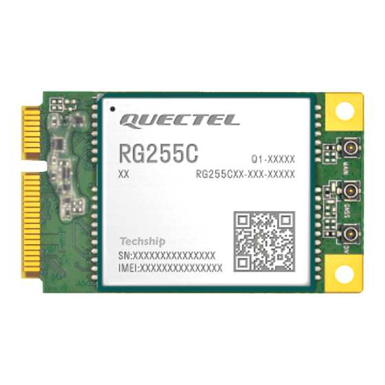
- Page 1 RG255C-GL Mini PCIe Hardware Design 5G Module Series Version: 1.0.0 Date: 2023-08-25 Status: Preliminary...
- Page 2 5G Module Series At Quectel, our aim is to provide timely and comprehensive services to our customers. If you require any assistance, please contact our headquarters: Quectel Wireless Solutions Co., Ltd. Building 5, Shanghai Business Park Phase III (Area B), No.1016 Tianlin Road, Minhang District, Shanghai...
- Page 3 Except as otherwise set forth herein, nothing in this document shall be construed as conferring any rights to use any trademark, trade name or name, abbreviation, or counterfeit product thereof owned by Quectel or any third party in advertising, publicity, or other aspects.
-
Page 4: Safety Information
Manufacturers of the terminal should notify users and operating personnel of the following safety information by incorporating these guidelines into all manuals of the product. Otherwise, Quectel assumes no liability for customers’ failure to comply with these precautions. -
Page 5: About The Document
5G Module Series About the Document Revision History Version Date Author Description Mike CHEN/ 2023-08-25 Ethan FANG/ Creation of the document Sherlock ZHAO Mike CHEN/ 1.0.0 2023-08-25 Ethan FANG/ Preliminary Sherlock ZHAO RG255C-GL_Mini_PCIe_Hardware_Design 4 / 57... -
Page 6: Table Of Contents
5G Module Series Contents Safety Information ............................. 3 About the Document ..........................4 Contents ..............................5 Table Index ..............................7 Figure Index ............................... 8 Introduction ............................9 1.1. Special Mark ..........................9 Product Overview ..........................10 2.1. Frequency Bands and Functions ................... 10 2.2. - Page 7 5G Module Series 5.2.3.1. GNSS Frequency ....................38 5.2.3.2. GNSS Performance ................... 38 5.3. Recommended Mating Plugs for Antenna Connection ............39 3.1.1 Recommended RF Connector for Installation ............. 41 5.3.1.1. Assemble Coaxial Cable Plug Manually ............41 5.3.1.2. Assemble Coaxial Cable Plug with Jig .............. 42 3.1.2 Recommended Manufacturers of RF Connector and Cable ........
- Page 8 5G Module Series Table Index Table 1: Special Mark ..........................9 Table 2: Frequency Bands and Functions ....................10 Table 3: Key Features ..........................11 Table 4: Parameter Definition ........................14 Table 5: Pin Description ..........................15 Table 6: Overview of Operating Modes ..................... 19 Table 7: Definition of VCC_3V3 and GND Pins ..................
- Page 9 5G Module Series Figure Index Figure 1: Functional Diagram ........................13 Figure 2: Pin Assignment .......................... 14 Figure 3: Module Power Consumption in Sleep Mode ................20 Figure 4: Reference Circuit of Power Supply .................... 21 Figure 5: Reference Circuit of (U)SIM Interface with an 8-pin (U)SIM Card Connector ......23 Figure 6: Reference Circuit of (U)SIM Interface with a 6-pin (U)SIM Card Connector ......
-
Page 10: Introduction
5G Module Series Introduction This document defines RG255C-GL Mini PCIe module, and describes its air interfaces and hardware interfaces which are connected with your applications. With this document, you can quickly understand module interface specifications, electrical and mechanical details, as well as other related information of the module. The document, coupled with application notes and user guides, makes it easy to design and set up wireless applications with the module. -
Page 11: Product Overview
Product Overview 2.1. Frequency Bands and Functions RG255C-GL Mini PCIe module provides data connectivity on 5G NR SA, LTE-FDD, LTE-TDD networks with PCI Express Mini Card 1.2 standard interface. It supports embedded operating systems, such as Linux and Android, and provides audio, high-speed data transmission, and GNSS functionalities (optional) to meet your specific application demands. -
Page 12: Key Features
5G NR FDD bands only support 15 kHz SCS, and NR TDD bands only support 30 kHz SCS. The maximum rates are theoretical and the actual values depend on the network configuration. If you need the function of L2, contact Quectel Technical Support. RG255C-GL_Mini_PCIe_Hardware_Design... - Page 13 5G Module Series ⚫ Compliant with 3GPP TS 27.007, 3GPP TS 27.005 AT Commands ⚫ Quectel enhanced AT commands Supports TCP/UDP/SSL*/TLS*/FTP(S)*/HTTP(S)*/MQTT(S)*/SMTP(S)*/ Internet Protocol Features NTP*/PING/NITZ*/LwM2M* protocols USB Tethering RmNet, RNDIS, ECM, DUN, MBIM ⚫ Only Support SGS, IMS and NAS SMS ⚫...
-
Page 14: Functional Diagram
5G Module Series RoHS All hardware components are fully compliant with EU RoHS directive 2.3. Functional Diagram The following figure shows the block diagram of the module. VCC_3V3 VBAT Boost Circuit Main Main Antenna Antenna Connector PCM&I2C GNSS GNSS Antenna RG255C Module UART Antenna... -
Page 15: Pin Assignment
5G Module Series 2.4. Pin Assignment The following figure shows the pin assignment of the module. The top side contains RG255C-GL module and antenna connectors. Pin Name Pin Name Pin No. Pin No. WAKE# VCC_3V3 RESERVED RESERVED RESERVED USIM_VDD PIN1... - Page 16 5G Module Series Open Collector Power Input Power Output DC characteristics include power domain and rate current. Table 5: Pin Description Pin No. Pin Name Description Comment Characteristics WAKE# Wake up the host Vmin = 3.0 V Power supply for the VCC_3V3 Vnom = 3.3 V module...
- Page 17 5G Module Series USIM_RST (U)SIM card reset USIM_VDD Ground RESERVED Reserved Ring indication 3.3 V Ground RESERVED Reserved Pulled up by W_DISABLE# Airplane mode control 3.3 V default. Active low. Ground Pulled up by PERST# Fundamental reset 3.3 V default. Active low.
- Page 18 5G Module Series Requires differential impedance of USB 2.0 differential data 90 Ω. USB_DM A Test point must be reserved. Ground Requires differential impedance of USB 2.0 differential data 90 Ω. USB_DP A Test point must be reserved. Vmin = 3.0 V Power supply for the VCC_3V3 Vnom = 3.3 V...
-
Page 19: Evb Kit
Vmax = 3.6 V NOTE Keep all NC, RESERVED and unused pins unconnected. 2.6. EVB Kit Quectel supplies an evaluation board (Mini PCIe EVB) with accessories to develop and test the module. For more details, see documents [2]. RG255C-GL_Mini_PCIe_Hardware_Design 18 / 57... -
Page 20: Operating Characteristics
5G Module Series Operating Characteristics 3.1. Operating Modes The following table briefly outlines the operating modes to be mentioned in the following chapters. Table 6: Overview of Operating Modes Mode Details The module remains registered on the network, and is ready to send Idle and receive data. -
Page 21: Sleep Mode
5G Module Series 3.2. Sleep Mode RG255C-GL Mini PCIe is able to reduce its power consumption to an ultra-low level in sleep mode. There are three preconditions must be met to make the module enter sleep mode. ⚫ Execute AT+QSCLK=1 to enable sleep mode. -
Page 22: Power Supply
4, 9, 15, 18, 21, 26, 27, 29, 34, 35, 37, 40, 43, 50 The typical supply voltage of RG255C-GL Mini PCIe is 3.3 V. The power supply must be able to provide a rated output current of 3.5 A at least, and a bypass capacitor of not less than 470 µF with low ESR should be used to prevent the voltage from dropping. -
Page 23: Application Interfaces
5G Module Series Application Interfaces The physical connections and signal levels of RG255C-GL Mini PCIe comply with PCI Express Mini Card Electromechanical Specification. This chapter mainly describes the definition and application of the following interfaces and pins of RG255C-GL Mini PCIe: ⚫... - Page 24 5G Module Series USIM_VDD 100 nF Module (U)SIM Card Connector USIM_VDD USIM_VDD USIM_RST USIM_CLK USIM_DET USIM_DATA 33 pF 33 pF 33 pF Figure 5: Reference Circuit of (U)SIM Interface with an 8-pin (U)SIM Card Connector If (U)SIM card hot-plug detect is not needed, keep USIM_DET unconnected. A reference circuit for (U)SIM interface with a 6-pin (U)SIM card connector is illustrated in the following figure.
-
Page 25: Usb Interface
(U)SIM card connector. 4.2. USB Interface RG255C-GL Mini PCIe provides one integrated Universal Serial Bus (USB) interface which complies with USB 2.0 specification. It can only be used as a slave device. Meanwhile, it supports high-speed (480 Mbps) mode and full-speed (12 Mbps) mode. -
Page 26: Uart
Keep the ESD protection components as close to the USB connector as possible. 4.3. UART RG255C-GL Mini PCIe provides one main UART that supports 115200 bps, 9600 bps, 19200 bps, 38400 bps, 57600 bps, and 230400 bps baud rates, and the default is 115200 bps. It supports RTS and CTS hardware flow control, and can be used for AT command communication and data transmission. -
Page 27: Pcm* And I2C Interfaces
AT+IPR can be used to set the baud rate of the main UART, and AT+IFC can be used to set the hardware flow control (hardware flow control is disabled by default). See document [3] for details. 4.4. PCM* and I2C Interfaces RG255C-GL Mini PCIe provides one Pulse Code Modulation (PCM) digital interface and one I2C interface. RG255C-GL_Mini_PCIe_Hardware_Design 26 / 57... - Page 28 5G Module Series The following table shows the pin definition of PCM and I2C interfaces that can be applied in audio codec design. Table 11: Pin Definition of PCM and I2C Interfaces Pin Name Pin No. Description Comment PCM_CLK PCM clock PCM_DOUT PCM data output 1.8 V power domain.
- Page 29 (master mode, PCM_CLK = 2048 kHz, PCM_SYNC = 8 kHz, 16-bit linear data format). In addition, RG255C-GL Mini PCIe’s firmware has integrated the configuration on some PCM codec’s application with I2C interface. See document [3] for details about AT+QDAI.
-
Page 30: Control And Indication Signals
5G Module Series NOTE It is recommended to reserve an RC (R = 0 Ω, C = 33 pF) circuit on the PCM lines, especially for PCM_CLK. The module can only be used as a master device in applications related to PCM and I2C interfaces 4.5. -
Page 31: W_Disable
5G Module Series 4.5.1. RI The RI signal can be used to wake up the host. When a URC returns, there will be the following behaviors on the RI pin after executing AT+QCFG="risignaltype","physical". Figure 12: RI Behaviors 4.5.2. W_DISABLE# The module provides a W_DISABLE# signal to disable or enable the RF function (excluding GNSS). The W_DISABLE# pin is pulled up by default. -
Page 32: Dtr
5G Module Series NOTE The execution of AT+CFUN does not affect GNSS function. 4.5.3. DTR The DTR signal is used for sleep mode control. It is pulled up by default. When the module is in sleep mode, driving DTR low can wake up the module. For more details about the preconditions for the module to enter sleep mode, see Chapter 3.2. -
Page 33: Wake
5G Module Series Figure 14: LED_WWAN# Signal Reference Circuit Diagram There are two indication modes for LED_WWAN# signal to indicate network status, which can be switched through following AT commands: ⚫ AT+QCFG="ledmode",0 (default setting) ⚫ AT+QCFG="ledmode",2 The following tables show the detailed network status indications of the LED_WWAN# signal. Table 15: Indications of Network Status (AT+QCFG="ledmode",0, Default Setting) Pin Status Description... - Page 34 5G Module Series Figure 15: WAKE# Behaviors RG255C-GL_Mini_PCIe_Hardware_Design 33 / 57...
-
Page 35: Antenna Connection
Antenna Connection 5.1. Antenna Connectors RG255C-GL Mini PCIe is mounted with three antenna connectors for external antenna connection: a main antenna connector, an Rx-diversity antenna connector, and a GNSS antenna connector. And Rx-diversity function is enabled by default. The impedance of the antenna connectors is 50 Ω. -
Page 36: Cellular Network
5G Module Series 5.2.2. Cellular Network 5.2.2.1. Rx Sensitivity Table 18: Conducted RF Receiving Sensitivity (Unit: dBm) Receiving Sensitivity (Typ.) Mode Frequency Bands 3GPP (SIMO) Primary Diversity SIMO LTE-FDD B1 (10 MHz) LTE-FDD B2 (10 MHz) LTE-FDD B3 (10 MHz) LTE-FDD B4 (10 MHz) LTE-FDD B5 (10 MHz) LTE-FDD B7 (10 MHz) - Page 37 5G Module Series LTE-TDD B34 (10 MHz) LTE-TDD B38 (10 MHz) LTE-TDD B39 (10 MHz) LTE-TDD B40 (10 MHz) LTE-TDD B41 (10 MHz) LTE-TDD B42 (10 MHz) LTE-TDD B43 (10 MHz) LTE-TDD B48 (10 MHz) LTE-FDD B66 (10 MHz) LTE-FDD B70* (10 MHz) LTE-FDD B71 (10 MHz)
-
Page 38: Tx Power
5G Module Series 5G NR FDD n30 (10 MHz) 5G NR TDD n38 (20 MHz) 5G NR TDD n40 (20 MHz) 5G NR TDD n41 (20 MHz) 5G NR FDD n48 (20 MHz) 5G NR FDD n66 (20 MHz) 5G NR FDD n70* (20 MHz) 5G NR FDD n71 (20 MHz) -
Page 39: Gnss (Optional)
1176.45 ± 10.23 (E5a) 5.2.3.2. GNSS Performance The following table shows GNSS performance of the module. Table 21: GNSS Performance Parameter Description Conditions Typ. Unit Acquisition Sensitivity Reacquisition Autonomous Tracking If you need this function, contact Quectel Technical Support. RG255C-GL_Mini_PCIe_Hardware_Design 38 / 57... -
Page 40: Recommended Mating Plugs For Antenna Connection
3 minutes continuously). 5.3. Recommended Mating Plugs for Antenna Connection RG255C-GL Mini PCIe is mounted with RF connectors (receptacles) for convenient antenna connection. The dimensions of the antenna connectors are shown as below. Figure 16: Dimensions of the Receptacle RF Connectors (Unit: mm) - Page 41 5G Module Series U.FL-LP mating plugs listed in the following figure can be used to match the receptacles. Figure 17: Mechanicals of U.FL-LP Mating Plugs The following figure describes the space factor of mating plugs. Figure 18: Space Factor of Mating Plugs (Unit: mm) RG255C-GL_Mini_PCIe_Hardware_Design 40 / 57...
-
Page 42: Recommended Rf Connector For Installation
5G Module Series 5.3.1. Recommended RF Connector for Installation 5.3.1.1. Assemble Coaxial Cable Plug Manually The illustration for plugging in a coaxial cable plug is shown below, θ = 90° is acceptable, while θ ≠ 90° is not. Figure 41: Plug in a Coaxial Cable Plug The illustration of pulling out the coaxial cable plug is shown below, θ... -
Page 43: Assemble Coaxial Cable Plug With Jig
5G Module Series 5.3.1.2. Assemble Coaxial Cable Plug with Jig The pictures of installing the coaxial cable plug with a jig is shown below, θ = 90° is acceptable, while θ ≠ 90° is not. Figure 43: Install the Coaxial Cable Plug with Jig 5.3.2. -
Page 44: Electrical Characteristics And Reliability
⚫ Thermal dissipation 6.1. Power Supply Requirements The input voltage of RG255C-GL Mini PCIe is 3.0–3.6 V, as specified by PCI Express Mini Card Electromechanical Specification Revision 1.2. The following table shows the power supply requirements of RG255C-GL Mini PCIe. -
Page 45: Digital I/O Characteristic
5G Module Series 6.2. Digital I/O Characteristic The following table shows the I/O requirements of RG255C-GL Mini PCIe. Table 23: I/O Requirements Parameter Description Min. Max. Unit High-level input voltage 0.7 × VCC_3V3 VCC_3V3 + 0.3 Low-level input voltage -0.3 0.3 ×... -
Page 46: Power Consumption
5G Module Series Table 25: Electrostatic Discharge Characteristics (Temperature: 25–30 ° C, Humidity: 40 ± 5 %) Tested Interfaces Contact Discharge Air Discharge Unit VBAT, GND ± 5 ± 10 Antenna Interfaces ± 4 ± 8 Other Interfaces ± 0.5 ±... -
Page 47: Thermal Dissipation
5G Module Series Table 27: GNSS Power Consumption Description Condition Typ. Unit Cold start @ Passive antenna Searching (AT+CFUN=0) Lost state @ Passive antenna Tracking Instrument environment (AT+CFUN=0) 6.5. Thermal Dissipation Figure 19: Distribution of Heat Source Chips Inside the Module The module offers the best performance when all internal IC chips are working within their operating temperatures. - Page 48 5G Module Series still work but the performance and function (such as RF output power, data rate) will be affected to a certain extent. Therefore, the thermal design should be maximally optimized to ensure all internal IC chips always work within the recommended operating temperature range. The following principles for thermal consideration are provided for reference: ⚫...
-
Page 49: Notification
5G Module Series reduced performance (such as RF output power, data rate). When the maximum BB chip temperature reaches or exceeds 105 ° C, the module will disconnect from the network, and it will recover to network connected state after the maximum temperature falls below 105 ° C. Therefore, the thermal design should be maximally optimized to make sure the maximum BB chip temperature always maintains below 95 °... -
Page 50: Mechanical Information
5G Module Series Mechanical Information This chapter mainly describes mechanical dimensions as well as packaging specification of RG255C-GL Mini PCIe module. All dimensions are measured in millimeter (mm), and the dimensional tolerances are ± 0.15 mm unless otherwise specified. 7.1. Mechanical Dimensions... -
Page 51: Standard Dimensions Of Mini Pci Express
5G Module Series 7.2. Standard Dimensions of Mini PCI Express RG255C-GL Mini PCIe adopts a standard Mini PCI Express connector which compiles with the directives and standards listed in the PCI Express Mini Card Electromechanical Specification Revision 1.2. The following figure takes the Molex 679105700 as an example. -
Page 52: Top And Bottom Views
5G Module Series 7.2. Top and Bottom Views Figure 23: Top and Bottom Views of the Module Figure 24: Test Points of the Module RG255C-GL_Mini_PCIe_Hardware_Design 51 / 57... -
Page 53: Packaging Specifications
5G Module Series 7.3. Packaging Specifications This chapter describes only the key parameters and process of packaging. All figures below are for reference only. The appearance and structure of the packaging materials are subject to the actual delivery. The module adopts blister tray packaging and details are as follow: 7.3.1. -
Page 54: Packaging Process
5G Module Series 7.3.2. Packaging Process Each blister tray packs 10 modules. Stack 10 Packing 11 blister trays together and then put blister trays with modules together, and put 1 blister trays into conductive bag, seal and empty blister tray on the top. pack the conductive bag. -
Page 55: Appendix References
5G Module Series Appendix References Table 28: Related Documents Document Name [1] Quectel_RG255C-GL_Hardware_Design [2] Quectel_Mini_PCIe_EVB_User_Guide [3] Quectel_RG255C_Series&RM255C-GL_AT_Commands_Manual Table 29: Terms and Abbreviations Abbreviation Description Adaptive Multi-rate BeiDou Navigation Satellite System Bits Per Second CMUX Connection Multiplexing Coding Scheme Clear to Send DFOTA Delta Firmware Upgrade Over-The-Air Downlink... - Page 56 5G Module Series Electrostatic Discharge Equivalent Series Resistance Frequency Division Duplexing Full Rate File Transfer Protocol FTPS FTP over SSL GLONASS Russian Global Navigation Satellite System GNSS Global Navigation Satellite System Global Positioning System Half Rate HTTP Hypertext Transfer Protocol HTTPS Hypertext Transfer Protocol Secure IP Multimedia Subsystem...
- Page 57 5G Module Series NDIS Network Driver Interface Specification NMEA National Marine Electronics Association Network Time Protocol Power amplifier Pulse Code Modulation Personal Digital Assistant Protocol Data Unit PING Packet Internet Groper Point of Sale Quadrature Amplitude Modulation QPSK Quadrature Phase Shift Keying Radio Frequency RmNet Remote Network...
- Page 58 5G Module Series Transmitting Direction Transient Voltage Suppressor UART Universal Asynchronous Receiver & Transmitter User Datagram Protocol Uplink Unsolicited Result Code Universal Serial Bus (U)SIM (Universal) Subscriber Identification Module WLAN Wireless Local Area Network RG255C-GL_Mini_PCIe_Hardware_Design 57 / 57...
Need help?
Do you have a question about the RG255C-GL and is the answer not in the manual?
Questions and answers