
Related Manuals for Quectel RM502Q-GL


Summary of Contents for Quectel RM502Q-GL
- Page 1 RM502Q-GL Hardware Design 5G Module Series Rev. RM502Q-GL_Hardware_Design_V1.0 Date: 2020-07-06 Status: Preliminary www.quectel.com...
- Page 2 QUECTEL OFFERS THE INFORMATION AS A SERVICE TO ITS CUSTOMERS. THE INFORMATION PROVIDED IS BASED UPON CUSTOMERS’ REQUIREMENTS. QUECTEL MAKES EVERY EFFORT TO ENSURE THE QUALITY OF THE INFORMATION IT MAKES AVAILABLE. QUECTEL DOES NOT MAKE ANY WARRANTY AS TO THE INFORMATION CONTAINED HEREIN, AND DOES NOT ACCEPT ANY LIABILITY FOR ANY INJURY, LOSS OR DAMAGE OF ANY KIND INCURRED BY USE OF OR RELIANCE UPON THE INFORMATION.
-
Page 3: About The Document
5G Module Series RM502Q-GL Hardware Design About the Document Revision History Version Date Author Description Kingson ZHANG/ 2020-07-06 Initial Qiqi WANG RM502Q-GL_Hardware_Design 2 / 77... -
Page 4: Table Of Contents
5G Module Series RM502Q-GL Hardware Design Contents About the Document ........................... 2 Contents ............................... 3 Table Index ..............................5 Figure Index ..............................6 Introduction ............................8 1.1. Safety Information ........................9 Product Concept ..........................10 2.1. General Description ........................10 2.2. - Page 5 5G Module Series RM502Q-GL Hardware Design 3.12. Antenna Tuner Control Interface* ..................... 45 3.13. Configuration Pins ........................46 GNSS Receiver ........................... 47 4.1. General Description ........................47 4.2. GNSS Performance ........................48 Antenna Connection .......................... 49 5.1. RF Antenna Interfaces ......................49 5.1.1.
- Page 6 5G Module Series RM502Q-GL Hardware Design Table Index Table 1: Frequency Bands and GNSS Type of RM502Q-GL Module ............10 Table 2: Key Features of RM502Q-GL ...................... 11 Table 3: Definition of I/O Parameters ......................17 Table 4: Pin Description ..........................17 Table 5: Definition of VCC and GND Pins ....................
- Page 7 Figure 34: Coplanar Waveguide Design on a 4-layer PCB (Layer 4 as Reference Ground) ....55 Figure 35: Antenna Connectors on the Module ..................56 Figure 36: RM502Q-GL RF Connector Dimensions (Unit: mm) ..............58 Figure 37: Specifications of Mating Plugs Using Ø0.81 mm Coaxial Cables ..........58 Figure 38: Connection between RF Connector and Mating Plug Using Ø0.81 mm Coaxial Cable ..
- Page 8 5G Module Series RM502Q-GL Hardware Design Figure 42: Top and Bottom Views of the Module ..................74 Figure 43: Tray Size (Unit: mm) ......................... 75 Figure 44: Tray Packaging Procedure ....................... 75 RM502Q-GL_Hardware_Design 7 / 77...
-
Page 9: Introduction
This document helps customers quickly understand the interface specifications, electrical and mechanical details, as well as other related information of RM502Q-GL module. To facilitate its application in different fields, reference design is also provided for reference. Associated with application notes and user guides, customers can use the module to design and set up mobile applications easily. -
Page 10: Safety Information
The following safety precautions must be observed during all phases of operation, such as usage, service or repair of any cellular terminal or mobile incorporating RM502Q-GL module. Manufacturers of the cellular terminal should notify users and operating personnel of the following safety information by incorporating these guidelines into all manuals of the product. -
Page 11: Product Concept
It supports embedded operating systems such as Windows, Linux and Android, and also provides GNSS and voice functionality to meet specific application demands. The following table shows the frequency bands and GNSS type of RM502Q-GL module. Table 1: Frequency Bands and GNSS Type of RM502Q-GL Module... -
Page 12: Key Features
5G Module Series RM502Q-GL Hardware Design RM502Q-GL can be applied in the following fields: ⚫ Rugged tablet PC and laptop computer ⚫ Remote monitor system ⚫ Vehicle system ⚫ Wireless POS system ⚫ Smart metering system ⚫ Wireless router and switch ⚫... - Page 13 Rx-diversity Support 5G NR/LTE/WCDMA Rx-diversity Gen9 Lite of Qualcomm GNSS Features Protocol: NMEA 0183 Data Update Rate: 1 Hz Compliant with 3GPP TS 27.007, 27.005 and Quectel enhanced AT AT Commands commands Antenna Interfaces ANT0, ANT1, ANT2_GNSSL1, and ANT3 Physical Size: (52.0 ±...
-
Page 14: Functional Diagram
3GPP. When the temperature returns to the normal operating temperature level, the module will meet 3GPP specifications again. “*” means under development. 2.3. Functional Diagram The following figure shows a block diagram of RM502Q-GL. PMIC FULL_CARD_POWER_OFF# RESET_N 38.4M... -
Page 15: Evaluation Board
RM502Q-GL Hardware Design 2.4. Evaluation Board To help with the development of applications conveniently with RM502Q-GL, Quectel supplies the evaluation board (PCIe Card EVB), a USB to RS-232 converter cable, a USB type-C cable, antennas and other peripherals to control or test the module. For more details, please refer to document [1]. -
Page 16: Application Interfaces
5G Module Series RM502Q-GL Hardware Design Application Interfaces The physical connections and signal levels of RM502Q-GL comply with PCI Express M.2 specification. This chapter mainly describes the definition and application of the following interfaces/pins of RM502Q-GL: ⚫ Power supply ⚫... -
Page 17: Pin Assignment
5G Module Series RM502Q-GL Hardware Design 3.1. Pin Assignment The following figure shows the pin assignment of RM502Q-GL. The top side contains RM502Q-GL module and antenna connectors. Pin Name Pin Name CONFIG_2 CONFIG_1 AP2SDX_STATUS RESET_N USIM1_DET RFFE_VIO_1V8 COEX_TXD RFFE0_CLK COEX_RXD... -
Page 18: Pin Description
Analog Input Analog Output Digital Input Digital Output Bidirectional Open Drain Power Input Power Output The following table shows the pin definition and description of RM502Q-GL. Table 4: Pin Description M.2 Socket 2 RM502Q-GL PCIe-based Description Comment Pin Name Pinout... - Page 19 5G Module Series RM502Q-GL Hardware Design 100k Ω resistor (I)(0/1.8 V) module is turned off. When it is at high level, the module is turned on. USB_D+ USB_DP USB 2.0 differential data (+) W_DISABLE1# Airplane mode control. 1.8/3.3 V power W_DISABLE1# (I)(0/1.8 V)
- Page 20 5G Module Series RM502Q-GL Hardware Design GPIO_8 1.8 V power PCM_SYNC PCM data frame sync /AUDIO_3 domain PETn1 USB_SS_TX_M USB 3.1 transmit data (-) 1.8/3.0 V power UIM_RESET(O) USIM1_RST (U)SIM1 card reset domain PETp1 USB_SS_TX_P USB 3.1 transmit data (+) 1.8/3.0 V power...
- Page 21 5G Module Series RM502Q-GL Hardware Design Ground PCIe clock request. CLKREQ# PCIE_CLKREQ_N Open drain Active LOW. REFCLKn PCIE_REFCLK_M PCIe reference clock (-) PCIe PME wake. PEWAKE# PCIE_WAKE_N Open drain Active LOW. REFCLKp PCIE_REFCLK_P PCIe reference clock (+) 1.8 V power...
-
Page 22: Power Supply
5G Module Series RM502Q-GL Hardware Design Ground Vmin = 3.135 V 3.3 V Power supply Vnorm = 3.7 V Vmax = 4.4 V Ground Vmin = 3.135 V 3.3 V Power supply Vnorm = 3.7 V Vmax = 4.4 V... -
Page 23: Reference Design For Power Supply
5G Module Series RM502Q-GL Hardware Design Voltage Ripple Voltage Drop < 100mV Figure 3: Power Supply Limits during Radio Transmission The main power supply from an external system must be a single voltage source. To decrease voltage drop, a bypass capacitor of about 100 µF with low ESR (ESR = 0.7 Ω) should be used, and a multi-layer ceramic chip capacitor (MLCC) array also should be used due to its ultra-low ESR. -
Page 24: Turn On And Off Scenarios
5G Module Series RM502Q-GL Hardware Design The following figure shows a reference design for +5 V input power source based on an DC-DC TPS54319. The typical output of the power supply is about 3.7 V and the maximum load current is 3 A. -
Page 25: Turn On The Module With A Host Gpio
5G Module Series RM502Q-GL Hardware Design When it is at high level, the module is powered on. 3.4.1.1. Turn on the Module with a Host GPIO It is recommended to use a host GPIO to control FULL_CARD_POWER_OFF#. A simple reference circuit is illustrated in the following figure. -
Page 26: Turn On The Module With Compatible Design
5G Module Series RM502Q-GL Hardware Design 3.4.1.3. Turn on the Module with Compatible Design The following figure shows a compatible design to turn on the module automatically after power-up or by host. Auto turn on Turn on by host Host Module 0Ω... -
Page 27: Turn Off The Module
5G Module Series RM502Q-GL Hardware Design internal LDO output) HIGH level, which is typically 68 ms. is the time interval between VCC and FULL_CARD_POWER_OFF# HIGH level. It could be 0 by turning on the module automatically as shown in Figure 7, or any other time decided by the host as shown in Figure 6. - Page 28 5G Module Series RM502Q-GL Hardware Design RESET_N(H) USB/PCIe AT+QPOWD removed USB/PCIe FULL_CARD_POWER_OFF# Module Status RUNNING Turn off procedure Figure 11: Turn-off Timing through AT Command and FULL_CARD_POWER_OFF# For the circuit design of Figure 7, please cut off power supply of VCC after the module USB/PCIe is removed, as illustrated in Figure 11.
-
Page 29: Reset
5G Module Series RM502Q-GL Hardware Design 3.5. Reset RESET_N is an asynchronous and active low signal (1.8 V logic level). Whenever this pin is active, the modem will immediately be placed in a Power On Reset(POR) condition. CAUTION: Triggering the RESET# signal will lead to loss of all data in the modem and the removal of system drivers. - Page 30 5G Module Series RM502Q-GL Hardware Design Host Module VDD 1.8V 100k RESET_N Reset pulse Reset Logic GPIO NMOS 200-700 ms 100k Figure 14: Reference Circuit of RESET_N with NMOS Driving Circuit VDD 1.8V 100k RESET_N Reset Logic 33pF 200-700ms Note: The capacitor C1 is recommended to be less than 47pF.
-
Page 31: U)Sim Interfaces
NOTE “*” means under development. RM502Q-GL supports (U)SIM card hot-plug via the USIM_DET pin, which is a level trigger pin. With a normally closed (U)SIM card connector, the USIM_DET is normally short-circuited to ground when a (U)SIM card is not inserted, and the USIM_DET will change from low to high level when the (U)SIM card is inserted. - Page 32 5G Module Series RM502Q-GL Hardware Design USIM1_VDD Module (U)SIM Card Connector 100 nF 10-20k USIM1_VDD USIM1_RST USIM1_CLK USIM1_DET USIM1_DATA Note: All these resistors, capacitors and TVS should be close to (U)SIM card connector in PCB layout. Figure 17: Reference Circuit of Normally Closed (U)SIM Card Connector Normally Closed (U)SIM Card Connector: ⚫...
-
Page 33: Usb Interface
(U)SIM card connector. 3.7. USB Interface RM502Q-GL provides one integrated Universal Serial Bus (USB) interface which complies with the USB 3.1 & 2.0 specifications and supports super speed (10) on USB 3.1 and high speed (480 Mbps) and full speed (12 Mbps) modes on USB 2.0. - Page 34 5G Module Series RM502Q-GL Hardware Design Please note that only USB 2.0 can be used for firmware upgrade currently. The following table shows the pin definition of USB interface. Table 9: Pin Definition of USB Interface Pin No. Pin Name...
- Page 35 5G Module Series RM502Q-GL Hardware Design AC coupling capacitors C5 and C6 must be placed close to the host and close to each other. C1 and C2 have been integrated inside the module, so do not place these two capacitors on customers’ schematic and PCB.
-
Page 36: Pcie Interface
PCIE_WAKE_N Open drain Active LOW. 3.8.1. Endpoint Mode RM502Q-GL supports endpoint (EP) mode. In this mode, the module is configured as a PCIe EP device. The following figure shows a reference circuit of PCIe EP mode. RM502Q-GL_Hardware_Design 35 / 77... - Page 37 5G Module Series RM502Q-GL Hardware Design Host Module PCIE_REFCLK_P PCIE_REFCLK_P PCIE_REFCLK_M PCIE_REFCLK_M PCIE_RX_P C5 220nF PCIE_TX_P PCIE_RX_M C6 220nF PCIE_TX_M PCIE_TX_P C1 220nF PCIE_RX_P PCIE_TX_M C2 220nF PCIE_RX_M PCIE_WAKE_N PCIE_WAKE_N PCIE_CLKREQ_N PCIE_CLKREQ_N PCIE_RST_N PCIE_RST_N 100k 100k 100k VCC_IO_HOST Note: The voltage level of VCC_IO_HOST depends on the host side due to the open drain in pins 50, 52 and 54.
-
Page 38: Usb Version And Pcie Version
Support switch between USB and PCIe by AT command USB is the default communication interface between RM502Q-GL module and a host. If PCIe interface is desired, an AT command under USB interface mode could be used. For more details about the AT command, please refer to document [2]. -
Page 39: Pcm Interface
Please note that PCIe firmware upgrade may not be supported on non-Qualcomm AP chips. If the host does not support firmware upgrade at the PCIe only version, then RM502Q-GL USB 2.0 interface (pins 7 and 9) and two test points (VREG_L6E_1P8 and FORCE_USB_BOOT, reserved on bottom side) must be used for firmware upgrade. - Page 40 PCM_CLK and an 8 kHz, 50% duty cycle PCM_SYNC only. RM502Q-GL supports 16-bit linear data format. The following figures show the primary mode’s timing relationship with 8 kHz PCM_SYNC and 2048 kHz PCM_CLK, as well as the auxiliary mode’s timing relationship with 8 kHz PCM_SYNC and 256 kHz PCM_CLK.
-
Page 41: Control And Indication Interfaces
5G Module Series RM502Q-GL Hardware Design Table 11: Pin Definition of PCM Interface* Pin No. Pin Name Description Comment 1.8 V power domain In master mode, it is an output signal. PCM_CLK PCM data bit clock In slave mode, it is an input signal. -
Page 42: W_Disable1
AT+CFUN=4 3.10.2. W_DISABLE2#* RM502Q-GL provides a W_DISABLE2# pin to disable or enable the GNSS function. The W_DISABLE2# pin is pulled up by default. Driving it low will disable the GNSS function. The combination of W_DISABLE2# pin and AT commands can control the GNSS function. -
Page 43: Wwan_Led
5G Module Series RM502Q-GL Hardware Design Table 14: GNSS Function Status W_DISABLE2# Level AT Commands GNSS Function Status High Level AT+QGPS=1 Enabled High Level AT+QGPSEND Low Level AT+QGPS=1 Disabled Low Level AT+QGPSEND A simple level shifter based on diodes is used on W_DISABLE1# pin and W_DISABLE2# pin which are pulled up to a 1.8 V voltage in the module, as shown in the following figure. -
Page 44: Wake_On_Wan
5G Module Series RM502Q-GL Hardware Design Host Module 330Ω WWAN_LED# GPIO Note: This VCC could be the power supply of the module. Figure 27: WWAN_LED# Reference Circuit The following table shows the RF status indicated by WWAN_LED# signal. Table 15: Network Status Indications of WWAN_LED# Signal... -
Page 45: Dpr
RM502Q-GL provides a DPR (Dynamic Power Reduction) pin for body SAR (Specific Absorption Rate) detection. The signal is sent from a host system proximity sensor to RM502Q-GL module to provide an input trigger, which will reduce the output power in radio transmission. -
Page 46: Cellular/Wlan Interface
5G Module Series RM502Q-GL Hardware Design 3.11. Cellular/WLAN Interface* RM502Q-GL provides a cellular/WLAN COEX interface, the following table shows the pin definition of this interface. Table 18: Pin Definition of COEX Interface Pin No. Pin Name Description Comment COEX_RXD LTE/WLAN coexistence receive data 1.8 V power domain... -
Page 47: Configuration Pins
5G Module Series RM502Q-GL Hardware Design 3.13. Configuration Pins RM502Q-GL provides four configuration pins, which are defined as below. Table 20: Definition of Configuration Pins Pin No. Pin Name Power Domain Description CONFIG_0 NC internally CONFIG_1 Connected to GND internally... -
Page 48: Gnss Receiver
The module supports standard NMEA-0183 protocol, and outputs NMEA sentences at 1 Hz data update rate via USB interface by default. By default, RM502Q-GL GNSS engine is switched off. It has to be switched on via AT command. For more details about GNSS engine technology and configurations, please refer to document [3]. -
Page 49: Gnss Performance
5G Module Series RM502Q-GL Hardware Design 4.2. GNSS Performance The following table shows GNSS performance of RM502Q-GL series module. Table 22: GNSS Performance Parameter Description Conditions Typ. Unit Cold start Autonomous Sensitivity Reacquisition Autonomous (GNSS) Tracking Autonomous Autonomous Cold start... -
Page 50: Antenna Connection
5G Module Series RM502Q-GL Hardware Design Antenna Connection RM502Q-GL provides four antenna interfaces, the impedance of antenna port is 50 Ω. 5.1. RF Antenna Interfaces 5.1.1. Antenna Pin Definition The pin definition of RF antenna interfaces is shown below. Table 23: Pin Definition of RF Antenna Interfaces... -
Page 51: Rf Antenna Port Mapping
5G Module Series RM502Q-GL Hardware Design 5.1.2. RF Antenna Port Mapping Table 24: RM502Q-GL RF Antenna Mapping 5G NR n77/78 Antenna (MHz) (MHz) (MHz) NOTE n77/n78 LB/MHB TRx0, 617 to 1452 to 3300 to B42/B43/B48 TRx1 TRx1 ANT0 2690 4200 MIMO1 LB/MHB DRx,... - Page 52 5G Module Series RM502Q-GL Hardware Design – – IMT-E (2600) 2500–2570 2620–2690 – EGSM (950) 880–915 925–960 – – J1700 1750–1785 1845–1880 – – 700 lower A–C 699–716 729–746 – – – 700 upper C 777–787 746–756 – – –...
-
Page 53: Reference Design Of Rf Antenna Interface
5G Module Series RM502Q-GL Hardware Design – – – 3300–3800 3300–3800 5.1.4. Reference Design of RF Antenna Interface A reference design of antenna interface is shown as below. A π-type matching circuit should be reserved for better RF performance. The capacitors are not mounted by default. -
Page 54: Reference Design Of Rf Layout
5G Module Series RM502Q-GL Hardware Design Table 26: GNSS Frequency Type Frequency Unit GPS/Galileo/QZSS 1575.42 ± 1.023 (L1) Galileo 1575.42 ± 2.046 (E1) QZSS 1575.42 (L1) GLONASS 1597.5–1605.8 BeiDou 1561.098 ± 2.046 NOTES Keep the characteristic impedance for ANT_GNSS trace as 50 Ω. - Page 55 5G Module Series RM502Q-GL Hardware Design Figure 31: Microstrip Design on a 2-layer PCB Figure 32: Coplanar Waveguide Design on a 2-layer PCB Figure 33: Coplanar Waveguide Design on a 4-layer PCB (Layer 3 as Reference Ground) RM502Q-GL_Hardware_Design 54 / 77...
-
Page 56: Antenna Connectors
5G Module Series RM502Q-GL Hardware Design Figure 34: Coplanar Waveguide Design on a 4-layer PCB (Layer 4 as Reference Ground) In order to ensure RF performance and reliability, the following principles should be complied with in RF layout design: ⚫... -
Page 57: Rf Bands Supported By Antenna Connectors
5G Module Series RM502Q-GL Hardware Design Figure 35: Antenna Connectors on the Module 5.4.1 RF Bands Supported by Antenna Connectors Table 27: RF Bands Supported by RM502Q-GL Antenna Connectors Pin Name Description Frequency Antenna0 interface, 5GNR (n41/n77/n78 TRx1) & LTE ANT0 600–5000 MHz... -
Page 58: Antenna Installation
LTE HB, 5G NR TDD MHB: Cable insertion loss < 2 dB 5.5.2. Recommended RF Connector for Antenna Installation RM502Q-GL is mounted with standard 2 mm × 2 mm receptacle RF connectors for convenient antenna connection. The connector dimensions are illustrated as below:... - Page 59 Max 1.45 (3–6 GHz) The receptacle RF connector used in conjunction with RM502Q-GL will accept two types of mating plugs that will meet a maximum height of 1.2 mm using a Ø0.81 mm coaxial cable or a maximum height of 1.45 mm utilizing a Ø1.13 mm coaxial cable.
- Page 60 RM502Q-GL Hardware Design Figure 38: Connection between RF Connector and Mating Plug Using Ø0.81 mm Coaxial Cable The following figure illustrates the connection between the receptacle RF connector on RM502Q-GL and the mating plug using a Ø1.13 mm coaxial cable.
-
Page 61: Electrical, Reliability And Radio Characteristics
Voltage at Digital Pins -0.3 6.2. Power Supply Requirements The typical input voltage of RM502Q-GL is 3.7 V, as specified by PCIe M.2 Electromechanical Specification Rev 1.0. The following table shows the power supply requirements of RM502Q-GL. Table 31: Power Supply Requirements... -
Page 62: I/O Requirements
5G Module Series RM502Q-GL Hardware Design 6.3. I/O Requirements Table 32: I/O Requirements Parameter Description Min. Max. Unit Input high voltage 0.7 × V +0.3 DD18 DD18 Input low voltage -0.3 0.3 × V DD18 Output high voltage -0.5 DD18... -
Page 63: Current Consumption
5G Module Series RM502Q-GL Hardware Design 6.5. Current Consumption Table 34: RM502Q-GL Current Consumption Parameter Description Conditions Typ. Unit μA OFF state Power down AT+CFUN=0 (USB disconnected) WCDMA PF = 64 (USB disconnected) WCDMA PF = 128 (USB disconnected) WCDMA PF = 512 (USB disconnected) - Page 64 5G Module Series RM502Q-GL Hardware Design WCDMA B3 HSDPA CH1338 @ 23 dBm WCDMA B3 HSUPA CH1338 @ 23 dBm WCDMA B4 HSDPA CH1638 @ 23 dBm WCDMA B4 HSUPA CH1638 @ 23 dBm WCDMA B5 HSDPA CH4407 @ 23 dBm...
- Page 65 5G Module Series RM502Q-GL Hardware Design LTE-FDD B20 CH6300 @ 23 dBm LTE-FDD B25 CH8365 @ 23 dBm LTE-FDD B26 CH8865 @ 23 dBm LTE-FDD B28 CH9435 @ 23 dBm LTE-FDD B30 CH9820 @ 23 dBm LTE-TDD B34 CH36275 @ 23 dBm...
- Page 66 5G Module Series RM502Q-GL Hardware Design 5G NR-FDD n1 CH433000 @ 23 dBm 5G NR-FDD n2 CH387000 @ 23 dBm 5G NR-FDD n2 CH392000 @ 23 dBm 5G NR-FDD n2 CH397000 @ 23 dBm 5G NR-FDD n3 CH362000 @ 23 dBm...
- Page 67 5G Module Series RM502Q-GL Hardware Design 5G NR-TDD n38 CH519000 @ 23 dBm 5G NR-TDD n38 CH523000 @ 23 dBm 5G NR-TDD n40 CH461000 @ 23 dBm 5G NR-TDD n40 CH470000 @ 23 dBm 5G NR-TDD n40 CH479000 @ 23 dBm...
-
Page 68: Rf Output Power
5G Module Series RM502Q-GL Hardware Design 6.6. RF Output Power The following table shows the RF output power of RM502Q-GL module. Table 35: RF Output Power Mode Frequency Max. Min. WCDMA WCDMA bands 24 dBm +1/-3 dB (Class 3) < -50 dBm LTE bands 23 dBm ±... - Page 69 5G Module Series RM502Q-GL Hardware Design Table 36: RM502Q-GL Conducted RF Receiving Sensitivity 3GPP Mode Frequency Primary Diversity SIMO (SIMO) -106.7 WCDMA B1 -104.7 WCDMA B2 -103.7 WCDMA WCDMA B3 -106.7 WCDMA B4 -104.7 WCDMA B5 -103.7 WCDMA B8 WCDMA -104.7...
- Page 70 5G Module Series RM502Q-GL Hardware Design LTE-FDD B25 (10 MHz) -92.8 dBm LTE-FDD B26 (10 MHz) -93.8 dBm LTE-FDD B28 (10 MHz) -94.8 dBm LTE-FDD B30 (10 MHz) -95.3 dBm LTE-FDD B32 (10 MHz) -95.3 dBm LTE-TDD B34 (10 MHz) -96.3 dBm...
-
Page 71: Esd Characteristics
± 1 6.9. Thermal Dissipation RM502Q-GL is designed to work over an extended temperature range. In order to achieve a maximum performance while working under extended temperatures or extreme conditions (such as with maximum power or data rate) for a long time, it is strongly recommended to add a thermal pad or other thermally... - Page 72 5G Module Series RM502Q-GL Hardware Design conductive compounds between the module and the main PCB for thermal dissipation. The thermal dissipation area (i.e. the area for adding thermal pad) is shown as below. The dimensions are measured in mm. Figure 40: Thermal Dissipation Area on Bottom Side of Module (Bottom View) There are other measures to enhance heat dissipation performance: ⚫...
- Page 73 5G Module Series RM502Q-GL Hardware Design NOTE For more detailed guidelines on thermal design, please refer to document [5]. RM502Q-GL_Hardware_Design 72 / 77...
-
Page 74: Mechanical Dimensions And Packaging
RM502Q-GL Hardware Design Mechanical Dimensions and Packaging This chapter mainly describes mechanical dimensions and packaging specifications of RM502Q-GL module. All dimensions are measured in mm, and the tolerances are ± 0.05 mm unless otherwise specified. 7.1. Mechanical Dimensions of the Module... -
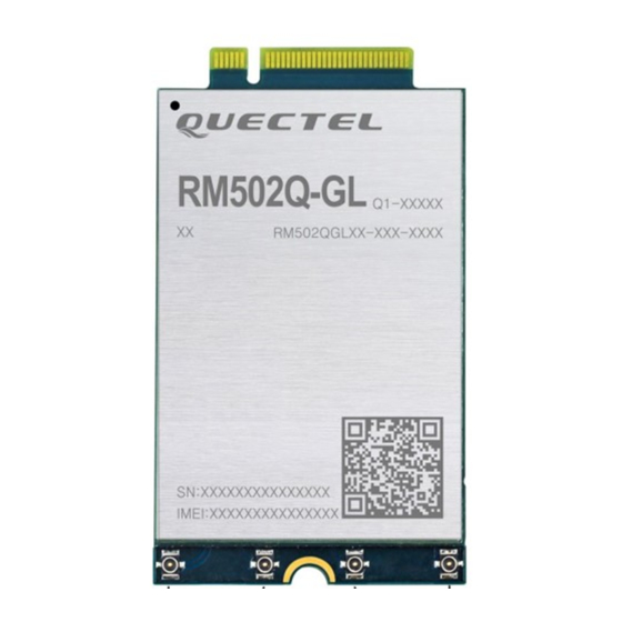
Page 75: Top And Bottom Views Of The Module
Bottom View Figure 42: Top and Bottom Views of the Module NOTE These are rendering images of RM502Q-GL module. For authentic appearance, please refer to the module that you receive from Quectel. 7.3. M.2 Connector RM502Q-GL adopts a standard PCI Express M.2 connector which compiles with the directives and standards listed in document [4]. -
Page 76: Packaging
5G Module Series RM502Q-GL Hardware Design 7.4. Packaging RM502Q-GL modules are packaged in trays. The following figure shows the tray size. Figure 43: Tray Size (Unit: mm) Each tray contains 10 modules. The smallest package contains 100 modules. Tray packaging procedures are as below. -
Page 77: Appendix References
5G Module Series RM502Q-GL Hardware Design Appendix References Table 38: Related Documents Document Name Remark Quectel_PCIe_Card_EVB_User_Guide PCIe card EVB user guide Quectel_RG500Q&RM502Q&RM510Q_AT_Commands_ AT commands manual for Manual RG500Q, RM502Q and RM510Q Quectel_RM502Q_GNSS_Application_Note RM502Q GNSS application note Quectel_RF_Layout_Application_Note RF layout application note... - Page 78 5G Module Series RM502Q-GL Hardware Design GLONASS Global Navigation Satellite System (Russia) GNSS Global Navigation Satellite System Global Positioning System Global System for Mobile Communications Half Rate HSPA High Speed Packet Access HSUPA High Speed Uplink Packet Access kbps Kilo Bits Per Second...
- Page 79 5G Module Series RM502Q-GL Hardware Design Radio Frequency Receive Specific Absorption Rate Short Message Service Transmit UART Universal Asynchronous Receiver & Transmitter Uplink Unsolicited Result Code Universal Serial Bus (U)SIM (Universal) Subscriber Identity Module Input High Voltage Level Input Low Voltage Level...
- Page 80 Quectel that they wish to change the antenna trace design. In this case, a Class II permissive change application is required to be filed by...
- Page 81 Antenna (1) The antenna must be installed such that 20 cm is maintained between the antenna and users, (2) The transmitter module may not be co-located with any other transmitter or antenna. In the event that these conditions cannot be met (for example certain laptop configurations or co-location with another transmitter), then the FCC/IC authorization is no longer considered valid and the FCC ID/IC ID cannot be used on the final product.
- Page 82 Federal Communication Commission Interference Statement This device complies with Part 15 of the FCC Rules. Operation is subject to the following two conditions: (1) This device may not cause harmful interference, and (2) this device must accept any interference received, including interference that may cause undesired operation. This equipment has been tested and found to comply with the limits for a Class B digital device, pursuant to Part 15 of the FCC Rules.
- Page 83 This device is intended only for OEM integrators under the following conditions: (For module device use) 1) The antenna must be installed such that 20 cm is maintained between the antenna and users, and 2) The transmitter module may not be co-located with any other transmitter or antenna. As long as 2 conditions above are met, further transmitter test will not be required.
- Page 84 Industry Canada Statement This device complies with Industry Canada’s licence-exempt RSSs. Operation is subject to the following two conditions: (1) This device may not cause interference; and (2) This device must accept any interference, including interference that may cause undesired operation of the device.
- Page 85 Cet appareil est conçu uniquement pour les intégrateurs OEM dans les conditions suivantes: (Pour utilisation de dispositif module) 1) L'antenne doit être installée de telle sorte qu'une distance de 20 cm est respectée entre l'antenne et les utilisateurs, et 2) Le module émetteur peut ne pas être coïmplanté avec un autre émetteur ou antenne. Tant que les 2 conditions ci-dessus sont remplies, des essais supplémentaires sur l'émetteur ne seront pas nécessaires.
- Page 86 Manual Information to the End User The OEM integrator has to be aware not to provide information to the end user regarding how to install or remove this RF module in the user’s manual of the end product which integrates this module. The end user manual shall include all required regulatory information/warning as show in this manual.
Need help?
Do you have a question about the RM502Q-GL and is the answer not in the manual?
Questions and answers