
Related Manuals for Quectel RM502Q-GL


Summary of Contents for Quectel RM502Q-GL
- Page 1 RM502Q-GL Hardware Design 5G Module Series Version: 1.0 Date: 2021-03-09 Status: Released www.quectel.com...
- Page 2 To the maximum extent permitted by law, Quectel excludes all liability for any loss or damage suffered in connection with the use of the functions and features under development, regardless of whether such loss or damage may have been foreseeable.
- Page 3 RM502Q-GL Hardware Design Copyright The information contained here is proprietary technical information of Quectel. Transmitting, reproducing, disseminating and editing this document as well as using the content without permission are forbidden. Offenders will be held liable for payment of damages. All rights are reserved in the event of a patent grant or registration of a utility model or design.
-
Page 4: Safety Information
Manufacturers of the cellular terminal should notify users and operating personnel of the following safety information by incorporating these guidelines into all manuals of the product. Otherwise, Quectel assumes no liability for customers’ failure to comply with these precautions. -
Page 5: About The Document
5G Module Series RM502Q-GL Hardware Design About the Document Revision History Version Date Author Description Norton ZHANG/ 2020-11-09 Creation of the document Qiqi WANG Norton ZHANG/ 2021-03-09 First official release Qiqi WANG RM502Q-GL_Hardware_Design 4 / 83... -
Page 6: Table Of Contents
5G Module Series RM502Q-GL Hardware Design Contents Safety Information ............................3 About the Document ........................... 4 Contents ............................... 5 Table Index ..............................8 Figure Index ............................... 10 Introduction ............................11 1.1. Introduction ..........................11 1.2. Reference Standard ........................11 1.3. - Page 7 5G Module Series RM502Q-GL Hardware Design 4.3. PCIe Interface ........................... 42 4.3.1. PCIe Operating Mode ....................42 4.3.2. Pin Definition of PCIe ..................... 43 4.3.3. Reference design of PCIe ....................44 4.3.4. PCIe Timing ........................45 4.4. PCM Interface ........................... 46 4.5.
- Page 8 5G Module Series RM502Q-GL Hardware Design 6.7. Operating and Storage Temperatures ..................77 Mechanical Dimensions and Packaging ..................78 7.1. Mechanical Dimensions of the Module ..................78 7.2. Top and Bottom Views of the Module ..................79 7.3. M.2 Connector ........................... 79 7.4.
- Page 9 RM502Q-GL Hardware Design Table Index Table 1: Special Mark..........................12 Table 2: Frequency Bands and GNSS Type of RM502Q-GL Module ............13 Table 3: Key Features ..........................14 Table 4: Definition of I/O Parameters ......................19 Table 5: Pin Description ..........................19 Table 6: Overview of Operation Modes .....................
- Page 10 5G Module Series RM502Q-GL Hardware Design Table 42: (U)SIM 1.8 V I/O Requirements ....................74 Table 43: (U)SIM 3.0V I/O Requirements ....................75 Table 44: Electrostatic Discharge Characteristics (Temperature: 25 º C, Humidity: 40 %) ....... 75 Table 45: Absolute Maximum Ratings ....................... 77 Table 46: Operating and Storage Temperatures ..................
- Page 11 Figure 27: Recommended Circuit for Configuration Pins ................55 Figure 28: Antenna Connectors on the Module ..................64 Figure 29: RM502Q-GL RF Connector Dimensions (Unit: mm) ..............65 Figure 30: Specifications of Mating Plugs Using Ø 0.81 mm Coaxial Cables ........... 66 Figure 31: Connection between RF Connector and Mating Plug Using Ø...
-
Page 12: Introduction
This document helps you quickly understand the interface specifications, electrical and mechanical details, as well as other related information of RM502Q-GL. To facilitate its application in different fields, reference design is also provided for reference. Coupled with application notes and user guides, you can easily design and set up mobile applications with RM502Q-GL. -
Page 13: Special Mark
5G Module Series RM502Q-GL Hardware Design 1.3. Special Mark Table 1: Special Mark Mark Definition When an asterisk (*) is used after a function, feature, interface, pin name, AT command, or argument, it indicates that the function, feature, interface, pin name, AT command, or argument is under development and currently not supported, unless otherwise specified. -
Page 14: Product Concept
RM502Q-GL is a 5G NR/LTE-FDD/LTE-TDD/WCDMA wireless communication module with receive diversity. It provides data connectivity on 5G NR SA and NSA, LTE-FDD, LTE-TDD ,DC-HSDPA, HSPA+, HSDPA, HSUPA, and WCDMA networks. RM502Q-GL is standard M.2 Key-B WWAN module. For more details, see PCI Express M.2 Specification Revision 3.0, Version 1.2. -
Page 15: Key Features
5G Module Series RM502Q-GL Hardware Design RM502Q-GL can be applied in the following fields: ⚫ Rugged tablet PC and laptop computer ⚫ Remote monitor system ⚫ Smart metering system ⚫ Wireless CPE ⚫ Smart TV ⚫ Outdoor Live devices ⚫... - Page 16 5G Module Series RM502Q-GL Hardware Design synchronization ⚫ WCDMA bands: Class 3 (24 dBm +1/-3 dB) ⚫ LTE-FDD bands: Class 3 (23 dBm ± 2 dB) ⚫ LTE-TDD bands: Class 3 (23 dBm ± 2 dB) Transmitting Power ⚫ LTE B38/B40/B41/B42/B43 bands HPUE : Class 2 (26 dBm ±...
- Page 17 5G Module Series RM502Q-GL Hardware Design ⚫ Quectel enhanced AT commands ⚫ Internet Protocol Supports QMI/NTP* protocols ⚫ Features Supports PAP and CHAP, usually used for PPP connections ⚫ USB 2.0 interface ⚫ Firmware Upgrade PCIe interface ⚫ DFOTA ⚫...
-
Page 18: Evaluation Board
RM502Q-GL Hardware Design 2.3. Evaluation Board To help you develop applications conveniently with RM502Q-GL, Quectel supplies an evaluation board (PCIe Card EVB), a USB to RS-232 converter cable, a USB type-B cable, antennas and other peripherals to control or test the module. For more details, see document [3]. -
Page 19: Pin Assignment
5G Module Series RM502Q-GL Hardware Design 2.5. Pin Assignment The following figure shows the pin assignment of RM502Q-GL. And the top side contains the four antenna connectors. Pin Name Pin Name CONFIG_2 CONFIG_1 AP2SDX_STATUS RESET# USIM1_DET RFFE_VIO_1V8 COEX_TXD PIN75 PIN74... -
Page 20: Pin Description
Digital Input Digital Output Digital Input/Output Open Drain Power Input Power Output Pull Up Pull Down The following table shows the pin definition and description of RM502Q-GL. Table 5: Pin Description Pin Name Description Comment Characteristic Not connected CONFIG_3 internally Vmin = 3.135 V... - Page 21 5G Module Series RM502Q-GL Hardware Design Ground Turn on/off of the max = 4.4 V Internally pulled FULL_CARD_ module. min = 1.19 V down with a POWER_OFF# High level: Turn on 100 kΩ resistor max = 0.2 V Low level: Turn off USB 2.0 differential...
- Page 22 5G Module Series RM502Q-GL Hardware Design GNSS disable W_DISABLE2# DI, OD control. 1.8/3.3 V Active LOW. Ground PCM_SYNC DIO, PD PCM data frame sync 1.8 V USB 3.1 super-speed USB_SS_TX_M transmit (-) USIM1_VDD USIM1_RST DO, PD (U)SIM1 card reset 1.8/3.0 V USB 3.1 super-speed...
- Page 23 5G Module Series RM502Q-GL Hardware Design 1.8/3.0 V PCIE_RX_M PCIe receive (-) Power supply for USIM1_VDD USIM2_VDD (U)SIM2 card 1.8/3.0 V PCIE_RX_P PCIe receive (+) PCIe reset. PCIE_RST_N DI, OD Active LOW. Ground PCIe clock request. PCIE_CLKREQ_N DO, OD Active LOW.
- Page 24 This pin is pulled LOW by default, and will be internally pulled up to 1.8 V by software configuration 、 only when (U)SIM hot-plug is enabled by AT+QSIMDET. If this function is required, please contact Quectel for more details. 3. Keep all NC, reserved and unused pins unconnected. RM502Q-GL_Hardware_Design...
-
Page 25: Operating Characteristics
5G Module Series RM502Q-GL Hardware Design Operating Characteristics 3.1. Operating Modes The table below briefly summarizes the various operating modes to be mentioned in the following chapters. Table 6: Overview of Operation Modes Mode Details Software is active. The module has registered on the network, and it is Idle ready to send and receive data. - Page 26 5G Module Series RM502Q-GL Hardware Design DRX OFF Run Time Figure 3: DRX Run Time and Current Consumption in Sleep Mode The following part of this section presents the power saving procedure and sleep mode of the module. If the host supports USB suspend/resume and remote wakeup function, the following two conditions must be met to make the module enter sleep mode.
-
Page 27: Airplane Mode
Supports Non-X86 systems and X86 system (supports BIOS PCIe early initial) RM502Q-GL can also be reprogrammed to PCIe mode based on eFuse. If the communication is switched to PCIe mode by burnt eFuse, the communication cannot be switched back to USB mode. -
Page 28: Power Supply
5G Module Series RM502Q-GL Hardware Design 3.3. Power Supply The following table shows pin definition of VCC pins and ground pins. Table 7: Definition of VCC and GND Pins Pin No. Pin Name Description DC Characteristics 3.135–4.4 V 2, 4, 70, 72, 74 Power Supply 3.7 V typical DC supply... -
Page 29: Reference Design For Power Supply
5G Module Series RM502Q-GL Hardware Design Module VCC (3.7 V Typ.) 2, 4 220 μF 1 μF 100 nF 33 pF 10 pF 3, 5, 11 70, 72, 74 220 μF 1 μF 5.1 V 100 nF 33 pF 10 pF... -
Page 30: Monitor The Power Supply
5G Module Series RM502Q-GL Hardware Design NOTE To avoid damages to the internal flash, DON'T cut off the power supply before the module is completely turned off by pulling down FULL_CARD_POWER_OFF# pin for more than 7 s, and DON'T cut off power supply directly when the module is working. - Page 31 5G Module Series RM502Q-GL Hardware Design It is recommended to use a host GPIO to control FULL_CARD_POWER_OFF#. A simple reference circuit is illustrated by the following figure. Host Module 1.8 V or 3.3 V FULL_CARD_POWER_OFF# GPIO 100k NOTE: The voltage of pin 6 should be no less than 1.19 V when it is at HIGH level.
-
Page 32: Turn Off
5G Module Series RM502Q-GL Hardware Design Table 9: Turn-on Timing of the Module Symbol Min. Typ. Max. Comment 0 ms 20 ms Module power-on time depending on the host. power-on Time period between module power-on and 33 ms VCC-RST# RESET# being driven HIGH. -
Page 33: Turn Off The Module Through At Command
5G Module Series RM502Q-GL Hardware Design Table 10: Turn-off Timing of the Module Through FCPO# Symbol Min. Typ. Max. Comment 6.84 s Module system turn-off time. turn-off 3.5.2. Turn off the Module Through AT Command It is also a safe way to use AT+QPOWD command to turn off the module. For more details about the command, see document [4]. -
Page 34: Reset
5G Module Series RM502Q-GL Hardware Design 3.6. Reset RESET# is an asynchronous and active LOW signal (1.8 V logic level). Whenever this pin is active, the module will immediately enter Power On Reset (POR) condition. Please note that triggering the RESET# signal will lead to loss of all data in the modem and removal of system drivers. - Page 35 5G Module Series RM502Q-GL Hardware Design Module VDD 1.8V 100k RESET# PMIC 33 pF 200-980 ms NOTE: The capacitor C1 is recommended to be less than 47 pF. Figure 13: Reference Circuit of RESET# with Button The reset timing is illustrated by the following figure.
-
Page 36: Application Interfaces
5G Module Series RM502Q-GL Hardware Design Application Interfaces The physical connections and signal levels of RM502Q-GL comply with PCI Express M.2 specification. This chapter mainly describes the definition and application of the following interfaces/pins of the module: ⚫ (U)SIM interfaces ⚫... -
Page 37: Hot-Plug Of (U)Sim
5G Module Series RM502Q-GL Hardware Design USIM1_DET DI, PU (U)SIM1 card hot-plug detect USIM2_VDD Power supply for (U)SIM2 card 1.8/3.0 V USIM2_VDD USIM2_DATA DIO, PU (U)SIM2 card data 1.8/3.0 V USIM2_VDD USIM2_CLK DO, PD (U)SIM2 card clock 1.8/3.0 V USIM2_VDD... -
Page 38: Normally Closed (U)Sim Card Connector
5G Module Series RM502Q-GL Hardware Design The command takes effect after the module is restarted. Characteristics The configuration will be saved automatically. Parameter <enable> Integer type. Enable or disable (U)SIM card detection. Disable Enable <insert_level> Integer type. The level of (U)SIM detection pin when a (U)SIM card is inserted. -
Page 39: Normally Open (U)Sim Card Connector
5G Module Series RM502Q-GL Hardware Design The following figure shows a reference design for (U)SIM interface with a normally closed (U)SIM card connector. USIM_VDD Module (U)SIM Card Connector 100 nF 10-20k USIM_VDD USIM_RST USIM_CLK USIM_DET USIM_DATA NOTE: All these resistors, capacitors and TVS should be close to (U)SIM card connector in PCB layout. -
Page 40: U)Sim Card Connector Without Hot-Plug
5G Module Series RM502Q-GL Hardware Design The following figure shows a reference design for (U)SIM interface with a normally open (NO) (U)SIM card connector. USIM_VDD Module (U)SIM Card Connector 100 nF 10-20k USIM_VDD USIM_RST USIM_CLK USIM_DET 0 Ω USIM_DATA NOTE: All these resistors, capacitors and TVS should be close to (U)SIM card connector in PCB layout. -
Page 41: U)Sim Design Notices
For USIM_DATA, a 10–20 kΩ pull-up resistor must be added near the (U)SIM card connector. 4.2. USB Interface RM502Q-GL provides one integrated Universal Serial Bus (USB) interface which complies with the USB 3.1/2.0 specifications and supports super speed (10 Gbps) on USB 3.1 and high speed (480 Mbps) and full speed (12 Mbps) modes on USB 2.0. - Page 42 5G Module Series RM502Q-GL Hardware Design USB_SS_RX_P USB 3.1 super-speed receive (+) For more details about the USB 3.1 & 2.0 specifications, please visit http://www.usb.org/home. The USB 2.0 interface is recommended to be reserved for firmware upgrade in designs. The following figure shows a reference circuit for USB 2.0/3.1 interface.
-
Page 43: Pcie Interface
Keep the ESD protection devices as close to the USB connector as possible. ⚫ If possible, reserve 0 Ω resistors on USB_DP and USB_DM lines respectively. 4.3. PCIe Interface RM502Q-GL provides one integrated PCIe (Peripheral Component Interconnect Express) interface. ⚫ PCI Express Base Specification Revision 3.0 compliant ⚫... -
Page 44: Pin Definition Of Pcie
5G Module Series RM502Q-GL Hardware Design NOTES The underlined value is the default parameter value. For more details about the command, see document [4]. 4.3.2. Pin Definition of PCIe The following table shows the pin definition of PCIe interface. Table 16: Pin Definition of PCIe Interface Pin No. -
Page 45: Reference Design Of Pcie
5G Module Series RM502Q-GL Hardware Design 4.3.3. Reference design of PCIe The following figure shows a reference circuit for the PCIe interface. Host Module PCIE_REFCLK_P R4 0Ω PCIE_REFCLK_P PCIE_REFCLK_M R5 0Ω PCIE_REFCLK_M PCIE_RX_P C3 220 nF PCIE_TX_P PCIE_RX_M C4 220 nF... -
Page 46: Pcie Timing
5G Module Series RM502Q-GL Hardware Design 4.3.4. PCIe Timing The following figure is PCIe power-up timing sequence for an adapter powered from system power rail in PCI Express M.2 specification. Figure 20: PCIe Power-up Timing of M.2 Specification The following table is power-up timing variables in PCI Express M.2 specification. -
Page 47: Pcm Interface
5G Module Series RM502Q-GL Hardware Design The following figure and table are PCIe turn-on timing and variables of the module. Module power-on or insertion detection 3.7 V ≥ 1.19 V System turn-on and booting FCPO# 1.8 V VCC-RST# RESET# 1.8 V RFFE_VIO_1V8 >... - Page 48 5G Module Series RM502Q-GL Hardware Design ⚫ Primary mode (short frame synchronization): the module works as both master and slave ⚫ Auxiliary mode (long frame synchronization): the module works as master only In primary mode, the data is sampled on the falling edge of the PCM_CLK and transmitted on the rising edge.
- Page 49 5G Module Series RM502Q-GL Hardware Design 125 μs PCM_CLK PCM_SYNC PCM_DOUT PCM_DIN Figure 23: Auxiliary Mode Timing The following table shows the pin definition of PCM interface which can be applied to audio codec design. Table 19: Pin Definition of PCM Interface Pin No.
-
Page 50: Control And Indication Interfaces
5G Module Series RM502Q-GL Hardware Design 4.5. Control and Indication Interfaces The following table shows the pin definition of control and indication pins. Table 20: Pin Definition of Control and Indication Interfaces Pin No. Pin Name Description DC Characteristic Airplane mode control. -
Page 51: W_Disable2
5G Module Series RM502Q-GL Hardware Design AT+CFUN=0 AT+CFUN=1 Disabled AT+CFUN=4 4.5.2. W_DISABLE2# The module provides a W_DISABLE2# pin to disable or enable the GNSS function. The W_DISABLE2# pin is pulled up by default. Driving it low will disable the GNSS function. The combination of W_DISABLE2# pin and AT commands controls the GNSS function. -
Page 52: Wwan_Led
5G Module Series RM502Q-GL Hardware Design 4.5.3. WWAN_LED# WWAN_LED# signal is used to indicate the RF status of the module, and its sink current is up to 10 mA. To reduce current consumption of the LED, a current-limited resistor must be placed in series with the LED, as illustrated by the figure below. -
Page 53: Dpr
RM502Q-GL provides a DPR (Dynamic Power Reduction) pin for body SAR (Specific Absorption Rate) detection. The signal is sent from the proximity sensor of a host system to RM502Q-GL module to provide an input trigger, which will reduce the output power in radio transmission. -
Page 54: Status
(SDX2AP_STATUS) outputs the status indication signal to IPQ807x device, and pin 68 (AP2SDX_STATUS) inputs the status indication signal from IPQ807x device. 4.6. Cellular/WLAN COEX Interface* RM502Q-GL provides a cellular/WLAN COEX interface, the following table shows the pin definition of this interface. Table 26: Pin Definition of COEX Interface Pin No. -
Page 55: Configuration Pins
Antenna GPIO Control ANTCTL2* DO, PD 1.8 V NOTE If this function is required, please contact Quectel for more details. 4.8. Configuration Pins RM502Q-GL provides four configuration pins, which are defined as below. Table 28: Configuration Pins List of M.2 Specification Config_0... - Page 56 5G Module Series RM502Q-GL Hardware Design The following figure shows a reference circuit for these four pins. Host Module VCC_IO_HOST NM-0Ω CONFIG_0 GPIO 0Ω CONFIG_1 GPIO NM-0Ω CONFIG_2 GPIO CONFIG_3 NM-0Ω GPIO NOTE: The voltage level of VCC_IO_HOST depends on the host side and could be 1.8 V or 3.3 V.
-
Page 57: Rf Characteristic
The chapter mainly describes RF characteristics of RM502Q-GL. 5.1. Cellular Antenna Interfaces 5.1.1. Pin Definition The pin definition of antenna interfaces is shown below. Table 30: RF Bands Supported by RM502Q-GL Antenna Connectors Pin Name Description Frequency Antenna 0 interface:... -
Page 58: Pin Mapping
5G Module Series RM502Q-GL Hardware Design 5.1.2. Pin Mapping Table 31: RM502Q-GL Cellular Antenna Mapping 5G NR n77/n78 Antenna WCDMA/LTE MHB (MHz) (MHz) (MHz) Refarmed n77/n78 LTE LMHB TRX; ANT0 LMHB TRX TRX1 TRX1 LTE UHB PRX MIMO 617–960 1452–2690 3300–4200... - Page 59 5G Module Series RM502Q-GL Hardware Design – EGSM (950) 880–915 925–960 – – – – J1700 1750–1785 1845–1880 – – 700 lower A–C 699–716 729–746 – – – 700 upper C 777–787 746–756 – – – 700 D 788–798 758–768 –...
-
Page 60: Receiving Sensitivity
– 3300–4200 3300–4200 – – – 3300–3800 3300–3800 5.1.4. Receiving Sensitivity The following tables show conducted RF receiving sensitivity of the module. Table 33: RM502Q-GL Conducted RF Receiving Sensitivity Mode Frequency Primary Diversity SIMO 3GPP (SIMO) WCDMA B1 -109 -110 -112 -106.7 dBm... - Page 61 5G Module Series RM502Q-GL Hardware Design LTE-FDD B18 (10 MHz) -100 -101 -103 -96.3 dBm LTE-FDD B19 (10 MHz) -100 -101 -103 -96.3 dBm LTE-FDD B20 (10 MHz) -100 -101 -103 -93.3 dBm LTE-FDD B25 (10 MHz) -101 -92.8 dBm LTE-FDD B26 (10 MHz) -99.5...
-
Page 62: Output Power
5G Module Series RM502Q-GL Hardware Design 5G NR-FDD n12 (10 MHz) -99.5 -94.0 dBm (SCS: 15 kHz) 5G NR-FDD n20 (10 MHz) -95.5 -99.5 -94.0 dBm (SCS: 15 kHz) 5G NR-FDD n25 (20 MHz) -92.5 -90.5 dBm (SCS: 15 kHz) 5G NR-FDD n28 (10 MHz) -96.5... -
Page 63: Gnss Antenna Interface
5G Module Series RM502Q-GL Hardware Design LTE HPUE bands 26 dBm ± 2 dB (Class 2) < -40 dBm (B38/B40/B41/B42/B43) < -40 dBm 5G NR bands 23 dBm ± 2 dB (Class 3) (BW: 5–20 MHz) 5G NR 5G NR HPUE bands <... -
Page 64: Gnss Performance
Keep 15 dB isolation between each antenna to improve the receiving sensitivity. and 20 dB isolation between 5G NR UL MIMO TRX0 and TRX1 antennas. 5.2.3. GNSS Performance The following table shows GNSS performance of RM502Q-GL series module. Table 36: GNSS Performance Parameter Description Conditions Typ. -
Page 65: Antenna Connectors
Cold start sensitivity: the minimum GNSS signal power at which the module can fix position successfully within 3 minutes after executing cold start command. 5.3. Antenna Connectors 5.3.1. Antenna Connector Location RM502Q-GL has four antenna connectors: ANT0, ANT1, ANT2_GNSSL1 and ANT3, which are shown below. Figure 28: Antenna Connectors on the Module RM502Q-GL_Hardware_Design... -
Page 66: Antenna Connector Size
5G Module Series RM502Q-GL Hardware Design 5.3.2. Antenna Connector Size RM502Q-GL is mounted with standard 2 mm × 2 mm receptacle antenna connectors for convenient antenna connection. The antenna connector’s PN is IPEX 20579-001E, and the connector dimensions are illustrated as below:... -
Page 67: Antenna Connector Installation
5.3.3. Antenna Connector Installation The receptacle RF connector used in conjunction with RM502Q-GL will accept two types of mating plugs that will meet a maximum height of 1.2 mm using a Ø 0.81 mm coaxial cable or a maximum height of 1.45 mm utilizing a Ø... -
Page 68: Recommended Rf Connector For Installation
5G Module Series RM502Q-GL Hardware Design The following figure illustrates the connection between the receptacle RF connector on RM502Q-GL and the mating plug using a Ø 1.13 mm coaxial cable. Figure 32: Connection between RF Connector and Mating Plug Using Ø 1.13 mm Coaxial Cable 5.3.4. -
Page 69: Assemble Coaxial Cable Plug With Jig
5G Module Series RM502Q-GL Hardware Design The pictures of pulling out the coaxial cable plug is shown below, θ = 90° is acceptable, while θ ≠ 90° is not. Figure 34: Pull out a Coaxial Cable Plug 5.3.4.2. Assemble Coaxial Cable Plug with Jig The pictures of installing the coaxial cable plug with a jig is shown below, θ... -
Page 70: Recommended Manufacturers Of Rf Connector And Cable
5G Module Series RM502Q-GL Hardware Design 5.3.5. Recommended Manufacturers of RF Connector and Cable RF connecters and cables by I-PEX are recommended. For more details, visit https://www.i-pex.com. 5.4. Antenna Requirements The following table shows the requirements on WCDMA, LTE, 5G NR antenna and GNSS antenna. -
Page 71: Electrical Characteristics And Reliability
Table 39: Power Supply Requirement Parameter Description Min. Typ. Max. Unit Power Supply 3.135 Voltage Ripple Voltage Drop 6.2. Current Consumption Table 40: RM502Q-GL Current Consumption Description Conditions Typ. Unit μA OFF state Power down 71.8 AT+CFUN=0 @ USB Suspend 3.91 Sleep state WCDMA PF = 64 @ USB Suspend 4.83... - Page 72 5G Module Series RM502Q-GL Hardware Design LTE-TDD PF = 64 @ USB Suspend 5.50 WCDMA PF = 64 (USB disconnected) 31.43 WCDMA PF = 64 (USB connected) 53.18 LTE-FDD PF = 64 (USB disconnected) 29.41 Idle state LTE-FDD PF = 64 (USB connected) 50.86...
- Page 73 5G Module Series RM502Q-GL Hardware Design LTE-FDD B3 CH1575 @ 23 dBm LTE-FDD B4 CH2175 @ 23 dBm LTE-FDD B5 CH2525 @ 23 dBm LTE-FDD B7 CH3100 @ 23 dBm LTE-FDD B8 CH3625 @ 23 dBm LTE-FDD B12 CH5095 @ 23 dBm...
- Page 74 5G Module Series RM502Q-GL Hardware Design LTE-FDD B71 CH68761 @ 23 dBm 5G NR-TDD n41 CH518598 @ 26 dBm 5G NR-TDD n77 CH650000 @ 26 dBm 5G NR-TDD n78 CH636666 @ 26 dBm 5G NR-FDD n1 CH428000 @ 23 dBm...
-
Page 75: Digital I/O Characteristic
5G Module Series RM502Q-GL Hardware Design WCDMA B8 CH3012 @ 23 dBm WCDMA B19 CH338 @ 23 dBm NOTE For the current comsuption of 5G NR, the test is based on CP-OFDM QPSK mode. 6.3. Digital I/O Characteristic Table 41: Logic Levels of Digital I/O (1.8 V) -
Page 76: Electrostatic Discharge
5G Module Series RM502Q-GL Hardware Design Table 43: (U)SIM 3.0V I/O Requirements Parameter Description Min. Max. Unit USIM_VDD Power supply 3.05 Input high voltage 0.7 × USIM_VDD USIM_VDD + 0.3 Input low voltage -0.3 0.2 × USIM_VDD Output high voltage 0.8 ×... - Page 77 5G Module Series RM502Q-GL Hardware Design Figure 36: Thermal Dissipation Area Inside and on Bottom Side of the Module (Unit: mm) There are other measures to enhance heat dissipation performance: ⚫ Add as many ground vias as possible on PCB.
-
Page 78: Absolute Maximum Ratings
5G Module Series RM502Q-GL Hardware Design 6.6. Absolute Maximum Ratings Absolute maximum ratings for power supply and voltage on digital and analog pins of the module are listed in the following table. Table 45: Absolute Maximum Ratings Parameter Min. Typ. -
Page 79: Mechanical Dimensions And Packaging
5G Module Series RM502Q-GL Hardware Design Mechanical Dimensions and Packaging This chapter mainly describes mechanical dimensions and packaging specifications of the module. All dimensions are measured in mm, and the tolerances are ± 0.05 mm unless otherwise specified. 7.1. Mechanical Dimensions of the Module... -
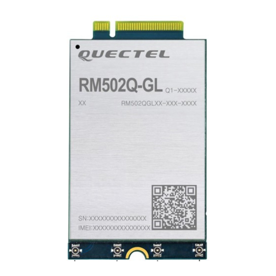
Page 80: Top And Bottom Views Of The Module
NOTE Images above are for illustration purpose only and may differ from the actual module. For authentic appearance and label, please refer to the module received from Quectel. 7.3. M.2 Connector The module adopts a standard PCI Express M.2 connector which compiles with the directives and standards listed in PCI Express M.2 Specification Revision 3.0, Version 1.2. -
Page 81: Packaging
5G Module Series RM502Q-GL Hardware Design 7.4. Packaging RM502Q-GL modules are packaged in trays. The following figure shows the tray size. Figure 39: Tray Size (Unit: mm) Each tray contains 10 modules. The smallest package contains 100 modules. Tray packaging procedures are as below. -
Page 82: Appendix References
5G Module Series RM502Q-GL Hardware Design Appendix References Table 47: Related Documents Document Name Description Quectel_RM50xQ_Series_Reference_Design Reference design for RM502Q-GL CA&EN-DC features for Quectel_RM50xQ-GL_CA&EN-DC_Features RM502Q-GL Quectel_PCIe_Card_EVB_User_Guide PCIe card EVB user guide Quectel_RG50xQ&RM5xxQ_Series_AT_Commands AT commands manual for RG50xQ _Manual and RM5xxQ series Quectel_RG50xQ&RM5xxQ_Series_GNSS_Application... - Page 83 5G Module Series RM502Q-GL Hardware Design Electromagnetic Interference Electrostatic Discharge Equivalent Series Resistance ETSI European Telecommunications Standards Institute Frequency Division Duplexing GLONASS Global Navigation Satellite System (Russia) GNSS Global Navigation Satellite System GPIO General-Purpose Input/Output Global Positioning System Global System for Mobile Communications...
- Page 84 5G Module Series RM502Q-GL Hardware Design Password Authentication Protocol Printed Circuit Board PCIe Peripheral Component Interconnect Express Pulse Code Modulation Protocol Data Unit Paging Frame Point-to-Point Protocol Quadrature Amplitude Modulation QPSK Quadrature Phase Shift Keying QZSS Quasi-Zenith Satellite System Radio Frequency...
Need help?
Do you have a question about the RM502Q-GL and is the answer not in the manual?
Questions and answers