
Related Manuals for Quectel RM510Q-GL


Summary of Contents for Quectel RM510Q-GL
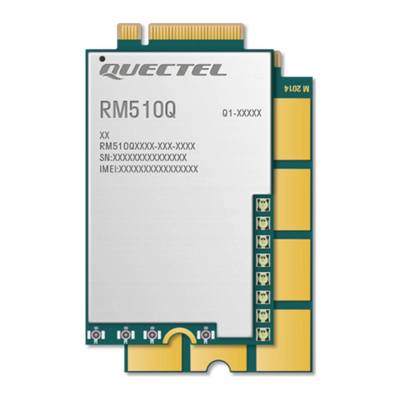
- Page 1 RM510Q-GL Hardware Design 5G Module Series Version: 1.0 Date: 2021-02-07 Status: Released www.quectel.com...
- Page 2 To the maximum extent permitted by law, Quectel excludes all liability for any loss or damage suffered in connection with the use of the functions and features under development, regardless of whether such loss or damage may have been foreseeable.
- Page 3 RM510Q-GL Hardware Design Copyright The information contained here is proprietary technical information of Quectel wireless solutions co., ltd. Transmitting, reproducing, disseminating and editing this document as well as using the content without permission are forbidden. Offenders will be held liable for payment of damages. All rights are reserved in the event of a patent grant or registration of a utility model or design.
-
Page 4: Safety Information
Manufacturers of the cellular terminal should notify users and operating personnel of the following safety information by incorporating these guidelines into all manuals of the product. Otherwise, Quectel assumes no liability for customers’ failure to comply with these precautions. -
Page 5: About The Document
5G Module Series RM510Q-GL Hardware Design About the Document Revision History Version Date Author Description Kingson ZHANG 2020-10-22 Creation of the document /Jumping HE Kingson ZHANG 2021-02-07 First official release /Jumping HE RM510Q-GL_Hardware_Design 4 / 88... -
Page 6: Table Of Contents
5G Module Series RM510Q-GL Hardware Design Contents Safety Information ............................3 About the Document ........................... 4 Contents ............................... 5 Table Index ..............................8 Figure Index ............................... 10 Introduction ............................12 1.1. Introduction ..........................12 1.2. Reference Standard ........................12 1.3. - Page 7 5G Module Series RM510Q-GL Hardware Design 4.1.5. Without Hot-plug (U)SIM Card Connector ..............39 4.1.6. (U)SIM Design Notices....................39 4.2. USB Interface ..........................40 4.3. PCIe Interface ........................... 42 4.3.1. PCIe Operating Mode ....................42 4.3.2. Pin Definition of PCIe ..................... 42 4.3.3.
- Page 8 5G Module Series RM510Q-GL Hardware Design 5.4.4. Recommended RF Connector for Installation ............... 69 5.4.4.1. Assemble Coaxial Cable Plug Manually ............. 69 5.4.4.2. Assemble Coaxial Cable Plug with Jig ............... 70 5.4.5. Recommended Manufacturers of RF Connector and Cable ......... 71 5.5.
- Page 9 RM510Q-GL Hardware Design Table Index Table 1: Special Mark..........................13 Table 1: Frequency Bands and GNSS Type of RM510Q-GL Module ............14 Table 2: Key Features of RM510Q-GL ...................... 15 Table 3: Definition of I/O Parameters ......................20 Table 4: Pin Description ..........................20 Table 5: Overview of Operating Modes .....................
- Page 10 5G Module Series RM510Q-GL Hardware Design Table 41: Major Specifications of the RF Connector ................. 67 Table 42: Cellular Bands Supported by RM510Q-GL Antenna Connectors ..........71 Table 43: Antenna Requirements ......................71 Table 44: Power Supply Requirements ..................... 73 Table 45: RM510Q-GL Current Consumption ...................
- Page 11 Figure 38: Thermal Dissipation Area on Bottom Side of Module .............. 80 Figure 39: Mechanical Dimensions of the Module (Unit: mm) ..............83 Figure 40: RM510Q-GL Top View and Bottom View ................. 84 Figure 41: Tray Size (Unit: mm) ......................... 85...
- Page 12 5G Module Series RM510Q-GL Hardware Design Figure 42: Tray Packaging Procedure ....................... 85 RM510Q-GL_Hardware_Design 11 / 88...
-
Page 13: Introduction
This document helps you quickly understand the interface specifications, electrical and mechanical details, as well as other related information of RM510Q-GL. To facilitate its application in different fields, reference design is also provided for reference. Associated with application notes and user guides, customers can use the module to design and set up mobile applications easily. -
Page 14: Special Mark
5G Module Series RM510Q-GL Hardware Design 1.3. Special Mark Table 1: Special Mark Mark Definition When an asterisk (*) is used after a function, feature, interface, pin name, AT command, or argument, it indicates that the function, feature, interface, pin name, AT command, or argument is under development and currently not supported, unless otherwise specified. -
Page 15: Product Concept
HSDPA, HSUPA and WCDMA networks. It is a standard M.2 Key-B WWAN module. For more details, see PCI Express M.2 Specification Revision 3.0, Version 1.2. RM510Q-GL is an industrial-grade module for industrial and commercial applications only. It supports embedded operating systems such as Windows, Linux and Android, and also provide GNSS and voice functionality to meet specific application demands. -
Page 16: Key Features
Outdoor live devices ⚫ Wireless r outer and switch ⚫ Other wireless terminal devices 2.2. Key Features The following table describes key features of RM510Q-GL. Table 3: Key Features of RM510Q-GL Feature Details Function Interface PCI Express M.2 Interface ⚫... - Page 17 5G Module Series RM510Q-GL Hardware Design ⚫ Used for audio function with external codec ⚫ Support 16-bit linear data format ⚫ Support long and short frame synchronization ⚫ Support master and slave modes, but must be the master in long frame synchronization ⚫...
- Page 18 5G Module Series RM510Q-GL Hardware Design HSUPA: Max 5.76 Mbps (UL) WCDMA: Max 384 kbps (DL)/384 kbps (UL) ⚫ Rx-diversity Supports 5G NR/LTE/WCDMA Rx-diversity ⚫ Protocol: NMEA 0183 GNSS Features ⚫ Data Update Rate: 1 Hz ⚫ Antenna Interfaces ANT0, ANT1, ANT2, and ANT3_GNSSL1 ⚫...
-
Page 19: Evaluation Board
RM510Q-GL Hardware Design 2.3. Evaluation Board To help you develop applications conveniently with the module, Quectel supplies an evaluation board (5G-mmWave-EVB), a USB micro-B cable, a USB type-C cable, antennas and other peripherals to control or test the module. For more details, see document [2] & document [3]. -
Page 20: Pin Assignment
5G Module Series RM510Q-GL Hardware Design 2.5. Pin Assignment The following figure shows the pin assignment of the module. The top side contains module and antenna connectors. Pin Name Pin Name CONFIG_2 CONFIG_1 AP2SDX_STATUS RESET# PIN75 USIM1_DET PIN74 RFFE_VIO_1V8 COEX_TXD... -
Page 21: Pin Description
5G Module Series RM510Q-GL Hardware Design 2.6. Pin Description Table 4: Definition of I/O Parameters Type Description Analog Input Analog Output Analog Input/Output Digital Input Digital Output Digital Input/Output Open Drain Power Input Power Output Pull Up Pull Down The following table shows the pin definition and description of the module. - Page 22 5G Module Series RM510Q-GL Hardware Design Ground Turn on/off the module. max = 4.4 V Internally pulled FULL_CARD_ DI, PD High level: Turn on min = 1.19 V down with a 100 POWER_OFF# kΩ resistor. Low level: Turn off max = 0.2 V USB 2.0 differential...
- Page 23 5G Module Series RM510Q-GL Hardware Design Ground PCM_SYNC DI, PD PCM data frame sync 1.8 V USB 3.1 super-speed USB_SS_TX_M transmit (-) USIM_VDD USIM1_RST DO, PD (U)SIM1 card reset 1.8/3.0 V USB 3.1 super-speed USB_SS_TX_P transmit (+) USIM_VDD USIM1_CLK DO, PD (U)SIM1 clock 1.8/3.0 V...
- Page 24 5G Module Series RM510Q-GL Hardware Design PCIE_RX_P PCIe receive (+) PCIe reset. PCIE_RST_N DI, OD Active LOW Ground PCIe clock request. PCIE_CLKREQ_N DO, OD Active LOW PCIE_REFCLK_M AI, AO PCIe reference clock (-) PCIe wake up PCIE_WAKE_N DO, OD Active LOW...
- Page 25 5G Module Series RM510Q-GL Hardware Design internally Vmin = 3.135 V Power supply Vnom = 3.7 V Vmax = 4.4 V Ground Vmin = 3.135 V Power supply Vnom = 3.7 V Vmax = 4.4 V Ground Vmin = 3.135 V Power supply Vnom = 3.7 V...
-
Page 26: Operating Characteristics
5G Module Series RM510Q-GL Hardware Design Operating Characteristics 3.1. Operating Modes The table below briefly summarizes the various operating modes to be mentioned in the following chapters. Table 6: Overview of Operating Modes Mode Details Software is active. The module has registered on the network, and it is Idle ready to send and receive data. - Page 27 5G Module Series RM510Q-GL Hardware Design Figure 3: DRX Run Time and Current Consumption in Sleep Mode The following section describes power saving procedure of module. If the host supports USB suspend/resume and remote wakeup function, the following two preconditions must be met to enable the module enter sleep mode.
-
Page 28: Airplane Mode
Supports Non-X86 systems and X86 system (supports BIOS PCIe early initial) RM510Q-GL can also be reprogrammed to PCIe mode based on eFuse. If the communication is switched to PCIe mode by burnt eFuse, the communication cannot be switched back to USB mode. -
Page 29: Power Supply
5G Module Series RM510Q-GL Hardware Design 3.3. Power Supply The following table shows pin definition of VCC pins and ground pins. Table 7: Definition of VCC and GND Pins Pin Name Description DC Characteristics 3.135–4.4 V 2, 4, 70, 72, 74 Power supply 3.7 V typical DC supply... -
Page 30: Reference Design For Power Supply
5G Module Series RM510Q-GL Hardware Design Module VCC (3.7 V Typ.) 2, 4 100 μ F 1 μ F 100 nF 33 pF 10 pF 3, 5, 11 70, 72, 74 100 μ F 1 μ F 5.1 V 100 nF... -
Page 31: Monitor The Power Supply
5G Module Series RM510Q-GL Hardware Design NOTE To avoid damages to the internal flash, please cut off power supply after the module is turned off by pulling down FULL_CARD_POWER_OFF# pin for more than 7 s, and DON'T cut off power supply directly when the module is working. - Page 32 5G Module Series RM510Q-GL Hardware Design Host Module 1.8 V or 3.3 V FULL_CARD_POWER_OFF# GPIO PMIC 100k Note: The voltage of pin 6 should be no less than 1.19V when it is at HIGH level. Figure 8: Turn on the Module with a Host GPIO The timing of turn-on scenario is illustrated in the following figure.
-
Page 33: Turn Off
5G Module Series RM510Q-GL Hardware Design 3.5. Turn off 3.5.1. Turn off the Module through FULL_CARD_POWER_OFF# For the design that turns on the module with a host GPIO, when the power is supplied to VCC, pulling down FULL_CARD_POWER_OFF# will turn off the module. -
Page 34: Reset
5G Module Series RM510Q-GL Hardware Design 3.7 V 1.5 V ≥ 1.19 V 1.8 V 1.8 V or 3.0 V AT+QPOWD USB/PCIe removed Running Turn-off procedure turn-off Figure 11: Turn-off Timing through AT Command and FULL_CARD_POWER_OFF# Table 11: Turn-off Time through AT Command and FULL_CARD_POWER_OFF# Symbol Min. - Page 35 5G Module Series RM510Q-GL Hardware Design NOTE Triggering the RESET# signal will lead to loss of all data in the modem and removal of system drivers. It will also disconnect the modem from the network. The module can be reset by pulling down the RESET# pin for 250–600 ms. An open collector/drain driver or a button can be used to control the RESET# pin.
- Page 36 5G Module Series RM510Q-GL Hardware Design The reset scenario is illustrated in the following figure. 3.7 V 1.5 V ≥ 1.19 V RST#-USIM 1.8 V 1.8 V or 3.0 V Running Resetting Restarting 250 ms ≤ T ≤ 600 ms...
-
Page 37: Application Interfaces
5G Module Series RM510Q-GL Hardware Design Application Interfaces The physical connections and signal levels of RM510Q-GL comply with PCI Express M.2 specification. This chapter mainly describes the definition and application of the following interfaces/pins of the module: ⚫ (U)SIM interfaces ⚫... -
Page 38: Hot-Plug Of (U)Sim
5G Module Series RM510Q-GL Hardware Design 4.1.2. Hot-plug of (U)SIM The module supports (U)SIM card hot-plug via the USIM_DET pin. (U)SIM card is detected by USIM_DET interrupt. (U)SIM card hot-plug is disabled by default. This is command enables (U)SIM card hot-plug function. The level of (U)SIM card detection pin should also be set when the (U)SIM card is inserted. -
Page 39: Normally Closed (U)Sim Card Connector
5G Module Series RM510Q-GL Hardware Design 4.1.3. Normally Closed (U)SIM Card Connector With a normally closed (U)SIM card connector, the USIM_DET is normally short-circuited to ground when a (U)SIM card is not inserted, and the USIM_DET will change from low to high voltage level when a (U)SIM card is inserted. -
Page 40: Without Hot-Plug (U)Sim Card Connector
5G Module Series RM510Q-GL Hardware Design USIM_VDD Module (U)SIM Card Connector 100 nF 10k-20k USIM_VDD 22 Ω 1.8 V USIM_RST 22 Ω USIM_CLK 4.7k USIM_DET 22 Ω USIM_DATA 33 pF 33 pF 33 pF Note: All these resistors, capacitors and TVS should be close to (U)SIM card connector in PCB layout. -
Page 41: Usb Interface
5G Module Series RM510Q-GL Hardware Design ⚫ Keep (U)SIM card signals away from RF and VCC traces. ⚫ Make sure the ground between the module and the (U)SIM card connector is short and wide. Keep the trace width of ground and USIM_VDD no less than 0.5 mm to maintain the same electric potential. - Page 42 5G Module Series RM510Q-GL Hardware Design Host Module USB_SS_RX_P C5 220 nF USB_SS_TX_P USB_SS_RX_M C6 220 nF USB_SS_TX_M USB_SS_TX_P USB_SS_RX_P C1 220 nF USB_SS_TX_M C2 220 nF USB_SS_RX_M USB_DM R2 0Ω USB_DM USB_DP R1 0Ω USB_DP R3 NM-0Ω R4 NM-0Ω...
-
Page 43: Pcie Interface
5G Module Series RM510Q-GL Hardware Design 4.3. PCIe Interface The module provides one integrated PCIe (Peripheral Component Interconnect Express) interface. ⚫ PCI Express Base Specification Revision 3.0 compliant ⚫ Data rate up to 8 Gbps per lane 4.3.1. PCIe Operating Mode... -
Page 44: Reference Design Of Pcie
5G Module Series RM510Q-GL Hardware Design Table 16: Pin Definition of PCIe Interface Pin No. Pin Name Description Comment 100 MHz. PCIE_REFCLK_P PCIe reference clock (+) Require differential impedance PCIE_REFCLK_M PCIe reference clock (-) of 85 Ω PCIE_RX_P PCIe receive (+) Require differential impedance of 85 Ω... -
Page 45: Pcie Timing
5G Module Series RM510Q-GL Hardware Design To ensure the signal integrity of PCIe interface, AC coupling capacitors C5 and C6 should be placed close to the host on PCB. C1 and C2 have been embedded into the module, so do not place these two capacitors on your schematic and PCB. -
Page 46: Pcm Interface
5G Module Series RM510Q-GL Hardware Design Module power-on or insertion detection 3.7 V 1.5 V RESET_N System turn-on and booting ≥ 1.19 V FCPO# 1.8 V RFFE_VIO_1V8 > 90 ms FCPO#-CLKREQ# PCIE_CLKREQ_N > 100 ms FCPO#-PERST# > 100 us PCIE_RST_N... - Page 47 5G Module Series RM510Q-GL Hardware Design The module supports audio communication via Pulse Code Modulation (PCM) digital interface. The PCM interface supports the following modes: ⚫ Primary mode (short frame synchronization): the module works as both master and slave ⚫...
-
Page 48: Control And Indication Interfaces
5G Module Series RM510Q-GL Hardware Design The clock and mode can be configured by AT command, and the default configuration is master mode using short frame synchronization format with 2048 kHz PCM_CLK and 8 kHz PCM_SYNC. See document [4] for details about AT+QDAI command. -
Page 49: W_Disable2
5G Module Series RM510Q-GL Hardware Design Table 21: RF Function Status W_DISABLE1# Level AT Commands RF Function Status High Level AT+CFUN=1 Enabled (RF operation allowed) AT+CFUN=0 High Level AT+CFUN=4 Low Level AT+CFUN=1 Disabled (no RF operation allowed) AT+CFUN=0 Low Level AT+CFUN=4 4.5.2. -
Page 50: Wwan_Led
5G Module Series RM510Q-GL Hardware Design Host Module VCC_IO_HOST VDD 1.8V 100k 100k W_DISABLE2# GPIO W_DISABLE1# GPIO Notes: The voltage level of VCC_IO_HOST could be 1.8 V or 3.3 V typically. Figure 24: W_DISABLE1# and W_DISABLE2# Reference Circuit 4.5.3. WWAN_LED# The WWAN_LED# signal is used to indicate RF status of the module, and its sink current is up to 10 mA. -
Page 51: Wake_On_Wan
5G Module Series RM510Q-GL Hardware Design RF function is turned off if any of the following occurs: ⚫ The (U)SIM card is not powered. High Level (LED OFF) ⚫ W_DISABLE1# is at low level (airplane mode enabled). ⚫ AT+CFUN=4 (RF function disabled). -
Page 52: Status
5G Module Series RM510Q-GL Hardware Design Table 25: Function of the DPR Signal DPR Level Function High/Floating NO max. transmitting power backoff Max. transmitting power backoff by AT+QCFG="sarcfg" NOTE See document [4] for more details about AT+QCFG="sarcfg" command. 4.5.6. STATUS The module provides two status indication pins for communication with IPQ807x device. -
Page 53: Antenna Tuner Control Interface
5G Module Series RM510Q-GL Hardware Design 4.7. Antenna Tuner Control Interface ANTCTL[1:2] and RFFE interface are used for antenna tuner control and should be routed to an appropriate antenna control circuit. More details about the interface will be added in the future version of this document. - Page 54 5G Module Series RM510Q-GL Hardware Design CONFIG_1 Connected to GND internally CONFIG_2 Not connected internally CONFIG_3 Not connected internally The following figure shows a reference circuit of these four pins. Host Module VCC_IO_HOST NM-0Ω CONFIG_0 GPIO NM-0Ω CONFIG_1 GPIO 0Ω...
-
Page 55: Rf Characteristics
This chapter mainly describes RF characteristics of the module. 5.1. mmWave IF Interfaces 5.1.1. Assignment and Definition of mmWave IF Interfaces The following figure and table show the assignment and definition of RM510Q-GL mmWave IF interfaces respectively. ANT3_GNSSL1 ANT2 ANT1 ANT0... -
Page 56: Characteristics Of Mmwave If Interfaces
5G Module Series RM510Q-GL Hardware Design Table 30: Definition of mmWave IF Interfaces mmWave IF Functional Description Interface Horizontal polarization IF output signal and control signal for IFH1 mmWave RFIC device 1 Horizontal polarization IF output signal and control signal for... -
Page 57: If Isolation
75 dB 1–6 GHz 70 dB 6–10 GHz 65 dB 5.1.3. mmWave IF Port Mapping RM510Q-GL supports QTM525(power class 3) and QTM527(power class 1). IF port mapping as shown below. Table 34: mmWave IF Port Mapping Group QTM_Pon RM510Q-GL QTM527... -
Page 58: If Connector
QTM527-4_IF2 (V) IF2 (V) QTM1_PON IFH4 QTM527-4_IF1 (H) IF1 (H) 5.1.4. IF Connector The dimensions of antenna receptacle (IPEX: 20981-001E-02) on the RM510Q-GL and plug (IPEX: 20980-001R-13) are illustrated as below. Figure 29: Dimensions of IF Connectors RM510Q-GL_Hardware_Design 57 / 88... -
Page 59: Cellular Antenna Interfaces
5G Module Series RM510Q-GL Hardware Design 5.2. Cellular Antenna Interfaces 5.2.1. Pin Definition The pin definition of antenna interfaces is shown below. Table 35: RM510Q-GL Pin Definition of Antenna Interfaces Pin Name Description Comment Antenna0 interface: 5G NR: MHB_TRX & n41 TRX1 50 Ω... -
Page 60: Operating Frequency
2690 4200 6000 NOTES UHB frequency range: 3400–3800 MHz NR TRX1 = TX MIMO + PRX MIMO; NR DRX1 = DRX MIMO 5.2.3. Operating Frequency Table 37: RM510Q-GL Module Operating Frequency Transmit Band Name Receive (MHz) LTE-FDD LTE-TDD UMTS 5G NR (MHz) –... - Page 61 5G Module Series RM510Q-GL Hardware Design – EGSM (950) 880–915 925–960 – – 700 lower A–C 699–716 729–746 B12(B17) – – – 700 upper C 777–787 746–756 – – – 700 D 788–798 758–768 – – – 815–830 860–875 –...
-
Page 62: Sensitivity
5G Module Series RM510Q-GL Hardware Design 5.2.4. Sensitivity The following tables show conducted receiving sensitivity of RM510Q-GL. Table 38: RM510Q-GL Conducted Receiving Sensitivity 3GPP Mode Frequency Primary Diversity SIMO (SIMO) WCDMA B1 -109.5 -110.3 -110.5 -106.7 dBm WCDMA B2 -109.5 -110.6... - Page 63 5G Module Series RM510Q-GL Hardware Design LTE-FDD B25 (10 MHz) -100.0 -101.5 -102.5 -92.8 dBm LTE-FDD B26 (10 MHz) -97.0 -99.3 -101.0 -93.8 dBm LTE-FDD B28 (10 MHz) -99.0 -101.3 -102.2 -94.8 dBm LTE-FDD B30 (10 MHz) -100.0 -101.5 -102.5 -95.3 dBm...
-
Page 64: Output Power
5G Module Series RM510Q-GL Hardware Design (SCS: 15 kHz) 5G NR-FDD n28 (10 MHz) -95.0 -97.0 -99.0 -96.0 dBm (SCS: 15 kHz) 5G NR-TDD n38 (20 MHz) -94.0 -95.0 -97.0 -94.0 dBm (SCS: 30 kHz) 5G NR-TDD n40 (20 MHz) -93.5... -
Page 65: Gnss Antenna Interface
5G Module Series RM510Q-GL Hardware Design < -40 dBm 5G NR bands 23 dBm ± 2 dB (Class 3) (BW: 5–20 MHz) 5G NR 5G NR HPUE bands < -40 dBm 26 dBm +2/-3 dB (Class 2) (n41/n77/n78/n79) (BW: 5–20 MHz) -
Page 66: Gnss Performance
Keep 15 dB isolation between each two antennas to improve the receiving sensitivity. and 20 dB isolation between 5G NR UL MIMO TRX0 and TRX1 antennas. 5.3.3. GNSS Performance The following table shows GNSS performance of RM510Q-GL. Table 41: GNSS Performance Parameter Description Conditions Typ. -
Page 67: Antenna Connectors
Figure 30: RM510Q-GL Antenna Connectors 5.4.2. Antenna Connector Size RM510Q-GL are mounted with standard 2 mm × 2 mm receptacle antenna connectors for convenient antenna connection. The antenna connector’s PN is IPEX 20579-001E, and the connector dimensions are illustrated as below:... -
Page 68: Antenna Connector Installation
5G Module Series RM510Q-GL Hardware Design Figure 31: RF Connector Dimensions (Unit: mm) Table 42: Major Specifications of the RF Connector Item Specification Nominal Frequency Range DC to 6 GHz 50 Ω Nominal Impedance Temperature Rating -40 to +85 ° C... - Page 69 5G Module Series RM510Q-GL Hardware Design Figure 32: Specifications of Mating Plugs Using Ø0.81 mm Coaxial Cables The following figure illustrates the connection between the receptacle RF connector on the module and the mating plug using a Ø0.81 mm coaxial cable.
-
Page 70: Recommended Rf Connector For Installation
5G Module Series RM510Q-GL Hardware Design Figure 34: Connection between RF Connector and Mating Plug Using Ø1.13 mm Coaxial Cable 5.4.4. Recommended RF Connector for Installation 5.4.4.1. Assemble Coaxial Cable Plug Manually The pictures for plugging in a coaxial cable plug is shown below, θ = 90° OK, θ ≠ 90° NG. -
Page 71: Assemble Coaxial Cable Plug With Jig
5G Module Series RM510Q-GL Hardware Design Figure 36:Pull out Coaxial Cable Plug 5.4.4.2. Assemble Coaxial Cable Plug with Jig The pictures of installing the coaxial cable plug with a jig is shown below, θ = 90° OK, θ ≠ 90° NG. -
Page 72: Recommended Manufacturers Of Rf Connector And Cable
5G Module Series RM510Q-GL Hardware Design 5.4.5. Recommended Manufacturers of RF Connector and Cable For more details, visit https://www.i-pex.com. 5.5. Antenna Requirements Table 43: Cellular Bands Supported by RM510Q-GL Antenna Connectors Antenna Description Frequency Antenna0 interface: 5G NR: MHB_TRX & n41 TRX1 & n77/n78/n79_PRx MIMO;... - Page 73 5G Module Series RM510Q-GL Hardware Design WCDMA B1/B2/B3/B4 LTE B1/B2/B3/B4/B25/B32/B34/B39/B66 5G NR n1/n2/n3/n25/n66 Cable insertion loss: < 2 dB LTE B7/B30/B38/B40/B41/B42/B43/B46/B48 5G NR n7/n38/n40/n41/n48/n77/n78/n79 Frequency range: 1559–1606 MHz Polarization: RHCP or linear GNSS VSWR: < 2 (Typ.) Passive antenna gain: >0 dBi...
-
Page 74: Electrical Characteristics And Reliability
Typ. Max. Unit Power Supply 3.135 – Voltage Ripple – – Voltage Drop 6.2. Current Consumption Table 46: RM510Q-GL Current Consumption Description Conditions Typ. Unit μA OFF state Power off AT+CFUN=0 (USB Suspend) 5.11 WCDMA @DRX =0. 64s, USB Suspend 5.389... - Page 75 5G Module Series RM510Q-GL Hardware Design WCDMA @Paging Frame=64 31.06 WCDMA @Paging Frame=64, USB Active 52.42 LTE-FDD @DRX=0.64s 32.93 Idle state LTE-FDD @DRX=0.64s, USB Active 54.77 LTE-TDD @DRX=0.64s 32.85 LTE-TDD @DRX=0.64s, USB Active 54.56 WCDMA B1 HSDPA CH10700 @ 23 dBm...
- Page 76 5G Module Series RM510Q-GL Hardware Design LTE-FDD B5 CH2525 @ 23 dBm LTE-FDD B7 CH3100 @ 23 dBm LTE-FDD B8 CH3625 @ 23 dBm LTE-FDD B12(B17) CH5095 @ 23 dBm LTE-FDD B13 CH5230 @ 23 dBm LTE-FDD B14 CH5330 @ 23 dBm...
- Page 77 5G Module Series RM510Q-GL Hardware Design 5G NR-TDD n77 CH620668 @ 26 dBm 5G NR-TDD n77 CH650000 @ 26 dBm 5G NR-TDD n77 CH679332 @ 26 dBm 5G NR-TDD n78 CH620668 @ 26 dBm 5G NR-TDD n78 CH636666 @ 26 dBm...
- Page 78 5G Module Series RM510Q-GL Hardware Design 5G NR-FDD n8 CH191000 @ 23 dBm 5G NR-FDD n12 CH146800 @ 23 dBm 5G NR-FDD n12 CH147500 @ 23 dBm 5G NR-FDD n12 CH148200 @ 23 dBm 5G NR-FDD n20 CH159200 @ 23 dBm...
-
Page 79: Digital I/O Characteristic
5G Module Series RM510Q-GL Hardware Design 5G NR-FDD n71 CH126900 @ 23 dBm 5G NR-FDD n71 CH129400 @ 23 dBm WCDMA B1 CH10700 @ 23 dBm WCDMA B2 CH9800 @ 23 dBm WCDMA B3 CH1338 @ 23 dBm WCDMA B4 CH1638 @ 23 dBm... -
Page 80: Electrostatic Discharge
Unit VCC, GND ± 5 ± 10 Antenna Interfaces ± 4 ± 8 Other Interfaces ± 0.5 ± 1 6.5. Thermal Dissipation RM510Q-GL are designed to work over an extended temperature range. To achieve a maximum RM510Q-GL_Hardware_Design 79 / 88... - Page 81 5G Module Series RM510Q-GL Hardware Design performance while working under extended temperatures or extreme conditions (such as with maximum power or data rate) for a long time, it is strongly recommended to add a thermal pad or other thermally conductive compounds between the module and the main PCB for thermal dissipation.
-
Page 82: Absolute Maximum Ratings
5G Module Series RM510Q-GL Hardware Design heatsink and the module, and the heatsink should be designed with as many fins as possible to increase heat dissipation area. NOTE If a conformal coating is necessary for the module, do NOT use any coating material that may chemically react with the PCB or shielding cover, and prevent the coating material from flowing into the module. - Page 83 5G Module Series RM510Q-GL Hardware Design the module meets 3GPP specifications. To meet this extended temperature range, you need to ensure effective thermal dissipation, for example, by adding passive or active heatsinks, heat pipes, vapor chambers, etc. Within this range, the module remains the ability to establish and maintain functions such as voice, SMS, etc., without...
-
Page 84: Mechanical Dimensions And Packaging
RM510Q-GL Hardware Design Mechanical Dimensions and Packaging This chapter mainly describes mechanical dimensions and packaging specifications of RM510Q-GL. All dimensions are measured in mm, and the tolerances are ± 0.05 mm unless otherwise specified. 7.1. Mechanical Dimensions of the Module... -
Page 85: Top And Bottom Views Of The Module
7.2. Top and Bottom Views of the Module BOT VIEW TOP VIEW Figure 40: RM510Q-GL Top View and Bottom View 7.3. M.2 Connector The module adopts a standard PCI Express M.2 connector which compiles with the directives and standards listed in PCI Express M.2 Specification Rev3.0. - Page 86 5G Module Series RM510Q-GL Hardware Design Figure 41: Tray Size (Unit: mm) Each tray contains 10 modules. The smallest package contains 100 modules. Tray packaging procedures are as below. 1. Use 10 trays to package 100 modules at a time (tray size: 247 mm × 172 mm).
-
Page 87: Appendix References
5G Module Series RM510Q-GL Hardware Design Appendix References Table 53: Related Documents Document Name Description CA&EN-DC combinations of Quectel_RM510Q-GL_CA&EN-DC_Features RM510Q-GL RM510Q-GL EVB user guide Quectel_5G-mmWave_EVB_LP(525)_User_Guide (QTM525) RM510Q-GL EVB user guide Quectel_5G-mmWave_EVB_HP(527)_User_Guide (QTM527) Quectel_RG50xQ&RM5xxQ_Series_AT_Commands_ AT commands manual for RG50xQ, Manual RM5xxQ series Quectel_RG50xQ&RM5xxQ_Series_GNSS_... - Page 88 5G Module Series RM510Q-GL Hardware Design Envelope tracking Frequency Division Duplexing Frequency Range 2 GLONASS Global Navigation Satellite System (Russia) GNSS Global Navigation Satellite System Global Positioning System Global System for Mobile Communications HSPA High Speed Packet Access HSUPA High Speed Uplink Packet Access...
- Page 89 5G Module Series RM510Q-GL Hardware Design Printed Circuit Board PCIe Peripheral Component Interconnect Express Pulse Code Modulation Protocol Data Unit Point-to-Point Protocol Radio Frequency RFFE RF Front-End RFIC Radio-frequency Integrated Circuit Receive Specific Absorption Rate Sub-carrier Spacing Short Message Service...
- Page 90 5G Module Series RM510Q-GL Hardware Design WCDMA Wideband Code Division Multiple Access RM510Q-GL_Hardware_Design 89 / 88...
- Page 91 Quectel that they wish to change the antenna trace design. In this case, a Class II permissive change application is required to be filed by...
- Page 92 Antenna (1) The antenna must be installed such that 20 cm is maintained between the antenna and users, (2) The transmitter module may not be co-located with any other transmitter or antenna. In the event that these conditions cannot be met (for example certain laptop configurations or co-location with another transmitter), then the FCC/IC authorization is no longer considered valid and the FCC ID/IC ID cannot be used on the final product.
- Page 93 Federal Communication Commission Interference Statement This device complies with Part 15 of the FCC Rules. Operation is subject to the following two conditions: (1) This device may not cause harmful interference, and (2) this device must accept any interference received, including interference that may cause undesired operation. This equipment has been tested and found to comply with the limits for a Class B digital device, pursuant to Part 15 of the FCC Rules.
- Page 94 This device is intended only for OEM integrators under the following conditions: (For module device use) 1) The antenna must be installed such that 20 cm is maintained between the antenna and users, and 2) The transmitter module may not be co-located with any other transmitter or antenna. As long as 2 conditions above are met, further transmitter test will not be required.
- Page 95 Industry Canada Statement This device complies with Industry Canada’s licence-exempt RSSs. Operation is subject to the following two conditions: (1) This device may not cause interference; and (2) This device must accept any interference, including interference that may cause undesired operation of the device.
- Page 96 Cet appareil est conçu uniquement pour les intégrateurs OEM dans les conditions suivantes: (Pour utilisation de dispositif module) 1) L'antenne doit être installée de telle sorte qu'une distance de 20 cm est respectée entre l'antenne et les utilisateurs, et 2) Le module émetteur peut ne pas être coïmplanté avec un autre émetteur ou antenne. Tant que les 2 conditions ci-dessus sont remplies, des essais supplémentaires sur l'émetteur ne seront pas nécessaires.
- Page 97 Manual Information to the End User The OEM integrator has to be aware not to provide information to the end user regarding how to install or remove this RF module in the user’s manual of the end product which integrates this module. The end user manual shall include all required regulatory information/warning as show in this manual.
Need help?
Do you have a question about the RM510Q-GL and is the answer not in the manual?
Questions and answers